Motorola MC74F283D, MC74F283N, MC54F283J Datasheet

For:char
Printed on:Mon, Feb 6, 1995 09:32:08
From book:DL121CH4 (5) VIEW
Document:MC74F283 (5) VIEW
Last saved on:Fri, Feb 3, 1995 16:03:54

4-146
FAST AND LS TTL DATA
4-BIT BINARY FULL ADDER
(With Fast Carry)
The MC54/74F283 high-speed 4-bit binary full adder with internal carry
lookahead, accepts two 4-bit binary words (A0–A3, B0–B3) and a Carry input
(C0). It generates the binary Sum outputs (S0–S3) and the Carry output (C4)
from the most significant bit. The F283 will operate with either active-HIGH or
active-LOW operands (positive or negative logic).
FUNCTIONAL DESCRIPTION
The F283 adds two 4-bit binary words (A plus B) plus the incoming carry C0.
The binary sum appears on the Sum (S0–S3) and outgoing carry (C4) outputs.
The binary weight of the various inputs and outputs is indicated by the subscript numbers, representing powers of two.
2
0 (A0 + B0 + C0) + 21 (A1 + B1) + 22 (A2 + B2) + 23 (A3 + B3)
= S0 + 2S1 + 4S2 + 8S3 + 16C
4
Where (+) = plus
Interchanging inputs of equal weight does not affect the operation.Thus C0,
A0, B0 can be arbitrarily assigned to pins 5, 6 and 7. Due to the symmetry of
the binary add function, the F283 can be used either with all inputs and outputs
active HIGH (positive logic) or with all inputs and outputs active LOW (negative logic). See Figure A. Note that if C0 is not used it must be tied LOW for
active-HIGH logic or tied HIGH for active-LOW logic.
Due to pin limitations, the intermediate carries of the F283 are not brought
out for use as inputs or outputs. However, other means can be used to effectively insert a carry into, or bring a carry out from, an intermediate stage. Figure B shows how to make a 3-bit adder. T ying the operand inputs of the fourth
adder (A3, B3) LOW makes S3 dependent only on, and equal to, the carry from
the third adder. Using somewhat the same principle, Figure C shows a way
of dividing the F283 into a 2-bit and a 1-bit adder. The third stage adder (A2,
B2, S2) is used merely as a means of getting a carry (C10) signal into the fourth
stage (via A2 and B2) and bringing out the carry from the second stage on S2.
Note that as long as A2 and B2 are the same, whether HIGH or LOW, they do
not influence S2. Similarly, when A2 and B2 are the same the carry into the third
stage does not influence the carry out of the third stage. Figure D shows a
method of implementing a 5-input encoder, where the inputs are equally
weighted. The outputs S0, S1 and S2 present a binary number equal to the
number of inputs I1–I5 that are true. Figure E shows one method of implementing a 5-input majority gate. When three or more of the inputs I1–I5 are true, the
output M5 is true.
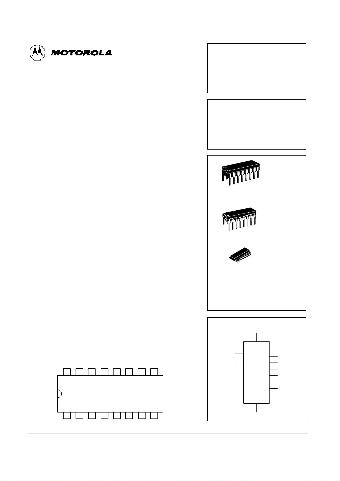
CONNECTION DIAGRAM
14 13 12 11 10 9
1 2 3 4 5 6
7
16 15
8
V
CC
S
1
B2A2S2A
3
S
3
B
3
C
4
B1A1S0A0B0C0GND
MC54/74F283
4-BIT BINARY FULL ADDER
(With Fast Carry)
FAST SCHOTTKY TTL
J SUFFIX
CERAMIC
CASE 620-09
N SUFFIX
PLASTIC
CASE 648-08
16
1
16
1
ORDERING INFORMATION
MC54FXXXJ Ceramic
MC74FXXXN Plastic
MC74FXXXD SOIC
16
1
D SUFFIX
SOIC
CASE 751B-03
LOGIC SYMBOL
VCC = PIN 16
GND = PIN 8
7
5
6
3
2
14
15
12
11
9
10
13
1
4 S
0
S
1
S
2
S
3
C
4
A
0
A
1
B
1
A
2
B
2
A
3
B
3
B
0
C
0
 Loading...