

4-143
FAST AND LS TTL DATA
9-BIT PARITY GENERATOR/
CHECKER
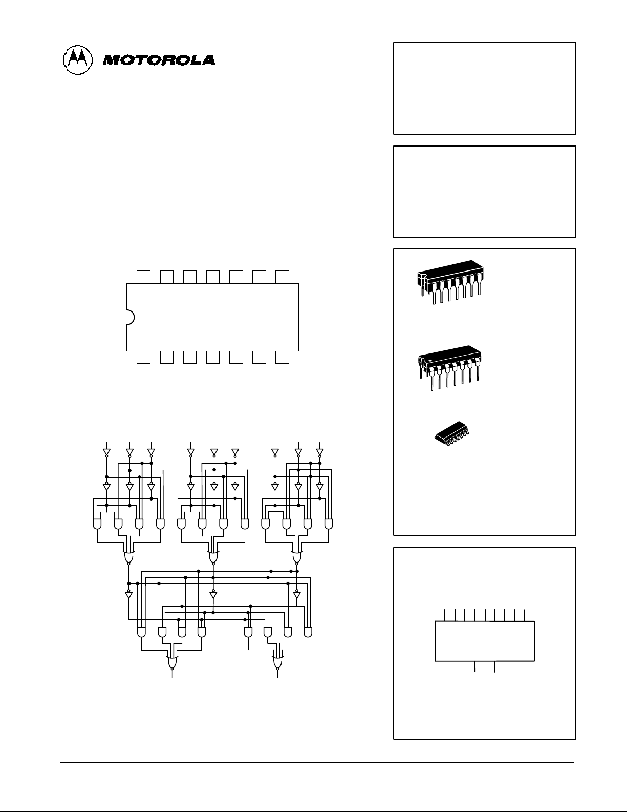
The MC54/74F280 is a high-speed parity generator/checker that accepts
nine bits of input data and detects whether an even or an odd number of these
inputs is HIGH. If an even number of inputs is HIGH, the Sum Even output is
HIGH. If an odd number is HIGH, the Sum Even output is LOW. The Sum Odd
output is the complement of the Sum Even output.
1314 12 11 10 9 8
21 3 4 5 6 7
GND
V
CC
CONNECTION DIAGRAM
I
5I4I3I2I1I0
I
6I7
NC I
8
∑E∑
O
NOTE:
This diagram is provided only for the understanding of logic operations and should not
be used to estimate propagation delays.
LOGIC DIAGRAM
I
0
I
1
I
2
I
3
I
4
I
5
I
6
I
7
I
8
Σ
E
Σ
O
14
1
D SUFFIX
SOIC
CASE 751A-02
N SUFFIX
PLASTIC
CASE 646-06
14
1
J SUFFIX
CERAMIC
CASE 632-08
14
1
MC54/74F280
9-BIT PARITY
GENERATOR/CHECKER
FAST SCHOTTKY TTL
ORDERING INFORMATION
MC54FXXXJ Ceramic
MC74FXXXN Plastic
MC74FXXXD SOIC
LOGIC SYMBOL
I0 I1 I
2
I
3
I4 I
5
I
6
I7 I
8
Σ
O
Σ
E
VCC = PIN 14
GND = PIN 7
8 9 10 11 1213 1 2 4
6 5
4-144
FAST AND LS TTL DATA
MC54/74F280
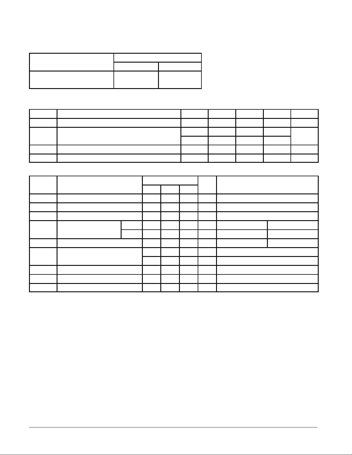
FUNCTION TABLE
Number of HIGH Inputs Outputs
I0-I
8
∑ Even ∑ Odd
0, 2, 4, 6, 8 H L
1, 3, 5, 7, 9 L H
H = HIGH Voltage Level; L = LOW Voltage Level
GUARANTEED OPERATING RANGES
Symbol Parameter Min Typ Max Unit
V
CC
Supply Voltage 54, 74 4.5 5.0 5.5 V
54 -55 25 125 °C
A
74 0 25 70
I
OH
Output Current — High 54, 74 –1.0 mA
I
OL
Output Current — Low 54, 74 20 mA
DC CHARACTERISTICS OVER OPERATING TEMPERATURE RANGE (unless otherwise specified)
Limits
Symbol Parameter Min Typ Max Unit Test Conditions
V
IH
Input HIGH Voltage 2.0 V Guaranteed Input HIGH Voltage for All Inputs
V
IL
Input LOW Voltage 0.8 V Guaranteed Input LOW Voltage for All Inputs
V
IK
Input Clamp Diode Voltage –1.2 V VCC = MIN, IIN = –18 MA
V
OH
Output HIGH Voltage 54, 74 2.5 3.4 V IOH = –1.0 mA VCC = 4.5 V
74 2.7 3.4 V IOH = 1.0 mA VCC = 4.75 V
V
OL
Output Low Voltage 0.35 0.5 V IOL = 20 mA VCC = MIN
I
IH
Input HIGH Current 20 µA VCC = MAX, VIN = 2.7 V
100 µA VCC = MAX, VIN = 7.0 V
I
IL
Input LOW Current –0.6 mA VCC = MAX, VIN = 0.5 V
I
OS
Short Circuit Current (Note 2) –60 –150 mA VCC = MAX, V
OUT
= 0 V
I
CC
Power Supply Current 25 38 mA VCC = MAX
NOTES:
1. For conditions shown as MIN or MAX, use the appropriate value specified under recommended operating conditions for the applicable device type.
2. Not more than one output should be shorted at a time, nor for more than 1 second.
T
A
Operating Ambient Temperature Range

4-145
FAST AND LS TTL DATA
MC54/74F280
AC CHARACTERISTICS
54/74F 54F 74F
TA = +25°C TA = –55°C to +125°C TA = 0°C to +70°C
VCC = +5.0 V VCC = 5.0 V ±10% VCC = 5.0 V ±10%
CL = 50 pF CL = 50 pF CL = 50 pF
Symbol Parameter Min Max Min Max Min Max Unit
t
PLH
Propagation Delay 4.5 15 4.5 20 4.5 16 ns
t
PHL
In to ∑
E
4.5 16 4.5 21 4.5 17
t
PLH
Propagation Delay 4.5 15 4.5 20 4.5 16 ns
t
PHL
In to ∑
O
4.5 16 4.5 21 4.5 17
 Loading...