

4-138
FAST AND LS TTL DATA
8-BIT BIDIRECTIONAL
BINARY COUNTER
The MC74F269 is a fully synchronous 8-stage up/down counter featuring
a preset capability for programmable operation, carry look-ahead for easy
cascading and a U/D
input to control the direction of counting. All state
changes, whether in counting or parallel loading, are initiated by the rising
edge of the clock.
• Synchronous Counting and Loading
• Built-In Lookahead Carry Capability
• Count Frequency 115 MHz Typical
• Supply Current 95 mA Typical
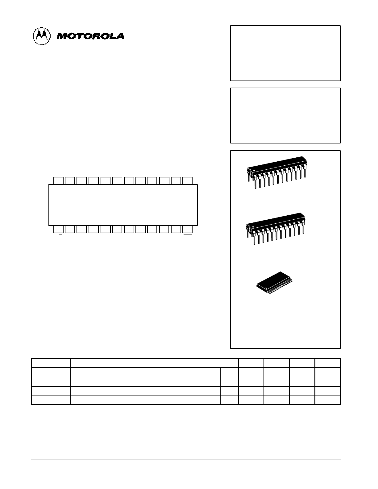
PIN ASSIGNMENT
22 21 20 19 18 17
1 2 3 4 5 6
7
24 23
8
PE
U/D
P0P1P2P
3
P
4
V
CC
P
5
Q0Q1Q2Q3Q4GND Q
5
9 10
11
12
Q6Q7CP CEP
16 15 14 13
P
6
TC
P
7
CET
GUARANTEED OPERATING RANGES
Symbol Parameter Min Typ Max Unit
V
CC
Supply Voltage 74 4.5 5.0 5.5 V
T
A
Operating Ambient Temperature Range 74 0 25 70 °C
I
OH
Output Current High 74 –1.0 mA
I
OL
Output Current Low 74 20 mA
MC74F269
8-BIT BIDIRECTIONAL
BINARY COUNTER
FAST SCHOTTKY TTL
ORDERING INFORMATION
MC74FXXXJ Ceramic
MC74FXXXN Plastic
MC74FXXXDW SOIC
N SUFFIX
PLASTIC
CASE 724-03
DW SUFFIX
SOIC
CASE 751E-03
24
1
24
1
J SUFFIX
CERAMIC
CASE 758-01
24
1
4-139
FAST AND LS TTL DATA
MC74F269
FUNCTION TABLE
Inputs Outputs
Operating Mode CP U/D CEP CET PE P
n
Q
n
TC
↑
Parallel Load
↑↑XXXXXXlll
h
L
H
(a)
(a)
Count Up ↑ h l l h X Count Up (a)
Count Down ↑ l l l h X Count Down (a)
↑
Hold
Do Nothing
↑↑XXhXXhhhX
X
q
n
q
n
(a)
H
H = HIGH voltage level steady state
h = HIGH voltage level one set-up time prior to the LOW-to-HIGH clock transition
L = LOW voltage level steady state
l = LOW voltage level one set-up time prior to the LOW-to-HIGH clock transition
X = Don’t care
q = Lower case letters indicate the state of the referenced output prior to the LOW-to-HIGH clock transition
↑ = LOW-to-HIGH clock transition
(a) = The TC
is LOW when CET is LOW and the counter is at Terminal Count. Terminal Count Up is with all Qn outputs HIGH and Terminal Count Down is with all
(a) = Qn outputs LOW.
DC CHARACTERISTICS OVER OPERATING TEMPERATURE RANGE (Unless otherwise specified)
Limits
Symbol
Parameter
Min Typ Max
Unit
Test Conditions
2.5
VCC = 4.5 V
VOHOutput HIGH Voltage
74
2.7 3.4
V
IOH = –1.0 mA
VCC = 4.75 V
V
OL
Output LOW Voltage 74 0.35 0.5 V IOL = 20 mA, VCC = 4.5 V
V
IK
Input Clamp Diode Voltage –1.2 V VCC = MIN, IIN = –18 mA
100
VIN = 7.0 V
IIHInput HIGH Current
20
µA
VCC = MAX
VIN = 2.7 V
I
IL
Input LOW Current –0.6 mA VCC = MAX, VIN = 0.5 V
I
OS
Output Short Circuit Current (Note 2) –60 –150 mA VCC = MAX, V
OUT
= 0 V
I
CCH
93 120
(Note 3)
ICCTotal Supply Current (total)
I
CCL
98 125
mA
VCC = MAX
(Note 4)
NOTES:
1. For conditions shown as MIN or MAX, use the appropriate value specified under guaranteed operating conditions for the applicable device type.
2. Not more than one output should be shorted at a time, nor for more than 1 second.
3. PE
= CET = CEP = U/D = GND: Pn = 4.5 V: CP = ↑
4. PE
= CET = CEP = U/D = GND: CP = ↑
X
X
X
l
l
Hold
X
h
X
h
X
L
q
(a)
(a)
 Loading...