

Motorola MC74ACT244DW, MC74ACT244N Datasheet
5-1
FACT DATA
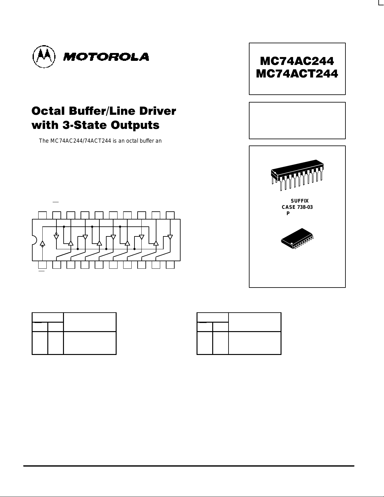
The MC74AC244/74ACT244 is an octal buffer and line driver designed to be
employed as a memory address driver, clock driver and bus oriented transmitter/
receiver which provides improved PC board density.
• 3-State Outputs Drive Bus Lines or Buffer Memory Address Registers
• Outputs Source/Sink 24 mA
• ′ACT244 Has TTL Compatible Inputs
1920 18 17 16 15 14
21 3 4 5 6 7
V
CC
13
8
12
9
11
10
OE
2
OE
1
GND
TRUTH TABLE
Inputs Outputs
OE1D (Pins 12, 14, 16, 18)
L L L
L H H
H X Z
H = HIGH Voltage Level
L = LOW Voltage Level
X = Immaterial
Z = High Impedance
TRUTH TABLE
Inputs Outputs
OE2D (Pins 3, 5, 7, 9)
L L L
L H H
H X Z
H = HIGH Voltage Level
L = LOW Voltage Level
X = Immaterial
Z = High Impedance
OCTAL BUFFER/LINE
DRIVER WITH
3-STATE OUTPUTS
N SUFFIX
CASE 738-03
PLASTIC
DW SUFFIX
CASE 751D-04
PLASTIC
MC74AC244 MC74ACT244
5-2
FACT DATA
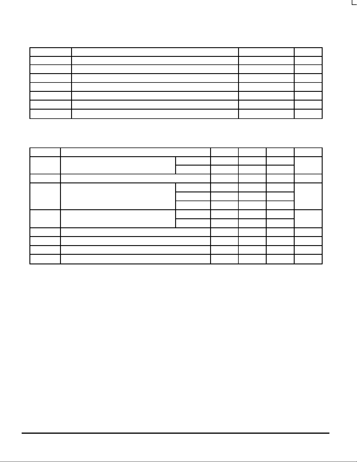
MAXIMUM RATINGS*
Symbol Parameter Value Unit
V
CC
DC Supply Voltage (Referenced to GND) –0.5 to +7.0 V
V
in
DC Input Voltage (Referenced to GND) –0.5 to VCC +0.5 V
V
out
DC Output Voltage (Referenced to GND) –0.5 to VCC +0.5 V
I
in
DC Input Current, per Pin ±20 mA
I
out
DC Output Sink/Source Current, per Pin ±50 mA
I
CC
DC VCC or GND Current per Output Pin ±50 mA
T
stg
Storage Temperature –65 to +150 °C
* Maximum Ratings are those values beyond which damage to the device may occur. Functional operation should be restricted to the Recommended
Operating Conditions.
RECOMMENDED OPERATING CONDITIONS
Symbol Parameter Min Typ Max Unit
′AC 2.0 5.0 6.0
VCCSupply Voltage
′ACT 4.5 5.0 5.5
V
Vin, V
out
DC Input Voltage, Output Voltage (Ref. to GND) 0 V
CC
V
VCC @ 3.0 V 150
Input Rise and Fall Time (Note 1)
′AC Devices except Schmitt Inputs
VCC @ 4.5 V 40 ns/V
r
, t
f
′AC Devices except Schmitt Inputs
VCC @ 5.5 V 25
VCC @ 4.5 V 10
tr, t
f
Input Rise and Fall Time (Note 2)
′ACT Devices except Schmitt Inputs
VCC @ 5.5 V 8.0
ns/V
T
J
Junction Temperature (PDIP) 140 °C
T
A
Operating Ambient Temperature Range –40 25 85 °C
I
OH
Output Current — High –24 mA
I
OL
Output Current — Low 24 mA
1. Vin from 30% to 70% VCC; see individual Data Sheets for devices that differ from the typical input rise and fall times.
2. Vin from 0.8 V to 2.0 V; see individual Data Sheets for devices that differ from the typical input rise and fall times.
tr, t
f
Input Rise and Fall Time (Note 2)
 Loading...