

Motorola MC74ACT132D, MC74ACT132J, MC74AC132J, MC74AC132D, MC74AC132N Datasheet
5-1
FACT DATA
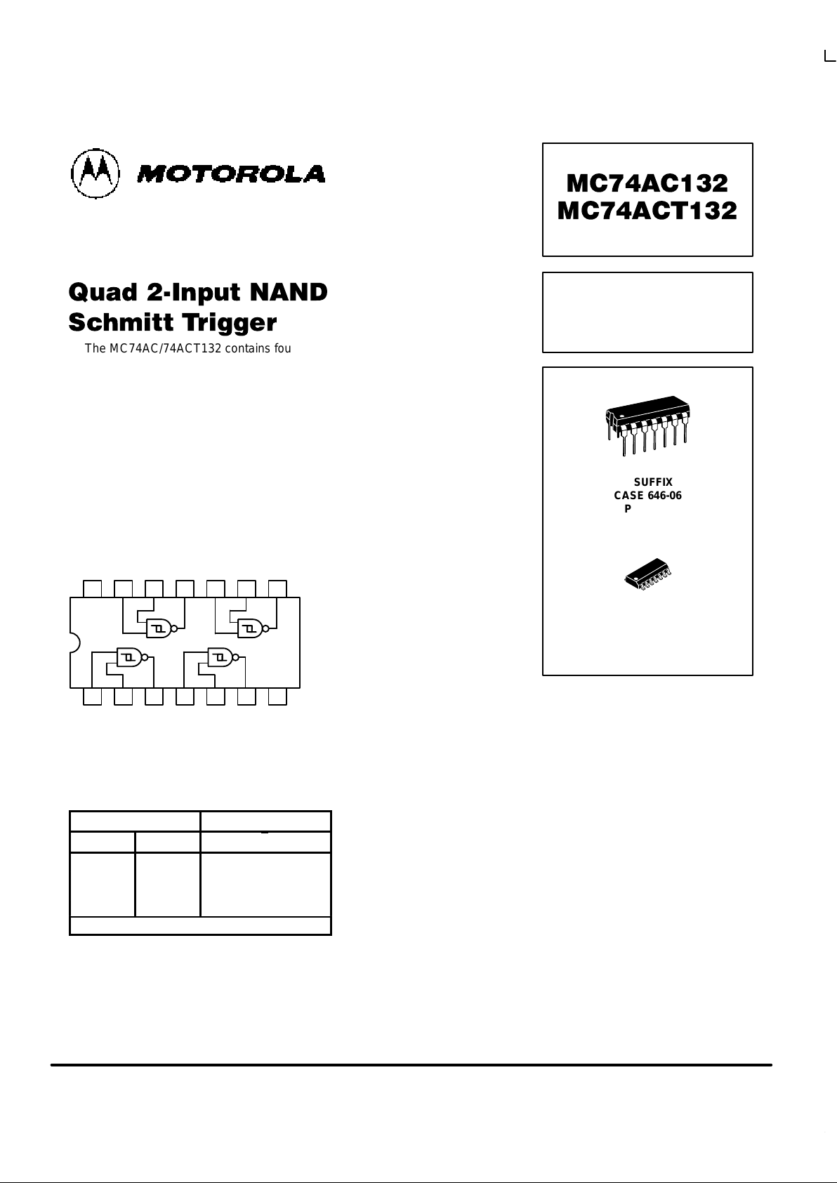
The MC74AC/74ACT132 contains four 2-input NAND gates which are capable
of transforming slowly changing input signals into sharply defined, jitter-free output
signals. In addition, they have greater noise margin than conventional NAND gates.
Each circuit contains a 2-input Schmitt trigger. The Schmitt trigger uses positive
feedback to effectively speed-up slow input transitions, and provide different input
threshold voltages for positive and negative-going transitions. This hysteresis
between the positive-going and negative-going input threshold is determined by
resistor ratios and is essentially insensitive to temperature and supply voltage
variations.
• Schmitt Trigger Inputs
• Outputs Source/Sink 24 mA
• ′ACT132 Has TTL Compatible Inputs
1314 12 11 10 9 8
21 3 4 5 6 7
GND
V
CC
J Suffix — Case 632-08 (Ceramic)
N Suffix — Case 646-06 (Plastic)
D Suffix — Case 751A-03 (SOIC)
PIN CONFIGURATION
FUNCTION TABLE
Inputs Output
A B Y
L L H
L H H
H L H
H H L
H = HIGH Voltage Level L = LOW Voltage Level
QUAD 2-INPUT
NAND
SCHMITT TRIGGER
N SUFFIX
CASE 646-06
PLASTIC
D SUFFIX
CASE 751A-03
PLASTIC
MC74AC132 MC74ACT132
5-2
FACT DATA
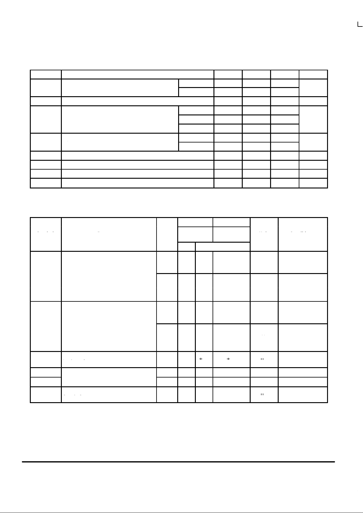
RECOMMENDED OPERATING CONDITIONS
Symbol Parameter Min Typ Max Unit
′AC 2.0 5.0 6.0
VCCSupply Voltage
′ACT 4.5 5.0 5.5
V
Vin, V
out
DC Input Voltage, Output Voltage (Ref. to GND) 0 V
CC
V
VCC @ 3.0 V 150
tr, t
f
Input Rise and Fall Time (Note 1)
′AC Devices except Schmitt Inputs
VCC @ 4.5 V 40 ns/V
r
, t
f
′AC Devices except Schmitt Inputs
VCC @ 5.5 V 25
Input Rise and Fall Time (Note 2)
VCC @ 4.5 V 10
tr, t
f
Input Rise and Fall Time (Note 2)
′ACT Devices except Schmitt Inputs
VCC @ 5.5 V 8.0
ns/V
T
J
Junction Temperature (PDIP) 140 °C
T
A
Operating Ambient Temperature Range –40 25 85 °C
I
OH
Output Current — High –24 mA
I
OL
Output Current — Low 24 mA
1. Vin from 30% to 70% VCC; see individual Data Sheets for devices that differ from the typical input rise and fall times.
2. Vin from 0.8 V to 2.0 V; see individual Data Sheets for devices that differ from the typical input rise and fall times.
DC CHARACTERISTICS
74AC 74AC
Symbol
Parameter
V
CC
(V)
TA = +25°C
TA =
–40°C to +85°C
Unit
Conditions
Typ Guaranteed Limits
V
OH
Minimum High Level
3.0 2.99 2.9 2.9 I
OUT
= –50 µA
Output Voltage
4.5 4.49 4.4 4.4 V
5.5 5.49 5.4 5.4
*VIN = VIL or V
IH
3.0 2.56 2.46
–12 mA
4.5 3.86 3.76
V
I
OH
–24 mA
5.5 4.86 4.76 –24 mA
V
OL
Maximum Low Level
3.0 0.002 0.1 0.1 I
OUT
= 50 µA
Output Voltage
4.5 0.001 0.1 0.1 V
5.5 0.001 0.1 0.1
*VIN = VIL or V
IH
3.0 0.36 0.44
12 mA
4.5 0.36 0.44
V
I
OL
24 mA
5.5 0.36 0.44 24 mA
I
IN
Maximum Input
Leakage Current
5.5
±0.1
±1.0
µA
VI = VCC, GND
I
OLD
†Minimum Dynamic
5.5 75 mA V
OLD
= 1.65 V Max
I
OHD
Output Current
5.5 –75 mA V
OHD
= 3.85 V Min
I
CC
Maximum Quiescent
Supply Current
5.5
4.040µA
VIN = VCC or GND
* All outputs loaded; thresholds on input associated with output under test.
†Maximum test duration 2.0 ms, one output loaded at a time.
Note: IIN and ICC @ 3.0 V are guaranteed to be less than or equal to the respective limit @ 5.5 V VCC.
 Loading...