

Motorola MC74ACT113N, MC74ACT113D, MC74AC113N, MC74AC113D Datasheet
5-1
FACT DATA
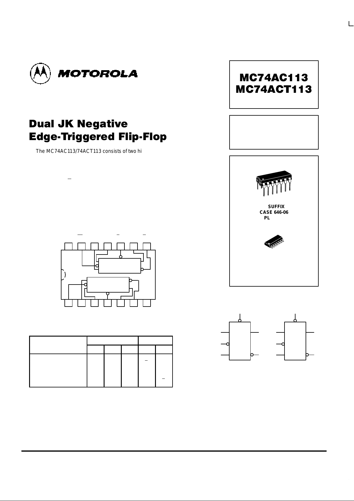
The MC74AC113/74ACT113 consists of two high-speed completely independent
transition clocked JK flip-flops. The clocking operation is independent of rise and fall
times of the clock waveform. The JK design allows operation as a D flip-flop (refer to
MC74AC74/74ACT74 data sheet) by connecting the J and K inputs together.
Asynchronous Inputs:
LOW input to S
D
(Set) sets Q to HIGH level
Set is independent of clock
• Outputs Source/Sink 24 mA
• ′ACT113 Has TTL Compatible Inputs
1112
V
CC
CP
1K1J1SD1Q1Q1
CP
2K2J2SD2Q2Q2
CP
Q
GND
S
D
CONNECTION DIAGRAM
1 2 3 4 5 6 7
89101314
Q
CP
Q
S
D
Q
K
J
J
K
MODE SELECT — TRUTH TABLE
Inputs Outputs
Operating Mode
S
D
J K Q Q
Set L X X H L
Toggle H h h q q
Load “0” (Reset) H l h L H
Load “1” (Set) H h l H L
Hold H l l q q
H, h = HIGH Voltage Level
L, l = LOW Voltage Level
X = Don’t Care
l, h (q) = Lower case letters indicate the state of the referenced input
(or output) one set-up time prior to the HIGH to LOW clock transition.
DUAL JK NEGATIVE
EDGE-TRIGGERED
FLIP-FLOP
N SUFFIX
CASE 646-06
PLASTIC
D SUFFIX
CASE 751A-03
PLASTIC
LOGIC SYMBOL
S
D
QJ
CP
Q
VCC = PIN 14
GND = PIN 7
K
3
1
2
4
5
6
S
D
QJ
CP
Q
K
11
13
12
10
9
8
MC74AC113 MC74ACT113
5-2
FACT DATA
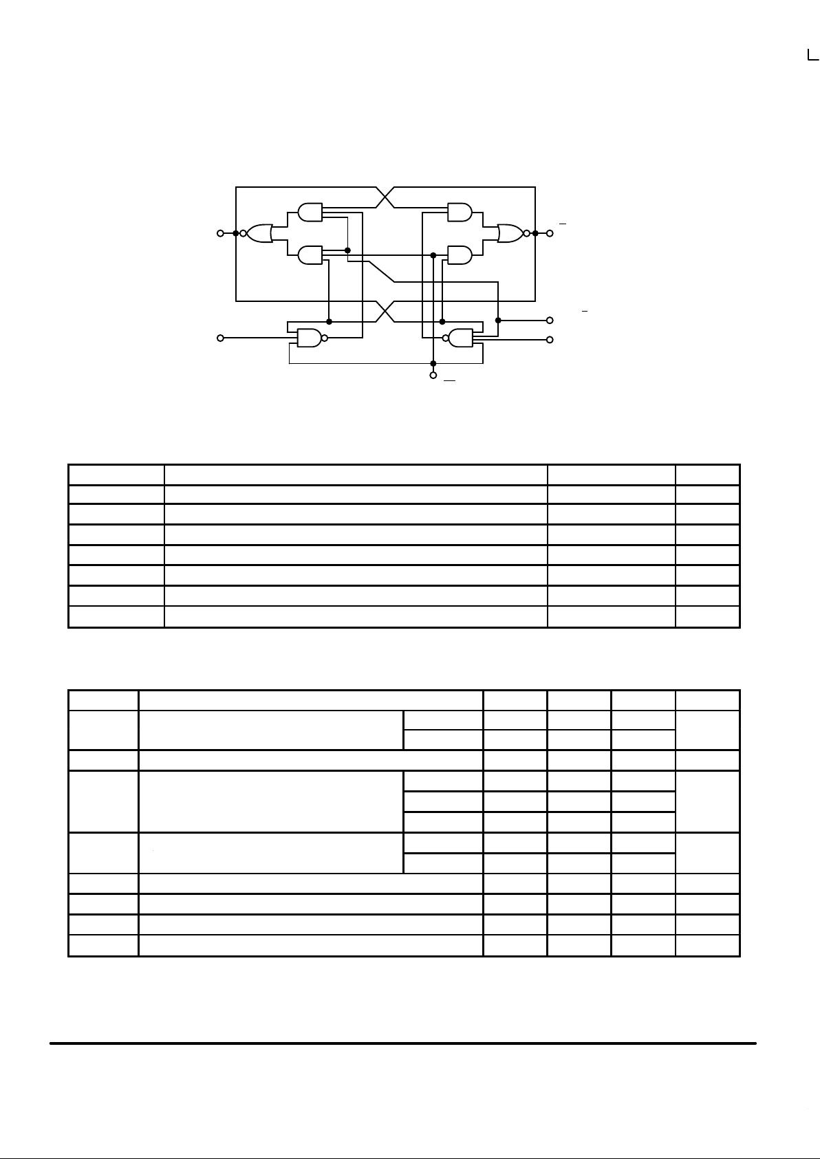
Q
LOGIC DIAGRAM (Each Flip-Flop)
J
Q
SET (S
D
)
K
6(8)
4(10)
2(12)
CLOCK (CP
)
1(13)
3(11)
5(9)
MAXIMUM RATINGS*
Symbol Parameter Value Unit
V
CC
DC Supply Voltage (Referenced to GND) –0.5 to +7.0 V
V
in
DC Input Voltage (Referenced to GND) –0.5 to VCC +0.5 V
V
out
DC Output Voltage (Referenced to GND) –0.5 to VCC +0.5 V
I
in
DC Input Current, per Pin ±20 mA
I
out
DC Output Sink/Source Current, per Pin ±50 mA
I
CC
DC VCC or GND Current per Output Pin ±50 mA
T
stg
Storage Temperature –65 to +150 °C
* Maximum Ratings are those values beyond which damage to the device may occur. Functional operation should be restricted to the Recommended
Operating Conditions.
RECOMMENDED OPERATING CONDITIONS
Symbol Parameter Min Typ Max Unit
′AC 2.0 5.0 6.0
VCCSupply Voltage
′ACT 4.5 5.0 5.5
V
Vin, V
out
DC Input Voltage, Output Voltage (Ref. to GND) 0 V
CC
V
VCC @ 3.0 V 150
tr, t
f
Input Rise and Fall Time (Note 1)
′AC Devices except Schmitt Inputs
VCC @ 4.5 V 40 ns/V
r
, t
f
′AC Devices except Schmitt Inputs
VCC @ 5.5 V 25
Input Rise and Fall Time (Note 2)
VCC @ 4.5 V 10
tr, t
f
Input Rise and Fall Time (Note 2)
′ACT Devices except Schmitt Inputs
VCC @ 5.5 V 8.0
ns/V
T
J
Junction Temperature (PDIP) 140 °C
T
A
Operating Ambient Temperature Range –40 25 85 °C
I
OH
Output Current — High –24 mA
I
OL
Output Current — Low 24 mA
1. Vin from 30% to 70% VCC; see individual Data Sheets for devices that differ from the typical input rise and fall times.
2. Vin from 0.8 V to 2.0 V; see individual Data Sheets for devices that differ from the typical input rise and fall times.
 Loading...