

Motorola MC74AC4020N, MC74AC4020D Datasheet
5-1
FACT DATA
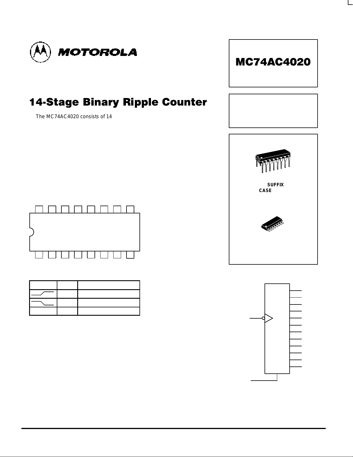
The MC74AC4020 consists of 14 master-slave flip-flops with 12 stages
brought out to pins. The output of each flip-flop feeds the next and the frequency
at each output is half that of the preceding one. The state of the counter
advances on the negative-going edge of the Clock input. Reset is asynchronous
and active-high.
State changes of the Q outputs do not occur simultaneously because of internal
ripple delays. Therefore, decoded output signals are subject to decoding spikes
and may have to be gated with the Clock of the MC74AC4020 for some designs.
• 140 MHz Typ. Clock
• Outputs Source/Sink 24 mA
• Operating Voltage Range: 2.0 to 6.0 V
• High Noise Immunity
1516 14 13 12 11 10
21 3 4 5 6 7
V
CC
9
8
Q11 Q10 Q8 Q9 RESET CLK Q1
Q12 Q13 Q14 Q6 Q5 Q7 Q4 GND
FUNCTION TABLE
Clock Reset Output State
L No Change
L Advance to next state
X H All Outputs are low
14-STAGE
BINARY RIPPLE
COUNTER
N SUFFIX
CASE 648-08
PLASTIC
D SUFFIX
CASE 751B-05
PLASTIC
LOGIC DIAGRAM
CLOCK
10
11
RESET
PIN 16 = V
CC
PIN 8 = GND
9
7
5
4
6
13
12
14
15
1
2
3
Q1
Q4
Q5
Q6
Q7
Q8
Q9
Q10
Q11
Q12
Q13
Q14
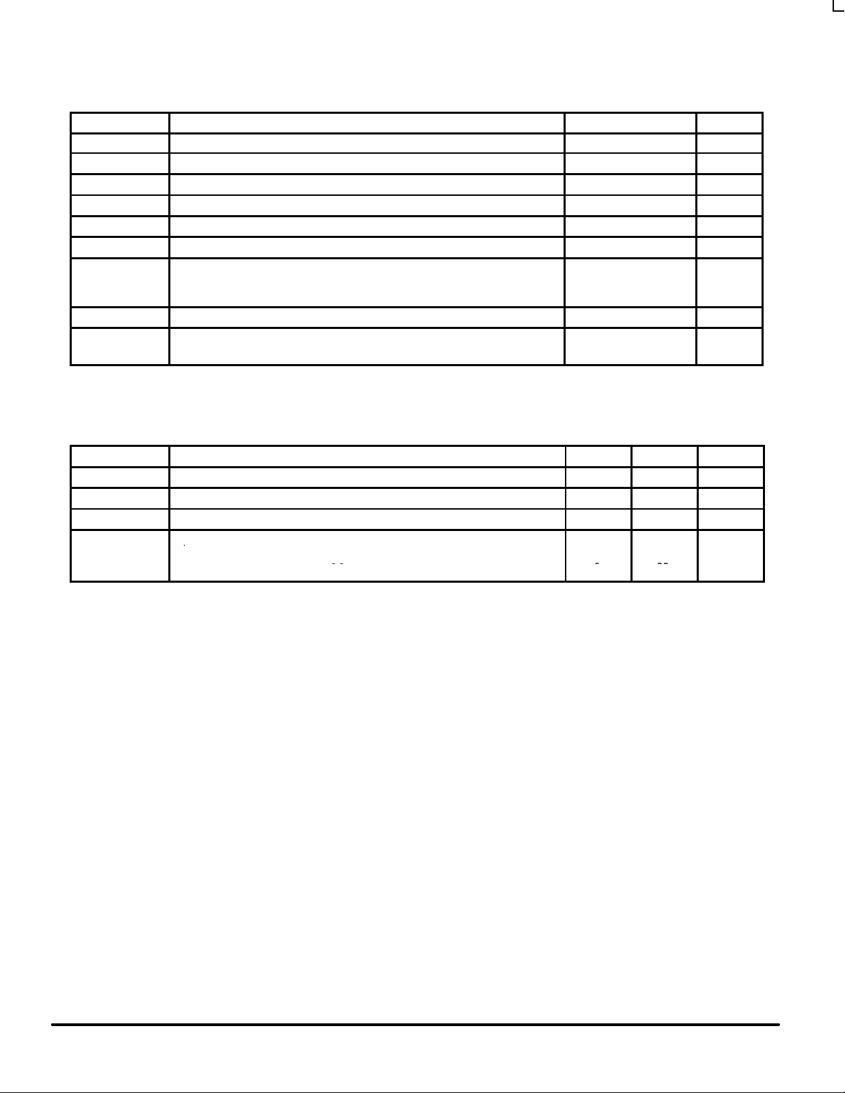
MC74AC4020
5-2
FACT DATA
MAXIMUM RATINGS*
Symbol Parameter Value Unit
V
CC
DC Supply Voltage (Referenced to GND) –0.5 to +7.0 V
V
in
DC Input Voltage (Referenced to GND) –0.5 to VCC +0.5 V
V
out
DC Output Voltage (Referenced to GND) –0.5 to VCC +0.5 V
I
in
DC Input Current, per Pin ±20 mA
I
out
DC Output Current, per Pin ±50 mA
I
CC
DC VCC or GND Current per Output Pin ±50 mA
P
D
Power Dissipation in Still Air
Plastic**
SOIC Package**
750
500
mW
T
stg
Storage Temperature –65 to +150 °C
T
L
Lead Temperature, 1 mm from Case for 10 seconds
(Plastic DIP or SOIC Package)
260 °C
* Maximum Ratings are those values beyond which damage to the device may occur.
** Derating: Plastic DIP: – 10mW/°C from 65°C to 125°C
SOIC Package: –7.0 mW/°C from 65°C to 125°C
RECOMMENDED OPERATING CONDITIONS
Symbol Parameter Min Max Unit
V
CC
DC Supply Voltage (Referenced to GND) 2.0 6.0 V
Vin/V
out
Input Voltage, Output Voltage (Ref. to GND) 0 V
CC
T
A
Operating Temperature, All Package Types –40 +85 °C
/t
= 3.0 V
tr/tfInput Rise/Fall Time
(Figure 1)
VCC = 3.0 V
VCC = 4.5 V
0015040ns/V
VCC = 5.5 V
t
Input Rise/Fall Time V
0 150 ns/V
0 25
 Loading...