

MOTOROLA MC74AC259, MC74ACT259 Technical data
5-1
FACT DATA
The MC74AC259/74ACT259 is a high-speed 8-bit addressable latch designed for
general purpose storage applications in digital systems. It is a multifunctional device
capable of storing single line data in eight addressable latches, and also a 1-of-8
decoder and demultiplexer with active HIGH outputs. The device also incorporates
an active LOW Common Clear for resetting all latches, as well as an active LOW
Enable. It is functionally identical to the ALS259 8-bit addressable latch.
• Serial-to-Parallel Conversion
• Eight Bits of Storage with Output of Each Bit Available
• Random (Addressable) Data Entry
• Active High Demultiplexing or Decoding Capability
• Easily Expandable
• Common Clear
FUNCTIONAL DESCRIPTION
The MC74AC259/74ACT259 has four modes of operation as shown in the Mode
Selection Table. In the addressable latch mode, data on the Data line (D) is written
into the addressed latch. The addressed latch will follow the data input with all nonaddressed latches remaining in their previous states in the memory mode. All latches
remain in their previous state and are unaffected by the Data or Address inputs.
In the one-of-eight decoding or demultiplexing mode, the addressed output will
follow the state of the D input with all other outputs in the LOW state. In the clear
mode all outputs are LOW and unaffected by the address and data inputs. When
operating the MC74AC/ACT259 as an addressable latch, changing more than one
bit of the address could impose a transient wrong address. Therefore, this should
only be done while in the memory mode. The Mode Select Function Table
summarizes the operations of the MC74AC/ACT259.
8-BIT
ADDRESSABLE
LATCH
N SUFFIX
CASE 648-08
PLASTIC
D SUFFIX
CASE 751B-05
PLASTIC
LOGIC SYMBOL
A
0
A
1
A
2
E D
MR Q0Q1Q2Q3Q4Q5Q6Q
7
1516 14 13 12 11 10
21 3 4 5 6 7
V
CC
9
8
MR E D Q7Q6Q5Q
4
A0A1A2Q0Q1Q2Q3GND
查询MC74AC259供应商
MC74AC259 MC74ACT259
5-2
FACT DATA
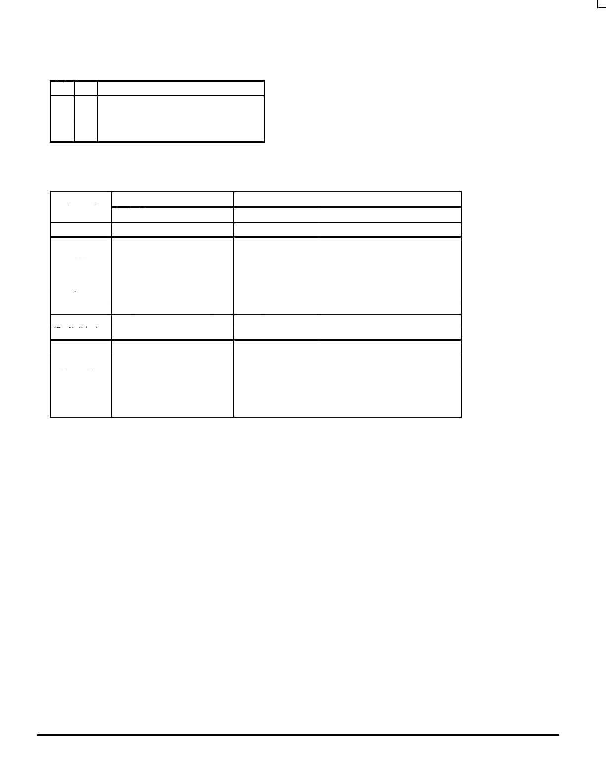
MODE SELECT TABLE
E MR Mode
L H Addressable Latch
H H Memory
L L Active HIGH 8-Channel Demultiplexer
H L Clear
H = HIGH Voltage Level
L = LOW Voltage Level
MODE SELECT-FUNCTION TABLE
Operating
Inputs Outputs
Operating
Mode
MR E D A0A1A2Q
0
Q
1
Q
2
Q
3
Q
4
Q
5
Q
6
Q
7
Master Reset L H X X X X L L L L L L L L
L L d L L L Q = d L L L L L L L
L L d H L L L Q = d L L L L L L
Demultiplex
L L d L H L L L Q = d L L L L L
(Active HIGH
• • • • • • • • • • • • • •
Decoder when
D = H)
• • • • • • • • • • • • • •
D = H)
• • • • • • • • • • • • • •
L L d H H H L L L L L L L Q = d
HHXXXXq0q1q2q3q4q5q6q
7
H L d L L L Q = d q
1
q
2
q
3
q
4
q
5
q
6
q
7
H L d H L L q0Q = d q
2
q
3
q
4
q
5
q
6
q
7
H L d L H L q
0
q1Q = d q
3
q
4
q
5
q
6
q
7
Addressable
• • • • • • • • • • • • • •
Latch
• • • • • • • • • • • • • •
• • • • • • • • • • • • • •
H L d H H H q
0
q
1
q
2
q
3
q
4
q
5
q6Q = d
H = HIGH Voltage Level
L = LOW Voltage Level
X = Immaterial
d = HIGH or LOW Data one setup time prior to the LOW-to-HIGH Enable transition
q = Lower case letters indicate the state of the referenced output established during the last cycle in which it was addressed
or cleared.
Store
(Do Nothing)
MC74AC259 MC74ACT259
5-3
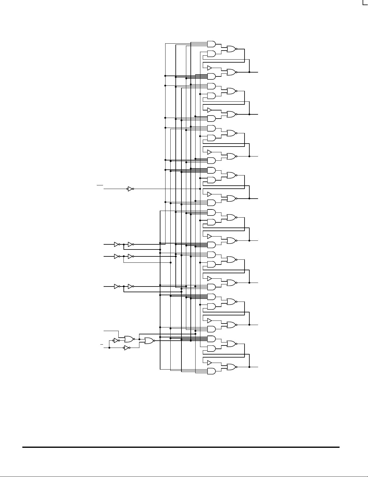
FACT DATA
MR
A
2
A
1
A
0
D
E
Q
7
Q
6
Q
5
Q
4
Q
3
Q
2
Q
1
Q
0
Please note that this diagram is provided only for the understanding of logic
operations and should not be used to estimate propagation delays.
 Loading...