

MOTOROLA MC74AC251, MC74ACT251 Technical data
5-1
FACT DATA
The MC74AC251/74ACT251 is a high-speed 8-input digital multiplexer. It
provides, in one package, the ability to select one bit of data from up to eight
sources. It can be used as a universal function generator to generate any logic
function of four variables. Both true and complementary outputs are provided.
• Multifunctional Capability
• On-Chip Select Logic Decoding
• Inverting and Noninverting 3-State Outputs
• Outputs Source/Sink 24 mA
• ′ACT251 Has TTL Compatible Inputs
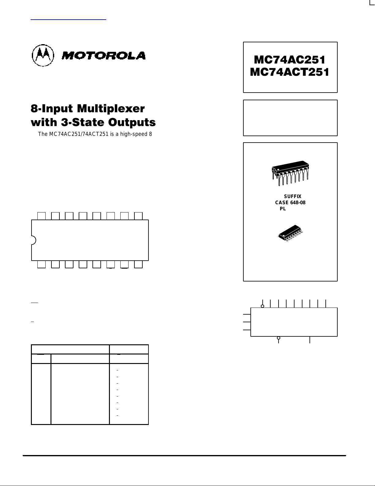
1516 14 13 12 11 10
21 3 4 5 6 7
V
CC
9
8
I
4I5I6I7S0S1S2
I
3I2I1I0
Z Z
OE GND
PIN NAMES
S0–S2Select Inputs
OE
3-State Output Enable Input
I0–I
7
Multiplexer Inputs
Z 3-State Multiplexer Output
Z
Complementary 3-State Multiplexer Output
TRUTH TABLE
Inputs Outputs
OE S
2
S
1
S
0
Z Z
H X X X Z Z
L L L L I
0
I
0
L L L H I
1
I
1
L L H L I
2
I
2
L L H H I
3
I
3
L H L L I
4
I
4
L H L H I
5
I
5
L H H L I
6
I
6
L H H H I
7
I
7
H = HIGH Voltage Level
L = LOW Voltage Level
X = Immaterial
Z = High Impedance
8-INPUT
MULTIPLEXER WITH
3-STATE OUTPUTS
N SUFFIX
CASE 648-08
PLASTIC
D SUFFIX
CASE 751B-05
PLASTIC
LOGIC SYMBOL
S
0
S
1
S
2
OE I0I1I2I3I4I5I6I
7
Z Z
查询MC74AC251供应商
MC74AC251 MC74ACT251
5-2
FACT DATA
FUNCTIONAL DESCRIPTION
This device is a logical implementation of a single-pole,
8-position switch with the switch position controlled by the
state of three Select inputs, S0, S1, S2. Both true and
complementary outputs are provided. The Output Enable
input (OE
) is active LOW. When it is activated, the logic
function provided at the output is:
Z = OE
•(I0•S0•S1•S
2+I1
•S0•S1•S
2
+
I
2
•S0•S1•S
2+I3
•S0•S1•S
2
+
I
4
•S0•S1•S
2+I5•S0
•S1•S
2
+
I
6
•S0•S1•S
2+I7•S0•S1•S2
)
When the Output Enable is HIGH, both outputs are in the
high impedance (High Z) state. This feature allows multiplexer
expansion by tying the outputs of up to 128 devices together .
When the outputs of the 3-state devices are tied together, all
but one device must be in the high impedance state to avoid
high currents that would exceed the maximum ratings. The
Output Enable signals should be designed to ensure there is
no overlap in the active-LOW portion of the enable voltages.
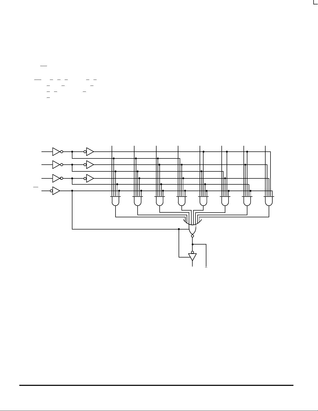
Please note that this diagram is provided
only for the understanding of logic
operations and should not be used to
estimate propagation delays.
LOGIC DIAGRAM
I
0
I
1
I
2
I
3
I
4
I
5
I
6
Z Z
S
2
S
1
S
0
OE
I
7
MC74AC251 MC74ACT251
5-3
FACT DATA
MAXIMUM RATINGS*
Symbol Parameter Value Unit
V
CC
DC Supply Voltage (Referenced to GND) –0.5 to +7.0 V
V
in
DC Input Voltage (Referenced to GND) –0.5 to VCC +0.5 V
V
out
DC Output Voltage (Referenced to GND) –0.5 to VCC +0.5 V
I
in
DC Input Current, per Pin ±20 mA
I
out
DC Output Sink/Source Current, per Pin ±50 mA
I
CC
DC VCC or GND Current per Output Pin ±50 mA
T
stg
Storage Temperature –65 to +150 °C
* Maximum Ratings are those values beyond which damage to the device may occur. Functional operation should be restricted to the Recommended
Operating Conditions.
RECOMMENDED OPERATING CONDITIONS
Symbol Parameter Min Typ Max Unit
′AC 2.0 5.0 6.0
VCCSupply Voltage
′ACT 4.5 5.0 5.5
V
Vin, V
out
DC Input Voltage, Output Voltage (Ref. to GND) 0 V
CC
V
VCC @ 3.0 V 150
Input Rise and Fall Time (Note 1)
′AC Devices except Schmitt Inputs
VCC @ 4.5 V 40 ns/V
r
, t
f
′AC Devices except Schmitt Inputs
VCC @ 5.5 V 25
VCC @ 4.5 V 10
tr, t
f
Input Rise and Fall Time (Note 2)
′ACT Devices except Schmitt Inputs
VCC @ 5.5 V 8.0
ns/V
T
J
Junction Temperature (PDIP) 140 °C
T
A
Operating Ambient Temperature Range –40 25 85 °C
I
OH
Output Current — High –24 mA
I
OL
Output Current — Low 24 mA
1. Vin from 30% to 70% VCC; see individual Data Sheets for devices that differ from the typical input rise and fall times.
2. Vin from 0.8 V to 2.0 V; see individual Data Sheets for devices that differ from the typical input rise and fall times.
tr, t
f
Input Rise and Fall Time (Note 2)
 Loading...