

MOTOROLA MC74ACT245ML1, MC74ACT245ML2, MC74ACT245MR1, MC74ACT245MR2, MC74ACT245DTR2 Datasheet
...
5-1
FACT DATA
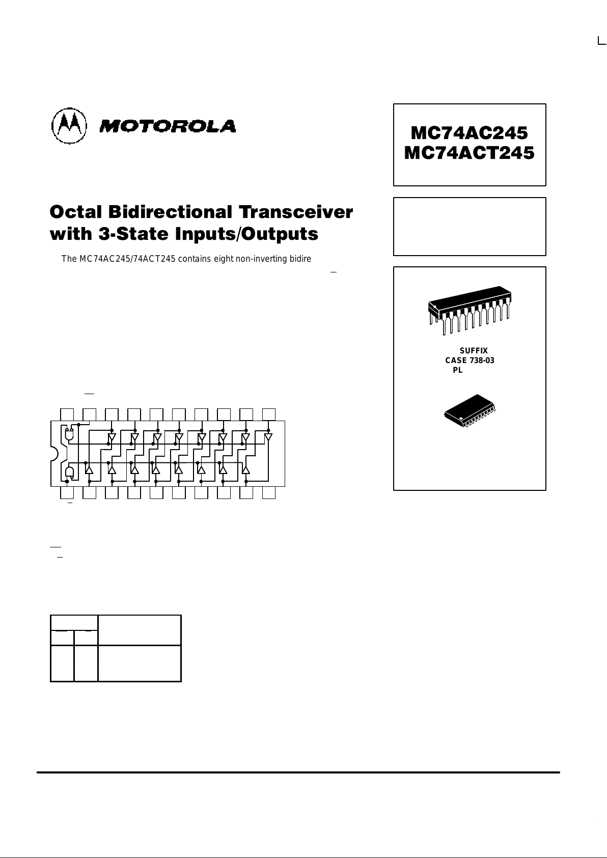
The MC74AC245/74ACT245 contains eight non-inverting bidirectional buffers
with 3-state outputs and is intended for bus-oriented applications. Current sinking
capability is 24 mA at both the A and B ports. The Transmit/Receive (T/R
) input
determines the direction of data flow through the bidirectional transceiver. Transmit
(active-HIGH) enables data from A ports to B ports; Receive (active-LOW) enables
data from B ports to A ports. The Output Enable input, when HIGH, disables both A
and B ports by placing them in a High Z condition.
• Noninverting Buffers
• Bidirectional Data Path
• A and B Outputs Source/Sink 24 mA
• ′ACT245 Has TTL Compatible Inputs
1920 18 17 16 15 14
21 3 4 5 6 7
V
CC
13
8
12
9
11
10
OE
B0B1B2B3B4B5B6B
7
T/R
A0A1A2A3A4A5A6A7GND
PIN NAMES
OE
Output Enable Input
T/R
Transmit/Receive Input
A0–A7Side A 3-State Inputs or 3-State Outputs
B0–B7Side B 3-State Inputs or 3-State Outputs
TRUTH TABLES
Inputs
OE T/R
Outputs
L L Bus B Data to Bus A
L H Bus A Data to Bus B
H X High Z State
H = HIGH Voltage Level
L = LOW Voltage Level
X = Immaterial
OCTAL BIDIRECTIONAL
TRANSCEIVER
WITH 3-STATE
INPUTS/OUTPUTS
N SUFFIX
CASE 738-03
PLASTIC
DW SUFFIX
CASE 751D-04
PLASTIC
MC74AC245 MC74ACT245
5-2
FACT DATA
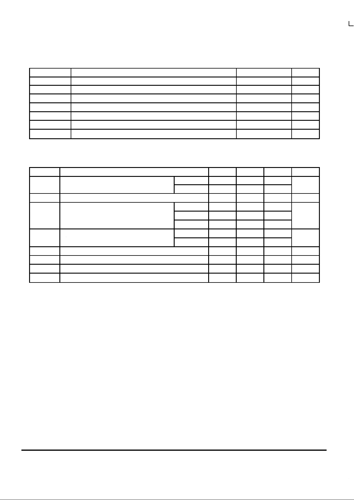
MAXIMUM RATINGS*
Symbol Parameter Value Unit
V
CC
DC Supply Voltage (Referenced to GND) –0.5 to +7.0 V
V
in
DC Input Voltage (Referenced to GND) –0.5 to VCC +0.5 V
V
out
DC Output Voltage (Referenced to GND) –0.5 to VCC +0.5 V
I
in
DC Input Current, per Pin ±20 mA
I
out
DC Output Sink/Source Current, per Pin ±50 mA
I
CC
DC VCC or GND Current per Output Pin ±50 mA
T
stg
Storage Temperature –65 to +150 °C
* Maximum Ratings are those values beyond which damage to the device may occur. Functional operation should be restricted to the Recommended
Operating Conditions.
RECOMMENDED OPERATING CONDITIONS
Symbol Parameter Min Typ Max Unit
′AC 2.0 5.0 6.0
VCCSupply Voltage
′ACT 4.5 5.0 5.5
V
Vin, V
out
DC Input Voltage, Output Voltage (Ref. to GND) 0 V
CC
V
VCC @ 3.0 V 150
tr, t
f
Input Rise and Fall Time (Note 1)
′AC Devices except Schmitt Inputs
VCC @ 4.5 V 40 ns/V
r
, t
f
′AC Devices except Schmitt Inputs
VCC @ 5.5 V 25
Input Rise and Fall Time (Note 2)
VCC @ 4.5 V 10
tr, t
f
Input Rise and Fall Time (Note 2)
′ACT Devices except Schmitt Inputs
VCC @ 5.5 V 8.0
ns/V
T
J
Junction Temperature (PDIP) 140 °C
T
A
Operating Ambient Temperature Range –40 25 85 °C
I
OH
Output Current — High –24 mA
I
OL
Output Current — Low 24 mA
1. Vin from 30% to 70% VCC; see individual Data Sheets for devices that differ from the typical input rise and fall times.
2. Vin from 0.8 V to 2.0 V; see individual Data Sheets for devices that differ from the typical input rise and fall times.
 Loading...