

MOTOROLA MC74ACT20MEL, MC74ACT20ML1, MC74ACT20ML2, MC74ACT20MR1, MC74ACT20MR2 Datasheet
...
5-1
FACT DATA
• Outputs Source/Sink 24 mA
• ′ACT20 Has TTL Compatible Inputs
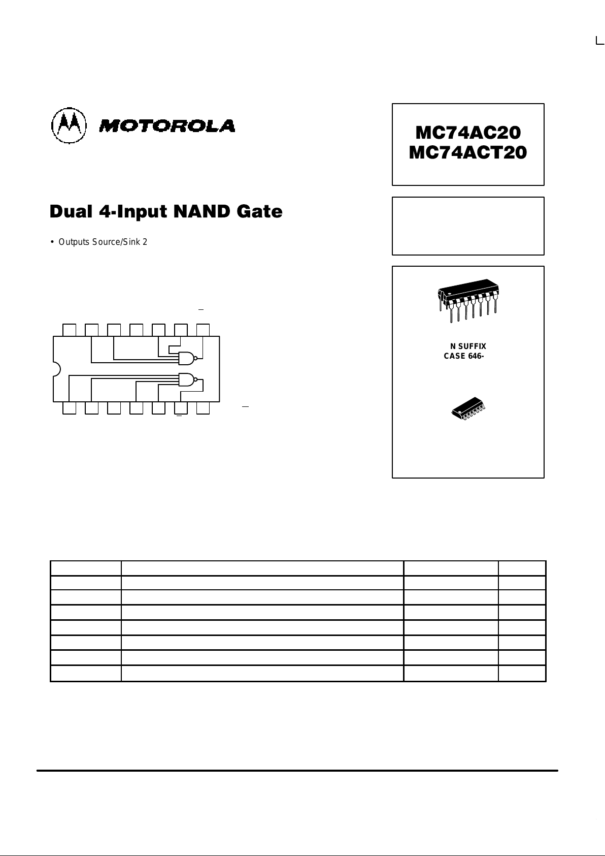
Pinout: 14-Lead Packages (Top View)
GND
1314 12 11 10 9 8
21 3 4 5 6 7
VCCA1B1NC C1D1O
1
A0B0NC C0D0O
0
PIN NAMES
An, Bn, Cn, D
n
Inputs
O
n
Outputs
MAXIMUM RATINGS*
Symbol Parameter Value Unit
V
CC
DC Supply Voltage (Referenced to GND) –0.5 to +7.0 V
V
in
DC Input Voltage (Referenced to GND) –0.5 to VCC + 0.5 V
V
out
DC Output Voltage (Referenced to GND) –0.5 to VCC + 0.5 V
I
in
DC Input Current, per Pin ± 20 mA
I
out
DC Output Sink/Source Current, per Pin ± 50 mA
I
CC
DC VCC or GND Current per Output Pin ± 50 mA
T
stg
Storage Temperature –65 to +150 °C
* Maximum Ratings are those values beyond which damage to the device may occur. Functional operation should be restricted to the Recommended
Operating Conditions.
DUAL 4-INPUT
NAND GATE
N SUFFIX
CASE 646-06
PLASTIC PACKAGE
D SUFFIX
CASE 751A-03
PLASTIC PACKAGE
1
14
MC74AC20 MC74ACT20
5-2
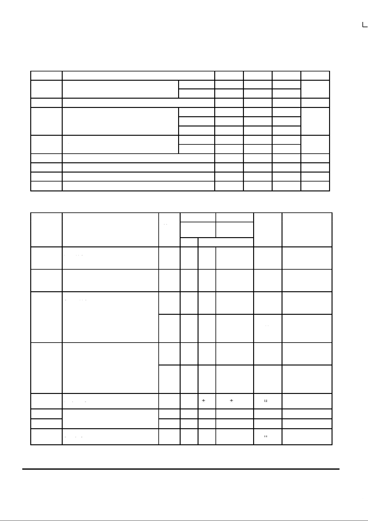
FACT DATA
RECOMMENDED OPERATING CONDITIONS
Symbol Parameter Min Typ Min Unit
′AC 2.0 5.0 6.0
VCCSupply Voltage
′ACT 4.5 5.0 5.5
V
VREG DC Regulated Power Voltage (Ref. to GND) 0 V
CC
V
VCC @ 3.0 V 150
tr, t
f
Input Rise and Fall Time (Note 1)
′AC Devices except Schmitt Inputs
VCC @ 4.5 V 40 ns/V
r
, t
f
′AC Devices except Schmitt Inputs
VCC @ 5.5 V 25
Input Rise and Fall Time (Note 2)
VCC @ 4.5 V 10
tr, t
f
Input Rise and Fall Time (Note 2)
′ACT Devices except Schmitt Inputs
VCC @ 5.5 V 8.0
ns/V
T
J
Junction Temperature (PDIP) 140 °C
T
A
Operating Ambient Temperature Range –40 25 85 °C
I
OH
Output Current — HIGH –24 mA
I
OL
Output Current — LOW 24 mA
1. Vin from 30% to 70% VCC; see individual Data Sheets for devices that differ from the typical input rise and fall times.
2. Vin from 0.8 V to 2.0 V; see individual Data Sheets for devices that differ from the typical input rise and fall times.
DC CHARACTERISTICS
74AC 74AC
Symbol
Parameter
V
CC
(V)
TA = +25°C
TA =
–40°C to +85°C
Unit
Conditions
Typ Guaranteed Limits
V
IH
Minimum High Level
3.0 1.5 2.1 2.1 V
OUT
= 0.1 V
Input Voltage
4.5 2.25 3.15 3.15 V or VCC – 0.1 V
5.5 2.75 3.85 3.85
V
IL
Maximum Low Level
3.0 1.5 0.9 0.9 V
OUT
= 0.1 V
Input Voltage
4.5 2.25 1.35 1.35 V or VCC – 0.1 V
5.5 2.75 1.65 1.65
V
OH
Minimum Low Level
3.0 2.99 2.9 2.9 I
OUT
= – 50 µA
Output Voltage
4.5 4.49 4.4 4.4 V
5.5 5.49 5.4 5.4
*VIN = VIL or V
IH
3.0 2.56 2.46
– 12 mA
4.5 3.86 3.76
V
I
OH
– 24 mA
5.5 4.86 4.76 – 24 mA
V
OL
Maximum Low Level
3.0 0.002 0.1 0.1 I
OUT
= 50 µA
Output Voltage
4.5 0.001 0.1 0.1 V
5.5 0.001 0.1 0.1
*VIN = VIL or V
IH
3.0 0.36 0.44
12 mA
4.5 0.36 0.44
V
I
OL
24 mA
5.5 0.36 0.44 24 mA
I
IN
Maximum Input
VI = VCC, GND
Leakage Current
5.5
±0.1
±1.0
µA
I
= VCC, GND
I
OLD
†Minimum Dynamic
5.5 75 mA V
OLD
= 1.65 V Max
I
OHD
Output Current
5.5 –75 mA V
OHD
= 3.85 V Min
I
CC
Maximum Quiescent
VIN = VCC or GND
Supply Current
5.5
4.040µA
IN
= VCC or GND
* All outputs loaded; thresholds on input associated with output under test.
†Maximum test duration 2.0 ms, one output loaded at a time.
Note: IIN and ICC @ 3.0 V are guaranteed to be less than or equal to the respective limit @ 5.5 V.
 Loading...