

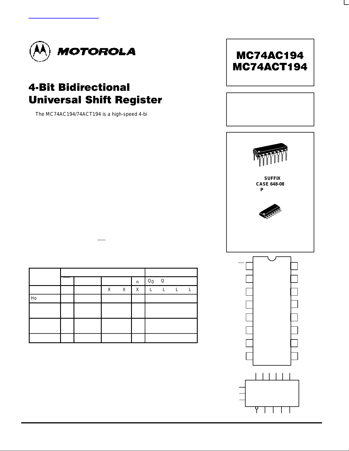
MOTOROLA MC74AC194, MC74ACT194 Technical data
5-1
FACT DATA
The MC74AC194/74ACT194 is a high-speed 4-bit bidirectional universal shift
register. As a high-speed multifunctional, sequential building block, it is useful in
a wide variety of applications. It may be used in serial-serial, shift left, shift right,
serial-parallel, parallel-serial, and parallel-parallel data register transfers. The
′AC/ACT194 is similar in operation to the ′AS195 universal shift register, with
added features of shift left without external connections and hold (do nothing)
modes of operation.
• Typical Shift Frequency of 150 MHz
• Asynchronous Master Reset
• Hold (Do Nothing) Mode
• Fully Synchronous Serial or Parallel Data Transfers
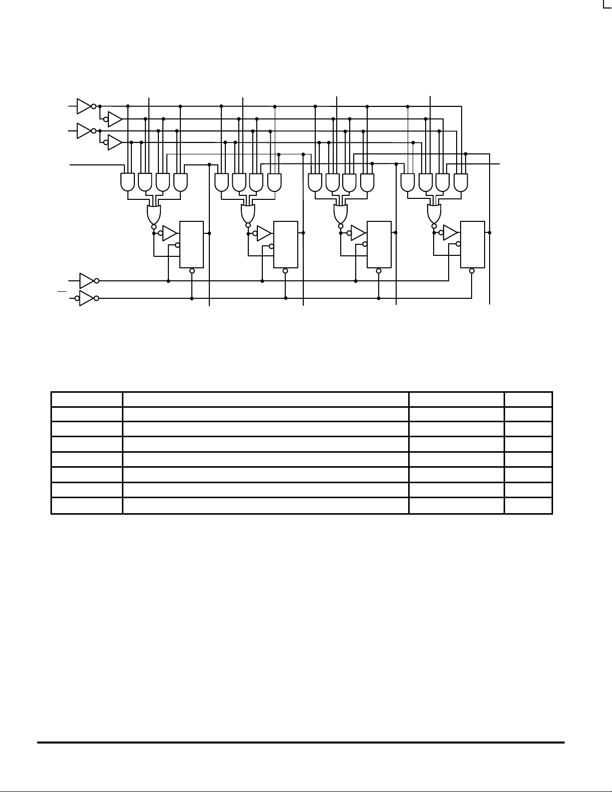
FUNCTIONAL DESCRIPTION
The MC74AC/74ACT194 contains four edge-triggered D flip-flops and the
necessary interstage logic to synchronously perform shift right, shift left, parallel
load and hold operations. Signals applied to the Select (S0, S1) inputs
determine the type of operation, as shown in the Mode Select Table. Signals
on the Select, Parallel data (P0–P3) and Serial data (DSR, DSL) inputs can
change when the clock is in either state, provided only that the recommended
setup and hold times, with respect to the clock rising edge, are observed. A
LOW signal on Master Reset (MR
) overrides all other inputs and forces the
outputs LOW.
MODE SELECT TABLE
Operating
Inputs Outputs
Operating
Mode
MR S1S0D
SRDSLPn
Q0Q1Q2Q
3
Reset L X X X X X L L L L
Hold H l l X X X q0q1q2q
3
H h l X l X q1q2q
3
L
Shift Left
H h l X h X q1q2q3H
H l h l X X L q0q1q
2
Shift Right
H l h h X X H q0q1q
2
Parallel Load H h h X X pnp0p1p2p
3
l = LOW voltage level one setup time prior to the LOW-to-HIGH clock transition.
h = HIGH voltage level one setup time prior to the LOW-to-HIGH clock transition.
Pn (qn) = Lower case letters indicate the state of the referenced input (or output) one setup
time prior to the LOW-to-HIGH clock transition.
H = HIGH Voltage Level
L = LOW Voltage Level
X = Immaterial
4-BIT BIDIRECTIONAL
UNIVERSAL SHIFT
REGISTER
N SUFFIX
CASE 648-08
PLASTIC
D SUFFIX
CASE 751B-05
PLASTIC
1
2 3 4 5 6 7
12131415
9
10
11
MR
CP
S
1
S
0
DSRP0P1P2P3D
SL
Q0Q1Q2Q
3
V
CC
GND
D
SL
P
3
P
2
P
1
15
16
14
12
11
10
2
1
3
4
5
6
7
98
P
0
D
SR
MR
S
0
S
1
CP
Q
3
Q
2
Q
1
Q
0
13
查询MC74AC194供应商
MC74AC194 MC74ACT194
5-2
FACT DATA
D
SR
P
0
P
2
P
3
D
SR
Q
0
Q
1
Q
2
Q
3
CP
S
1
S
0
P
1
MR
CP
R
S Q
0
CLEAR
CP
R
S Q
1
CLEAR
CP
R
S Q
2
CLEAR
CP
R
S Q
3
CLEAR
LOGIC DIAGRAM
Please note that this diagram is provided only for the understanding of logic
operations and should not be used to estimate propagation delays.
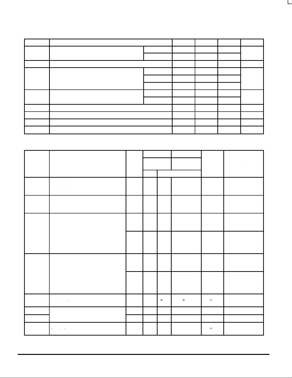
MAXIMUM RATINGS*
Symbol Parameter Value Unit
V
CC
DC Supply Voltage (Referenced to GND) –0.5 to +7.0 V
V
in
DC Input Voltage (Referenced to GND) –0.5 to VCC +0.5 V
V
out
DC Output Voltage (Referenced to GND) –0.5 to VCC +0.5 V
I
in
DC Input Current, per Pin ±20 mA
I
out
DC Output Sink/Source Current, per Pin ±50 mA
I
CC
DC VCC or GND Current per Output Pin ±50 mA
T
stg
Storage Temperature –65 to +150 °C
* Maximum Ratings are those values beyond which damage to the device may occur. Functional operation should be restricted to the Recommended
Operating Conditions.
MC74AC194 MC74ACT194
5-3
FACT DATA
RECOMMENDED OPERATING CONDITIONS
Symbol Parameter Min Typ Max Unit
′AC 2.0 5.0 6.0
VCCSupply Voltage
′ACT 4.5 5.0 5.5
V
Vin, V
out
DC Input Voltage, Output Voltage (Ref. to GND) 0 V
CC
V
VCC @ 3.0 V 150
Input Rise and Fall Time (Note 1)
′AC Devices except Schmitt Inputs
VCC @ 4.5 V 40 ns/V
r
, t
f
′AC Devices except Schmitt Inputs
VCC @ 5.5 V 25
VCC @ 4.5 V 10
tr, t
f
Input Rise and Fall Time (Note 2)
′ACT Devices except Schmitt Inputs
VCC @ 5.5 V 8.0
ns/V
T
J
Junction Temperature (PDIP) 140 °C
T
A
Operating Ambient Temperature Range –40 25 85 °C
I
OH
Output Current — High –24 mA
I
OL
Output Current — Low 24 mA
1. Vin from 30% to 70% VCC; see individual Data Sheets for devices that differ from the typical input rise and fall times.
2. Vin from 0.8 V to 2.0 V; see individual Data Sheets for devices that differ from the typical input rise and fall times.
DC CHARACTERISTICS
74AC 74AC
Symbol
Parameter
V
CC
(V)
TA = +25°C
TA =
–40°C to +85°C
Unit
Conditions
Typ Guaranteed Limits
V
IH
3.0 1.5 2.1 2.1 V
OUT
= 0.1 V
4.5 2.25 3.15 3.15 V or VCC – 0.1 V
5.5 2.75 3.85 3.85
V
IL
3.0 1.5 0.9 0.9 V
OUT
= 0.1 V
4.5 2.25 1.35 1.35 V or VCC – 0.1 V
5.5 2.75 1.65 1.65
V
OH
3.0 2.99 2.9 2.9 I
OUT
= –50 µA
4.5 4.49 4.4 4.4 V
5.5 5.49 5.4 5.4
*VIN = VIL or V
IH
3.0 2.56 2.46
–12 mA
4.5 3.86 3.76
V
I
OH
–24 mA
5.5 4.86 4.76 –24 mA
V
OL
3.0 0.002 0.1 0.1 I
OUT
= 50 µA
4.5 0.001 0.1 0.1 V
5.5 0.001 0.1 0.1
*VIN = VIL or V
IH
3.0 0.36 0.44
12 mA
4.5 0.36 0.44
V
I
OL
24 mA
5.5 0.36 0.44 24 mA
I
IN
5.5
±0.1
±1.0
µA
VI = VCC, GND
I
OLD
5.5 75 mA V
OLD
= 1.65 V Max
I
OHD
Output Current
5.5 –75 mA V
OHD
= 3.85 V Min
I
CC
5.5
8.080µA
VIN = VCC or GND
* All outputs loaded; thresholds on input associated with output under test.
†Maximum test duration 2.0 ms, one output loaded at a time.
Note: IIN and ICC @ 3.0 V are guaranteed to be less than or equal to the respective limit @ 5.5 V VCC.
tr, t
f
Input Rise and Fall Time (Note 2)
Minimum High Level
Input Voltage
Maximum Low Level
Input Voltage
Minimum High Level
Output Voltage
Maximum Low Level
Output Voltage
Maximum Input
Leakage Current
†Minimum Dynamic
Maximum Quiescent
Supply Current
 Loading...