

5-1
FACT DATA
The MC74AC190 is a reversible BCD (8421) decade counter which features
synchronous counting and asynchronous presetting. The preset feature allows
the MC74AC190 to be used in programmable dividers. The Count Enable input,
the Terminal Count output and the Ripple Clock output make possible a variety
of methods of implementing multistage counters. In the counting modes, state
changes are initiated by the rising edge of the clock.
• High-Speed — 120 MHz Typical Count Frequency
• Synchronous Counting
• Asynchronous Parallel Load
• Cascadable
• Outputs Source/Sink 24 mA
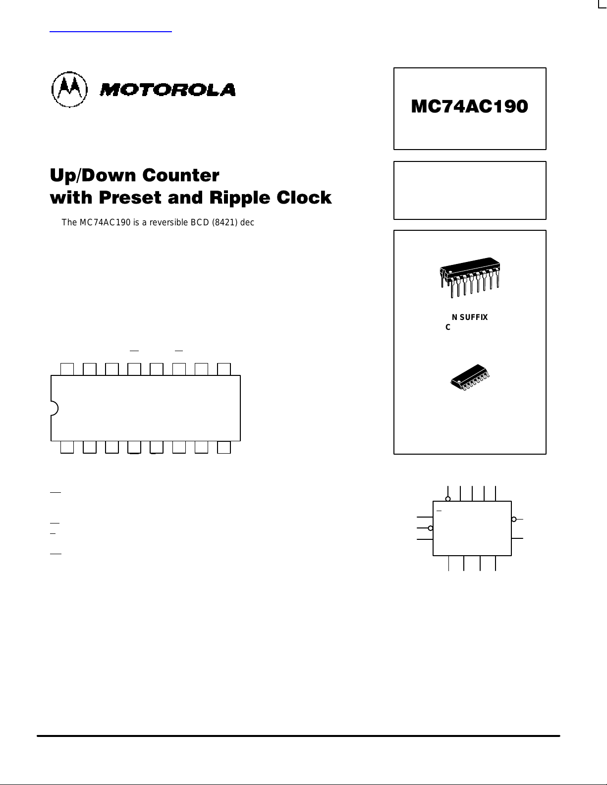
1516 14 13 12 11 10
21 3 4 5 6 7
V
CC
9
8
P0CP RC
TC PL P2P
3
P1Q1Q0CE
U/D Q2Q3GND
PIN NAMES
CE
Count Enable Input
CP Clock Pulse Input
P0–P3Parallel Data Inputs
PL
Asynchronous Parallel Load Input
U
/D Up/Down Count Control Input
Q0–Q3Flip-Flop Outputs
RC
Ripple Clock Output
TC Terminal Count Output
UP/DOWN COUNTER
WITH PRESET
AND RIPPLE CLOCK
N SUFFIX
CASE 648-08
PLASTIC
D SUFFIX
CASE 751B-05
PLASTIC
LOGIC SYMBOL
PL P0P1P2P
3
RC
TC
CE
CP
Q0Q1Q2Q
3
U
/D
查询MC74AC190供应商
MC74AC190
5-2
FACT DATA
FUNCTIONAL DESCRIPTION
The MC74AC190 is a synchronous up/down BCD decade
counter. It contains four edge-triggered flip-flops with internal
gating and steering logic to provide individual preset, count-up
and count-down operations.
Each circuit has an asynchronous parallel load capability
permitting the counter to be preset to any desired number.
When the Parallel Load (PL
) input is LOW, information present
on the Parallel Load inputs (P0–P3) is loaded into the counter
and appears on the Q outputs. This operation overrides the
counting functions, as indicated in the Mode Select Table.
A HIGH signal on the CE
input inhibits counting. When CE
is LOW, internal state changes are initiated synchronously by
the LOW-to-HIGH transition of the clock input. The direction of
counting is determined by the U
/D input signal, as indicated in
the Mode Select Table. CE
and U/D can be changed with the
clock in either state, provided only that the recommended
setup and hold times are observed.
Two types of outputs are provided as overflow/underflow
indicators. The terminal count (TC) output is normally LOW. It
goes HIGH when the circuits reach zero in the count down
mode or 9 in the count up mode. The TC output will then
remain HIGH until a state change occurs, whether by counting
or presetting or until U
/D is changed. The TC output should not
be used as a clock signal because it is subject to decoding
spikes.
The TC signal is also used internally to enable the Ripple
Clock (RC
) output. The RC output is normally HIGH. When CE
is LOW and TC is HIGH, RC output will go LOW when the clock
next goes LOW and will stay LOW until the clock goes HIGH
again. This feature simplifies the design of multistage
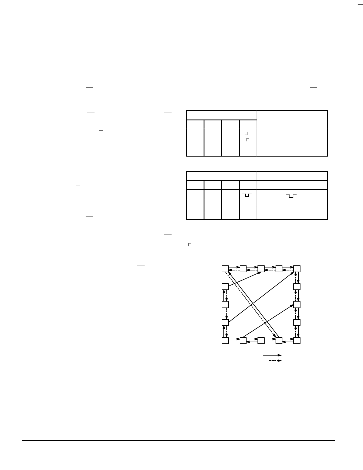
counters, as indicated in Figures a and b. In Figure a, each RC
output is used as the clock input for the next higher stage. This
configuration is particularly advantageous when the clock
source has a limited drive capability, since it drives only the first
stage. To prevent counting in all stages it is only necessary to
inhibit the first stage, since a HIGH signal on CE
inhibits the
RC
output pulse, as indicated in the RC Truth Table. A
disadvantage of this configuration, in some applications, is the
timing skew between state changes in the first and lost stages.
This represents the cumulative delay of the clock as it ripples
through the preceding stages.
A method of causing state changes to occur simultaneously
in all stages is shown in Figure b. All clock inputs are driven in
parallel and the RC
outputs propagate the carry/borrow
signals in ripple fashion. In this configuration the LOW state
duration of the clock must be long enough to allow the
negative-going edge of the carry/borrow signal to ripple
through to the last stage before the clock goes HIGH. There
is no such restriction on the HIGH state duration of the clock,
since the RC
output of any device goes HIGH shortly after its
CP input goes HIGH.
The configuration shown in Figure c avoids ripple delays
and their associated restrictions. The CE
input for a given
stage is formed by combining the TC signals from all the
preceding stages. Note that in order to inhibit counting an
enable signal must be included in each carry gate. The simple
inhibit scheme of Figures a and b doesn’t apply, because the
TC output of a given stage is not affected by its own CE
.
MODE SELECT TABLE
Inputs
PL CE U/D CP
Mode
H L L Count Up
H L H Count Down
L X X X Preset (Asyn.)
H H X X No Change (Hold)
RC TRUTH TABLE
Inputs Output
PL CE TC* CP RC
H L H
H H X X H
H X L X H
L X X X H
*TC is generated internally
H = HIGH Voltage Level
L = LOW Voltage Level
X = Immaterial
= LOW-to-HIGH Transition
COUNT UP
COUNT DOWN
0 1 2 3 4
5
6
7
8
15
14
13
12 11 10 9
STATE DIAGRAM
MC74AC190
5-3
FACT DATA
Figure a: N-Stage Counter Using Ripple Clock
Figure b: Synchronous N-Stage Counter Using Ripple Carry/Borrow
Figure c: Synchronous N-Stage Counter With Parallel Gated Carry/Borrow
DIRECTION
CONTROL
CLOCK
ENABLE
U/D
CE
CP
RC U/D
CE
CP
RC U/D
CE
CP
RC
U/D
CE
CP
RC U/D
CE
CP
RC U/D
CE
CP
RC
DIRECTION
CONTROL
CLOCK
ENABLE
U/D
CE
CP TC
U/D
CE
CP TC
U/D
CE
CP TC
DIRECTION
CONTROL
CLOCK
ENABLE

MC74AC190
5-4
FACT DATA
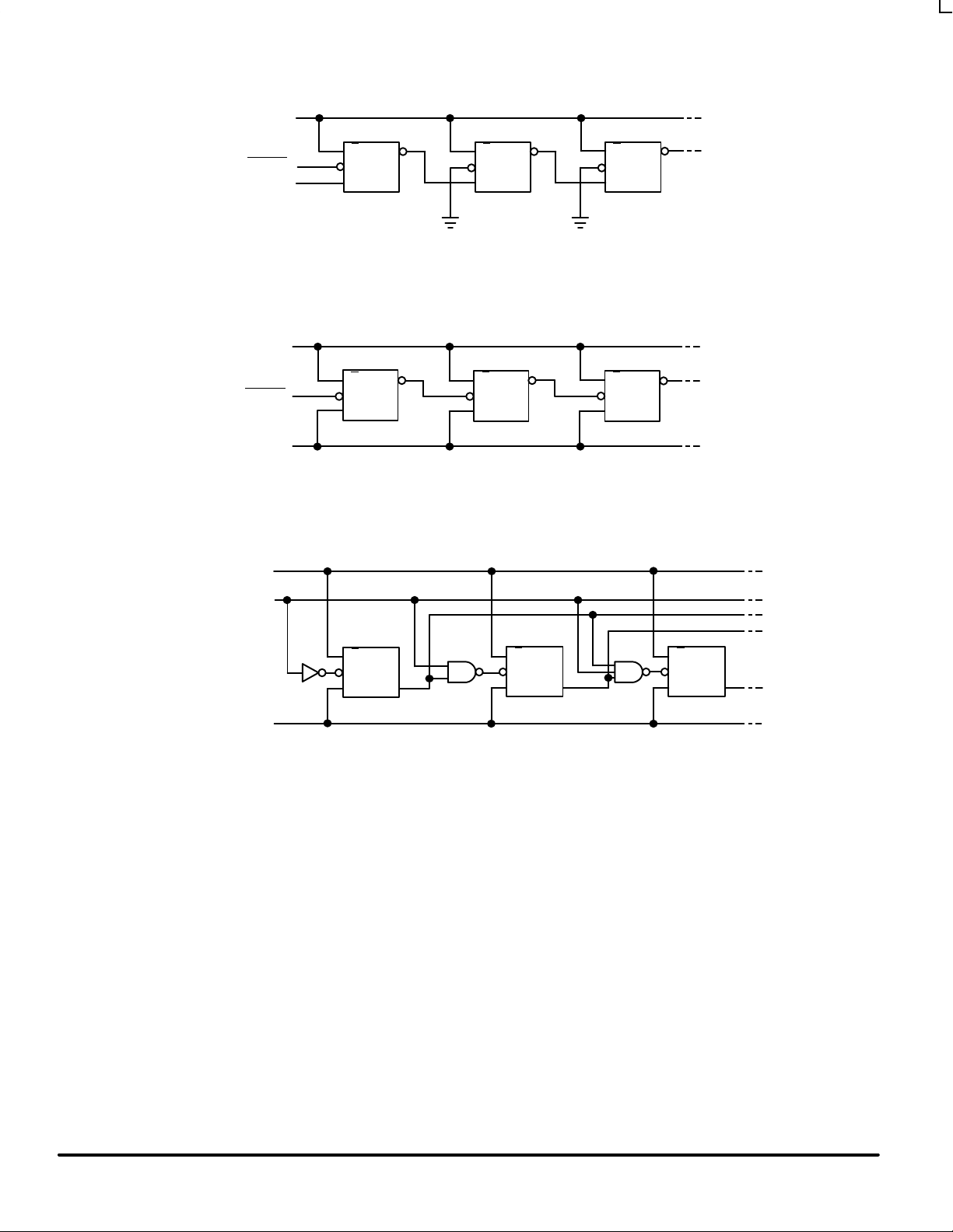
CLOCK
PRESET
CLEAR
Q Q
J K CLOCK
PRESET
CLEAR
Q Q
J K CLOCK
PRESET
CLEAR
Q Q
J K CLOCK
PRESET
CLEAR
Q Q
J K
LOGIC DIAGRAM
CP U/D P
0
CE P
1
P
2
P
3
PL
RC TC
Q
0
Q
1
Q
2
Q
3
Please note that this diagram is provided only for the understanding of logic
operations and should not be used to estimate propagation delays.
MAXIMUM RATINGS*
Symbol Parameter Value Unit
V
CC
DC Supply Voltage (Referenced to GND) –0.5 to +7.0 V
V
in
DC Input Voltage (Referenced to GND) –0.5 to VCC +0.5 V
V
out
DC Output Voltage (Referenced to GND) –0.5 to VCC +0.5 V
I
in
DC Input Current, per Pin ±20 mA
I
out
DC Output Sink/Source Current, per Pin ±50 mA
I
CC
DC VCC or GND Current per Output Pin ±50 mA
T
stg
Storage Temperature –65 to +150 °C
* Maximum Ratings are those values beyond which damage to the device may occur. Functional operation should be restricted to the Recommended
Operating Conditions.

MC74AC190
5-5
FACT DATA
RECOMMENDED OPERATING CONDITIONS
Symbol Parameter Min Typ Max Unit
′AC 2.0 5.0 6.0
VCCSupply Voltage
′ACT 4.5 5.0 5.5
V
Vin, V
out
DC Input Voltage, Output Voltage (Ref. to GND) 0 V
CC
V
VCC @ 3.0 V 150
Input Rise and Fall Time (Note 1)
′AC Devices except Schmitt Inputs
VCC @ 4.5 V 40 ns/V
r
, t
f
′AC Devices except Schmitt Inputs
VCC @ 5.5 V 25
VCC @ 4.5 V 10
tr, t
f
Input Rise and Fall Time (Note 2)
′ACT Devices except Schmitt Inputs
VCC @ 5.5 V 8.0
ns/V
T
J
Junction Temperature (PDIP) 140 °C
T
A
Operating Ambient Temperature Range –40 25 85 °C
I
OH
Output Current — High –24 mA
I
OL
Output Current — Low 24 mA
1. Vin from 30% to 70% VCC; see individual Data Sheets for devices that differ from the typical input rise and fall times.
2. Vin from 0.8 V to 2.0 V; see individual Data Sheets for devices that differ from the typical input rise and fall times.
DC CHARACTERISTICS
74AC 74AC
Symbol
Parameter
V
CC
(V)
TA = +25°C
TA =
–40°C to +85°C
Unit
Conditions
Typ Guaranteed Limits
V
IH
3.0 1.5 2.1 2.1 V
OUT
= 0.1 V
4.5 2.25 3.15 3.15 V or VCC – 0.1 V
5.5 2.75 3.85 3.85
V
IL
3.0 1.5 0.9 0.9 V
OUT
= 0.1 V
4.5 2.25 1.35 1.35 V or VCC – 0.1 V
5.5 2.75 1.65 1.65
V
OH
3.0 2.99 2.9 2.9 I
OUT
= –50 µA
4.5 4.49 4.4 4.4 V
5.5 5.49 5.4 5.4
*VIN = VIL or V
IH
3.0 2.56 2.46
–12 mA
4.5 3.86 3.76
V
I
OH
–24 mA
5.5 4.86 4.76 –24 mA
V
OL
3.0 0.002 0.1 0.1 I
OUT
= 50 µA
4.5 0.001 0.1 0.1 V
5.5 0.001 0.1 0.1
*VIN = VIL or V
IH
3.0 0.36 0.44
12 mA
4.5 0.36 0.44
V
I
OL
24 mA
5.5 0.36 0.44 24 mA
I
IN
5.5
±0.1
±1.0
µA
VI = VCC, GND
I
OLD
5.5 75 mA V
OLD
= 1.65 V Max
I
OHD
Output Current
5.5 –75 mA V
OHD
= 3.85 V Min
I
CC
5.5
8.080µA
VIN = VCC or GND
* All outputs loaded; thresholds on input associated with output under test.
†Maximum test duration 2.0 ms, one output loaded at a time.
Note: IIN and ICC @ 3.0 V are guaranteed to be less than or equal to the respective limit @ 5.5 V VCC.
tr, t
f
Input Rise and Fall Time (Note 2)
Minimum High Level
Input Voltage
Maximum Low Level
Input Voltage
Minimum High Level
Output Voltage
Maximum Low Level
Output Voltage
Maximum Input
Leakage Current
†Minimum Dynamic
Maximum Quiescent
Supply Current

MC74AC190
5-6
FACT DATA
AC CHARACTERISTICS (For Figures and Waveforms — See Section 3)
74AC190 74AC190
Symbol
Parameter
VCC*
(V)
TA = +25°C
CL = 50 pF
TA = –40°C
to +85°C
CL = 50 pF
Unit
Fig.
No.
Min Typ Max Min Max
Maximum Count 3.3 80 MHz 3-3
f
max
Frequency 5.0 110
Propagation Delay 3.3 2.0 1.4 2.0 15.5 ns 3-6
t
PLH
CP to Q
n
5.0 1.5 9.5 2.0 11.0
Propagation Delay 3.3 2.5 14.5 2.0 16.0 ns 3-6
t
PHL
CP to Q
n
5.0 1.5 10.0 2.0 11.5
Propagation Delay 3.3 3.5 17.0 2.0 18.5 ns 3-6
t
PLH
CP to TC 5.0 2.5 11.5 2.0 13.0
Propagation Delay 3.3 3.5 17.0 2.0 18.5 ns 3-6
t
PHL
CP to TC 5.0 2.5 12.5 2.0 13.0
Propagation Delay 3.3 2.5 11.5 2.0 13.0 ns 3-6
t
PLH
CP to RC 5.0 2.0 7.5 2.0 9.5
Propagation Delay 3.3 2.5 11.0 2.0 12.5 ns 3-6
t
PHL
CP to RC 5.0 1.5 8.0 2.0 9.5
Propagation Delay 3.3 2.5 12.0 2.0 13.0 ns 3-6
t
PLH
CE to RC 5.0 1.5 8.0 2.0 9.0
Propagation Delay 3.3 2.0 13.0 2.0 14.5 ns 3-6
t
PHL
CE to RC 5.0 1.5 8.0 2.0 9.0
Propagation Delay 3.3 2.5 14.0 2.0 15.5 ns 3-6
t
PLH
U/D to RC 5.0 1.5 8.5 2.0 10.0
Propagation Delay 3.3 2.5 13.0 2.0 14.5 ns 3-6
t
PHL
U/D to RC 5.0 2.5 8.5 2.0 10.0
Propagation Delay 3.3 3.0 12.0 2.0 13.0 ns 3-6
t
PLH
U/D to TC 5.0 3.0 8.0 2.0 9.0
Propagation Delay 3.3 3.0 12.0 2.0 13.0 ns 3-6
t
PHL
U/D to TC 5.0 3.0 8.0 2.0 9.0
Propagation Delay 3.3 2.0 15.0 1.5 17.0 ns 3-6
t
PLH
Pn to Q
n
5.5 2.0 10.0 1.5 11.5
Propagation Delay 3.3 2.0 14.0 1.5 16.0 ns 3-6
t
PHL
Pn to Q
n
5.0 2.0 9.5 1.5 11.0
Propagation Delay 3.3 3.0 18.0 2.0 19.5 ns 3-6
t
PLH
PL to Q
n
5.0 3.0 10.5 2.0 12.5
Propagation Delay 3.3 2.5 15.0 2.0 17.0 ns 3-6
t
PHL
PL to Q
n
5.0 2.0 10.5 2.0 12.0
* Voltage Range 3.3 V is 3.3 V ±0.3 V.
Voltage Range 5.0 V is 5.0 V ±0.5 V.
MC74AC190
5-7
FACT DATA
AC OPERATING REQUIREMENTS
74AC190 74AC190
Symbol
Parameter
VCC*
(V)
TA = +25°C
CL = 50 pF
TA = –40°C
to +85°C
CL = 50 pF
Unit
Fig.
No.
Typ Guaranteed Minimum
Setup Time, HIGH or LOW 3.3 0.5 0.5 ns 3-9
t
s
Pn to PL 5.0 0 0
Hold Time, HIGH or LOW 3.3 0 0 ns 3-9
t
h
Pn to PL 5.0 0 0
Setup Time, LOW 3.3 6.5 7.5 ns 3-9
t
s
CE to CP 5.0 4.5 5.0
Hold Time, LOW 3.3 0 0 ns 3-9
t
h
CE to CP 5.0 0 0
Setup Time, HIGH or LOW 3.3 8.5 9.5 ns 3-9
t
s
U/D to CP 5.0 5.0 6.0
Hold Time HIGH or LOW 3.3 0 0 ns 3-9
t
h
U/D to CP 5.0 0 0
3.3 5.0 5.5 ns 3-6
twPL Pulse Width, LOW
5.0 3.5 4.0
3.3 5.0 5.5 ns 3-6
twCP Pulse Width, LOW
5.0 3.5 4.0
Recovery Time 3.3 0.5 0.5 ns 3-9
t
rec
PL to CP 5.0 0 0
* Voltage Range 3.3 V is 3.3 V ±0.3 V.
Voltage Range 5.0 V is 5.0 V ±0.5 V.
CAPACITANCE
Symbol Parameter
Value
Typ
Unit Test Conditions
C
IN
Input Capacitance 4.5 pF VCC = 5.0 V
C
PD
Power Dissipation Capacitance 75 pF VCC = 5.0 V

MC74AC190
5-8
FACT DATA
OUTLINE DIMENSIONS
N SUFFIX
PLASTIC DIP PACKAGE
CASE 648–08
ISSUE R
D SUFFIX
PLASTIC SOIC PACKAGE
CASE 751B–05
ISSUE J
NOTES:
1. DIMENSIONING AND TOLERANCING PER
ANSI Y14.5M, 1982.
2. CONTROLLING DIMENSION: MILLIMETER.
3. DIMENSIONS A AND B DO NOT INCLUDE
MOLD PROTRUSION.
4. MAXIMUM MOLD PROTRUSION 0.15 (0.006)
PER SIDE.
5. DIMENSION D DOES NOT INCLUDE DAMBAR
PROTRUSION. ALLOWABLE DAMBAR
PROTRUSION SHALL BE 0.127 (0.005) TOTAL
IN EXCESS OF THE D DIMENSION AT
MAXIMUM MATERIAL CONDITION.
1 8
16 9
SEATING
PLANE
F
J
M
R
X 45
_
G
8 PLP
–B–
–A–
M
0.25 (0.010) B
S
–T–
D
K
C
16 PL
S
B
M
0.25 (0.010) A
S
T
DIM MIN MAX MIN MAX
INCHESMILLIMETERS
A 9.80 10.00 0.386 0.393
B 3.80 4.00 0.150 0.157
C 1.35 1.75 0.054 0.068
D 0.35 0.49 0.014 0.019
F 0.40 1.25 0.016 0.049
G 1.27 BSC 0.050 BSC
J 0.19 0.25 0.008 0.009
K 0.10 0.25 0.004 0.009
M 0 7 0 7
P 5.80 6.20 0.229 0.244
R 0.25 0.50 0.010 0.019
_ _ _ _
NOTES:
1. DIMENSIONING AND TOLERANCING PER ANSI
Y14.5M, 1982.
2. CONTROLLING DIMENSION: INCH.
3. DIMENSION L TO CENTER OF LEADS WHEN
FORMED PARALLEL.
4. DIMENSION B DOES NOT INCLUDE MOLD FLASH.
5. ROUNDED CORNERS OPTIONAL.
–A–
B
F
C
S
H
G
D
J
L
M
16 PL
SEATING
1 8
916
K
PLANE
–T–
M
A
M
0.25 (0.010) T
DIM MIN MAX MIN MAX
MILLIMETERSINCHES
A 0.740 0.770 18.80 19.55
B 0.250 0.270 6.35 6.85
C 0.145 0.175 3.69 4.44
D 0.015 0.021 0.39 0.53
F 0.040 0.70 1.02 1.77
G 0.100 BSC 2.54 BSC
H 0.050 BSC 1.27 BSC
J 0.008 0.015 0.21 0.38
K 0.110 0.130 2.80 3.30
L 0.295 0.305 7.50 7.74
M 0 10 0 10
S 0.020 0.040 0.51 1.01
____
How to reach us:
USA/EUROPE: Motorola Literature Distribution; JAPAN: Nippon Motorola Ltd.; Tatsumi–SPD–JLDC, Toshikatsu Otsuki,
P.O. Box 20912; Phoenix, Arizona 85036. 1–800–441–2447 6F Seibu–Butsuryu–Center, 3–14–2 Tatsumi Koto–Ku, Tokyo 135, Japan. 03–3521–8315
MFAX: RMFAX0@email.sps.mot.com –TOUCHTONE (602) 244–6609 HONG KONG: Motorola Semiconductors H.K. Ltd.; 8B Tai Ping Industrial Park,
INTERNET: http://Design–NET.com 51 Ting Kok Road, Tai Po, N.T., Hong Kong. 852–26629298
Motorola reserves the right to make changes without further notice to any products herein. Motorola makes no warranty , representation or guarantee regarding
the suitability of its products for any particular purpose, nor does Motorola assume any liability arising out of the application or use of any product or circuit, and
specifically disclaims any and all liability , including without limitation consequential or incidental damages. “Typical” parameters can and do vary in different
applications. All operating parameters, including “T ypicals” must be validated for each customer application by customer’s technical experts. Motorola does
not convey any license under its patent rights nor the rights of others. Motorola products are not designed, intended, or authorized for use as components in
systems intended for surgical implant into the body, or other applications intended to support or sustain life, or for any other application in which the failure of
the Motorola product could create a situation where personal injury or death may occur. Should Buyer purchase or use Motorola products for any such
unintended or unauthorized application, Buyer shall indemnify and hold Motorola and its officers, employees, subsidiaries, affiliates, and distributors harmless
against all claims, costs, damages, and expenses, and reasonable attorney fees arising out of, directly or indirectly, any claim of personal injury or death
associated with such unintended or unauthorized use, even if such claim alleges that Motorola was negligent regarding the design or manufacture of the part.
Motorola and are registered trademarks of Motorola, Inc. Motorola, Inc. is an Equal Opportunity/Affirmative Action Employer.
MC74AC190/D
*MC74AC190/D*
◊
 Loading...