

MOTOROLA MC74ACT157ML1, MC74ACT157DT, MC74ACT157DTEL, MC74ACT157DTR2, MC74ACT157M Datasheet
...
5-1
FACT DATA
The MC74AC157/74ACT157 is a high-speed quad 2-input multiplexer. Four
bits of data from two sources can be selected using the common Select and Enable
inputs. The four outputs present the selected data in the true (noninverted) form.
The MC74AC157/74ACT157 can also be used as a function generator.
• Outputs Source/Sink 24 mA
• ′ACT157 Has TTL Compatible Inputs
1516 14 13 12 11 10
21 3 4 5 6 7
V
CC
9
8
E
I0cI
1cZcI0dI1dZd
S I
0aI1aZaI0bI1bZb
GND
PIN NAMES
I0a–I0dSource 0 Data Inputs
I1a–I1dSource 1 Data Inputs
E Enable Input
S Select Input
Za–ZdOutputs
TRUTH TABLE
Inputs Outputs
E S I
0I1
Z
H X X X L
L H X L L
L H X H H
L L L X L
L L H X H
H = HIGH Voltage Level
L = LOW Voltage Level
X = Immaterial
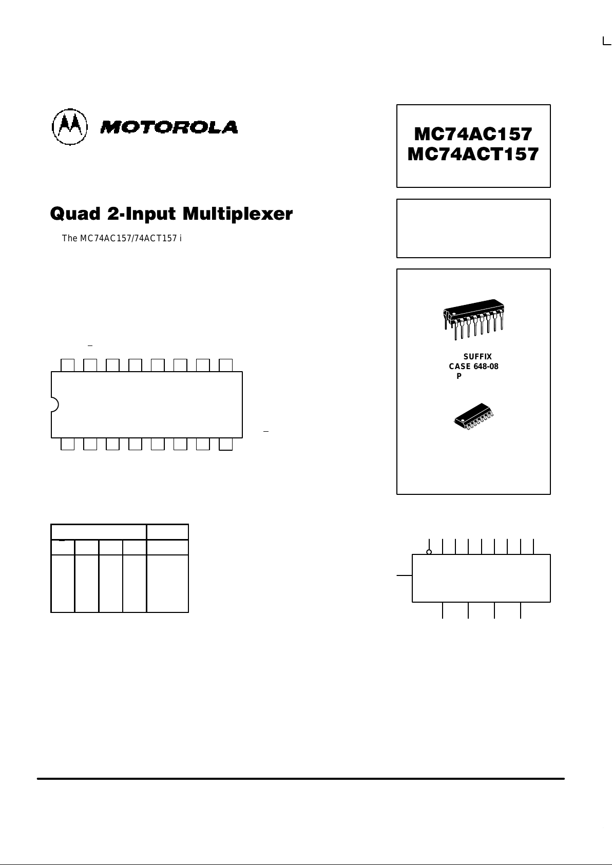
QUAD 2-INPUT
MULTIPLEXER
N SUFFIX
CASE 648-08
PLASTIC
D SUFFIX
CASE 751B-05
PLASTIC
LOGIC SYMBOL
S
E I0aI1aI0bI
1b
Z
b
I0cI1cI0dI
1d
Z
a
Z
c
Z
d
MC74AC157 MC74ACT157
5-2
FACT DATA
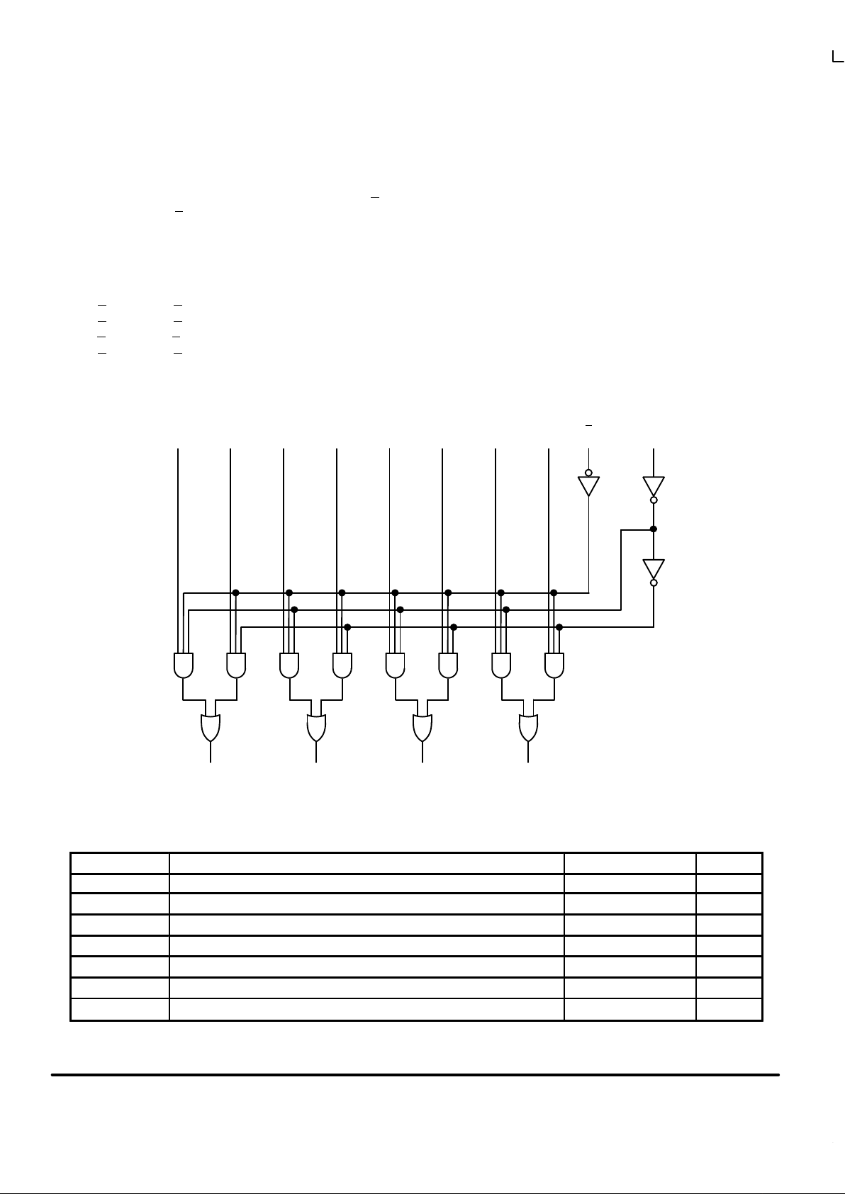
FUNCTIONAL DESCRIPTION
The MC74AC157/74ACT157 is a quad 2-input multiplexer.
It selects four bits of data from two sources under the control
of a common Select input (S). The Enable input (E
) is
active-LOW. When E
is HIGH, all of the outputs (Z) are forced
LOW regardless of all other inputs. The MC74AC157/
74ACT157 is the logic implementation of a 4-pole, 2-position
switch where the position of the switch is determined by the
logic levels supplied to the Select input. The logic equations for
the outputs are shown below:
Za = E
•(I1a•S+I0a•S)
Zb = E
•(I1b•S+I0b•S)
Zc = E
•(I1c•S+I0c•S)
Zd = E
•(I1d•S+I0d•S)
A common use of the MC74AC157/74ACT157 is the
moving of data from two groups of registers to four common
output busses. The particular register from which the data
comes is determined by the state of the Select input. A less
obvious use is as a function generator. The MC74AC157/
74ACT157 can generate any four of the sixteen different
functions of two variables with one variable common. This is
useful for implementing gating functions.
LOGIC DIAGRAM
I
0a
I
1a
I
0b
I
1b
I
0c
I
1c
I
0d
I
1d
E S
Z
a
Please note that this diagram is provided only for the understanding of logic
operations and should not be used to estimate propagation delays.
Z
b
Z
c
Z
d
MAXIMUM RATINGS*
Symbol Parameter Value Unit
V
CC
DC Supply Voltage (Referenced to GND) –0.5 to +7.0 V
V
in
DC Input Voltage (Referenced to GND) –0.5 to VCC +0.5 V
V
out
DC Output Voltage (Referenced to GND) –0.5 to VCC +0.5 V
I
in
DC Input Current, per Pin ±20 mA
I
out
DC Output Sink/Source Current, per Pin ±50 mA
I
CC
DC VCC or GND Current per Output Pin ±50 mA
T
stg
Storage Temperature –65 to +150 °C
* Maximum Ratings are those values beyond which damage to the device may occur. Functional operation should be restricted to the Recommended
Operating Conditions.
 Loading...