

MOTOROLA MC74AC151, MC74ACT151 Technical data
5-1
FACT DATA
The MC74AC151/74ACT151 is a high-speed 8-input digital multiplexer. It
provides, in one package, the ability to select one line of data from up to eight
sources. The MC74AC151/74ACT151 can be used as a universal function
generator to generate any logic function of four variables. Both true and
complementary outputs are provided.
• Outputs Source/Sink 24 mA
• ′ACT151 Has TTL Compatible Inputs
GND
1516 14 13 12 11 10
21 3 4 5 6 7
V
CC
9
8
E
EZZI
0
I
1
I
2
I
3
I4I
5I6I7S0S1S2
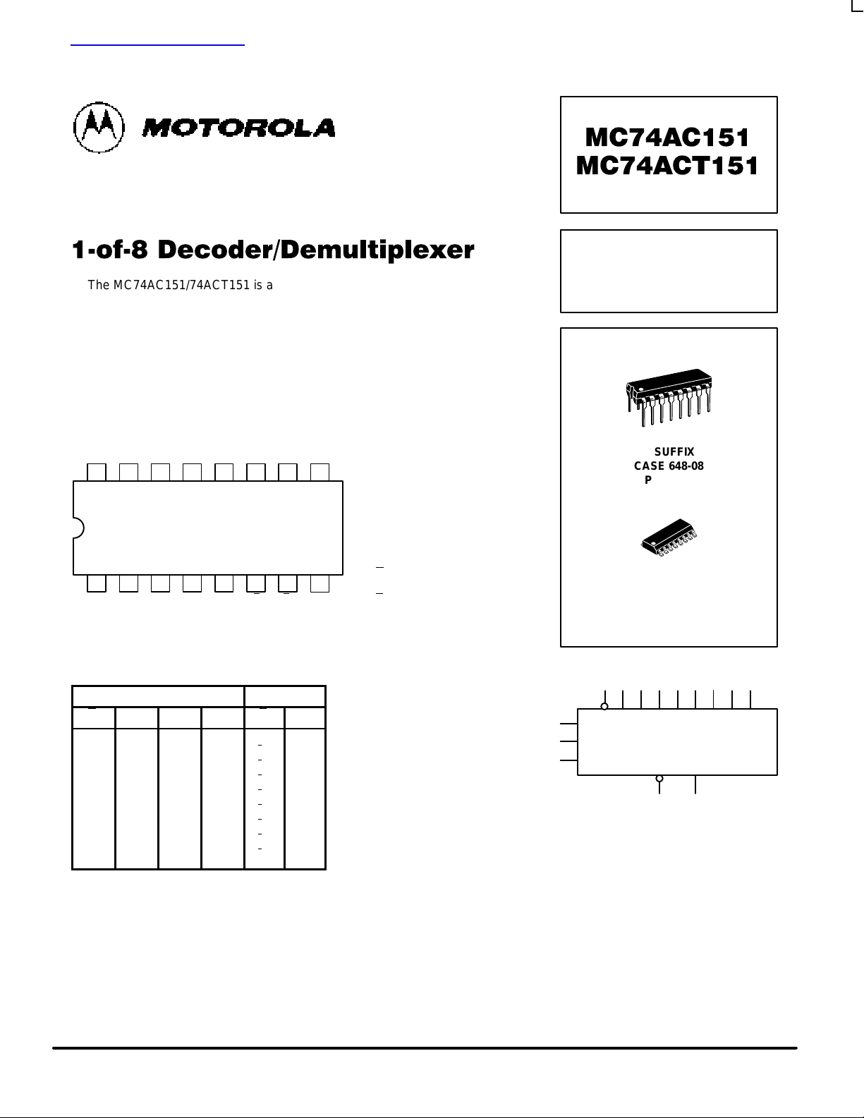
PIN NAMES
I0–I
7
Data Inputs
S0–S2Select Inputs
E
Enable Input
Z Data Output
Z
Inverted Data Output
TRUTH TABLE
Inputs Outputs
E S
2
S
1
S
0
Z Z
H X X X H L
L L L L I
0
I
0
L L L H I
1
I
1
L L H L I
2
I
2
L L H H I
3
I
3
L H L L I
4
I
4
L H L H I
5
I
5
L H H L I
6
I
6
L H H H I
7
I
7
H = HIGH Voltage Level
L = LOW Voltage Level
X = Immaterial
1-OF-8
DECODER/DEMULTIPLEXER
N SUFFIX
CASE 648-08
PLASTIC
D SUFFIX
CASE 751B-05
PLASTIC
LOGIC SYMBOL
S
0
S
1
S
2
Z Z
E I0I1I2I3I4I5I6I
7
查询MC74AC151供应商
MC74AC151 MC74ACT151
5-2
FACT DATA
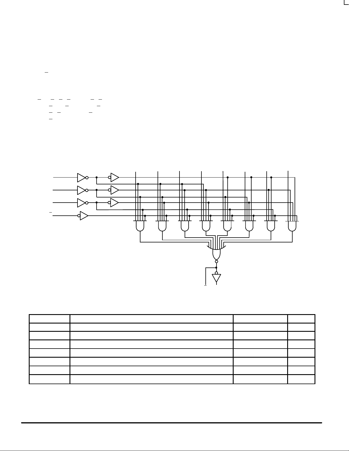
FUNCTIONAL DESCRIPTION
The MC74AC151/74ACT151 is a logic implementation of
a single pole, 8-position switch with the switch position
controlled by the state of three Select inputs, S0, S1, S2. Both
true and complementary outputs are provided. The Enable
input (E
) is active LOW. When it is not activated, the
complementary output is HIGH and the true output is LOW
regardless of all other inputs. The logic function provided at the
output is:
Z = E
•(I0•S0•S1•S
2+I1
•S0•S1•S
2
+
I
2
•S0•S1•S
2+I3
•S0•S1•S
2
+
I
4
•S0•S1•S
2+I5•S0
•S1•S
2
+
I
6
•S0•S1•S
2+I7•S0•S1•S2
)
The MC74AC151/74ACT151 provides the ability, in one
package, to select from eight sources of data or control
information. By proper manipulation of the inputs, the
MC74AC151/74ACT151 can provide any logic function of four
variables and its complement.
Z Z
S
2
S
1
S
0
E
I
0
I
1
I
2
I
3
I
4
I
5
I
6
I
7
LOGIC DIAGRAM
Please note that this diagram is provided
only for the understanding of logic
operations and should not be used to
estimate propagation delays.
MAXIMUM RATINGS*
Symbol Parameter Value Unit
V
CC
DC Supply Voltage (Referenced to GND) –0.5 to +7.0 V
V
in
DC Input Voltage (Referenced to GND) –0.5 to VCC +0.5 V
V
out
DC Output Voltage (Referenced to GND) –0.5 to VCC +0.5 V
I
in
DC Input Current, per Pin ±20 mA
I
out
DC Output Sink/Source Current, per Pin ±50 mA
I
CC
DC VCC or GND Current per Output Pin ±50 mA
T
stg
Storage Temperature –65 to +150 °C
* Maximum Ratings are those values beyond which damage to the device may occur. Functional operation should be restricted to the Recommended
Operating Conditions.
 Loading...