

MOTOROLA MC74AC138, MC74ACT138 Technical data
5-1
FACT DATA
The MC74AC138/74ACT138 is a high-speed 1-of-8 decoder/demultiplexer. This
device is ideally suited for high-speed bipolar memory chip select address decoding.
The multiple input enables allow parallel expansion to a 1-of-24 decoder using just
three MC74AC138/74ACT138 devices or a 1-of-32 decoder using four MC74AC138/
74ACT138 devices and one inverter.
• Demultiplexing Capability
• Multiple Input Enable for Easy Expansion
• Active LOW Mutually Exclusive Outputs
• Outputs Source/Sink 24 mA
• ′ACT138 Has TTL Compatible Inputs
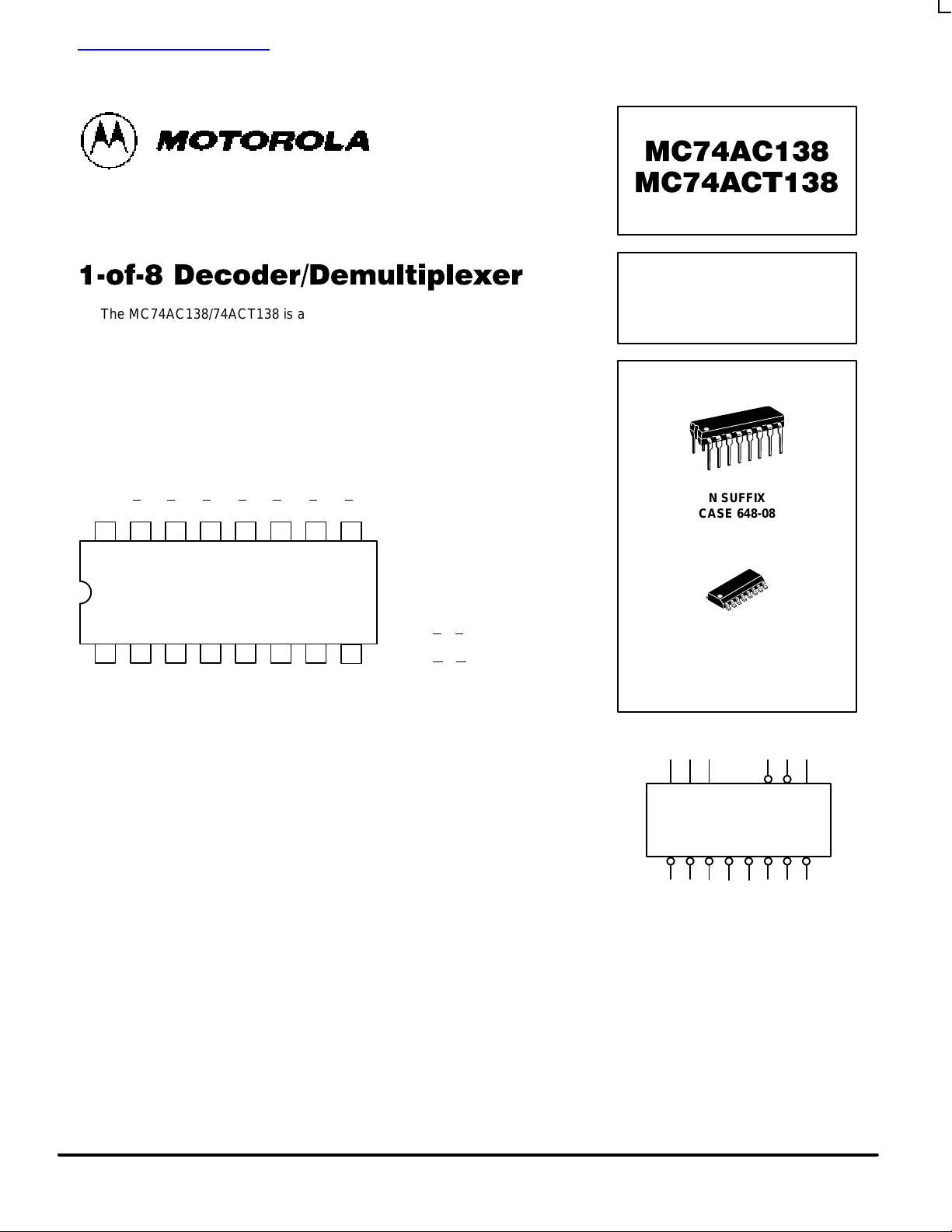
V
CC
GNDA0A1A2E
1E2E3
1516 14 13 12 11 10
21 3 4 5 6 7
9
8
O
7
O
0O1O2O3O4O5O6
PIN NAMES
A0–A2Address Inputs
E
1–E2
Enable Inputs
E
3
Enable Input
O
0–O7
Outputs
1-OF-8 DECODER/
DEMULTIPLEXER
N SUFFIX
CASE 648-08
PLASTIC
D SUFFIX
CASE 751B-05
PLASTIC
LOGIC SYMBOL
A0A1A
2
E1E2E
3
O1O2O3O4O5O6O
7
O
0
查询MC74AC138供应商
MC74AC138 MC74ACT138
5-2
FACT DATA
FUNCTIONAL DESCRIPTION
The MC74AC138/74ACT138 high-speed 1-of-8 decoder/
demultiplexer accepts three binary weighted inputs (A0, A1,
A2) and, when enabled, provides eight mutually exclusive
active-LOW outputs (O
0–O7
). The MC74AC138/74ACT138
features three Enable inputs, two active-LOW (E
1
, E2) and one
active-HIGH (E3). All outputs will be HIGH unless E
1
and E
2
are LOW and E3 is HIGH. This multiple enabled function
allows easy parallel expansion of the device to a 1-of-32 (5
lines to 32 lines) decoder with just four MC74AC138/
74ACT138 devices and one inverter (See Figure a). The
MC74AC138/74ACT138 can be used as an 8-output
demultiplexer by using one of the active LOW Enable inputs
as the data input and the other Enable inputs as strobes. The
Enable inputs which are not used must be permanently tied to
their appropriate active-HIGH or active-LOW state.
TRUTH TABLE
Inputs Outputs
E
1
E
2
E
3
A0A
1
A2O0O1O2O3O4O5O6O
7
H X X X X X H H H H H H H H
X H X X X X H H H H H H H H
X X L X X X H H H H H H H H
L L H L L L L H H H H H H H
L L H H L L H L H H H H H H
L L H L H L H H L H H H H H
L L H H H L H H H L H H H H
L L H L L H H H H H L H H H
L L H H L H H H H H H L H H
L L H L H H H H H H H H L H
L L H H H H H H H H H H H L
H = HIGH Voltage Level
L = LOW Voltage Level
X = Immaterial
A2A
1
A
0
E
3
E
1E2
0
7
0
6
0
5
0
4
0
3
0
2
0
1
0
0
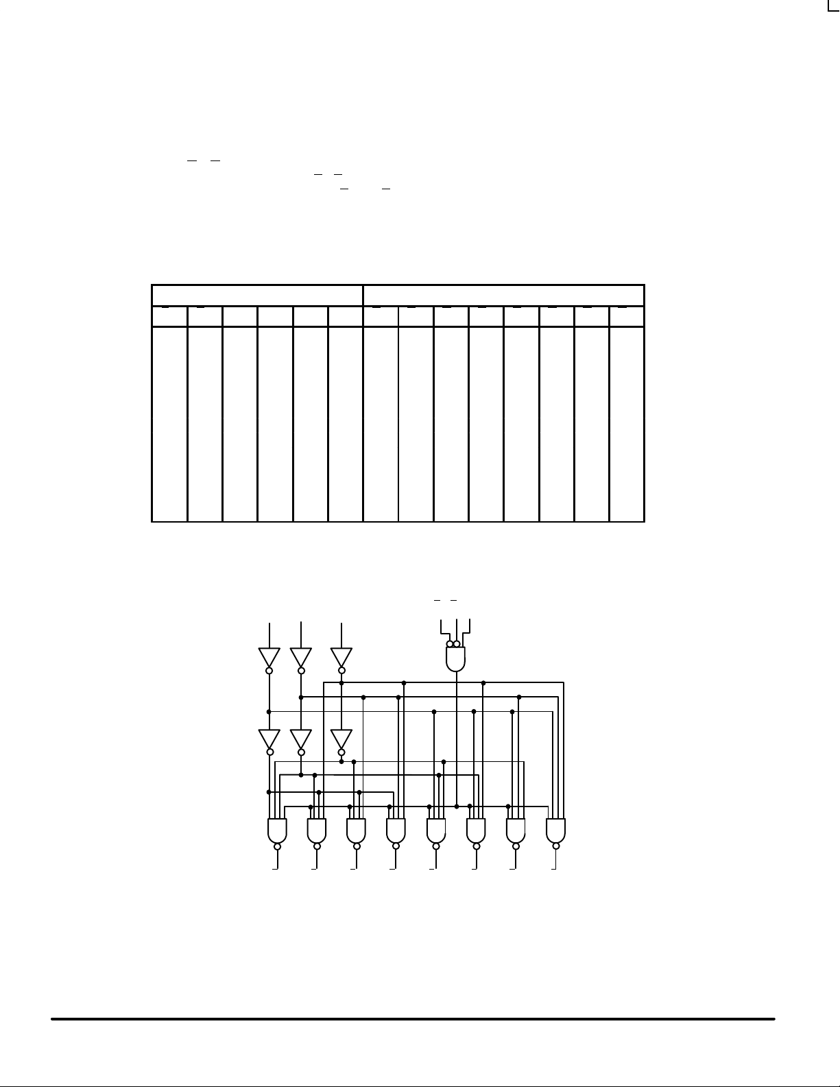
LOGIC DIAGRAM
Please note that this diagram is provided only for the understanding of logic
operations and should not be used to estimate propagation delays.
MC74AC138 MC74ACT138
5-3
FACT DATA
H
123 123 123 123
A
0
A
2
A
3
A
4
A0A1A
2
E
000102030405060
7
A0A1A
2
E
000102030405060
7
A0A1A
2
E
000102030405060
7
A0A1A
2
E
000102030405060
7
0
0
0
31
′
04
Figure a: Expansion to 1-of-32 Decoding
A
1
MAXIMUM RATINGS*
Symbol Parameter Value Unit
V
CC
DC Supply Voltage (Referenced to GND) –0.5 to +7.0 V
V
in
DC Input Voltage (Referenced to GND) –0.5 to VCC +0.5 V
V
out
DC Output Voltage (Referenced to GND) –0.5 to VCC +0.5 V
I
in
DC Input Current, per Pin ±20 mA
I
out
DC Output Sink/Source Current, per Pin ±50 mA
I
CC
DC VCC or GND Current per Output Pin ±50 mA
T
stg
Storage Temperature –65 to +150 °C
* Maximum Ratings are those values beyond which damage to the device may occur. Functional operation should be restricted to the Recommended
Operating Conditions.
RECOMMENDED OPERATING CONDITIONS
Symbol Parameter Min Typ Max Unit
′AC 2.0 5.0 6.0
VCCSupply Voltage
′ACT 4.5 5.0 5.5
V
Vin, V
out
DC Input Voltage, Output Voltage (Ref. to GND) 0 V
CC
V
VCC @ 3.0 V 150
Input Rise and Fall Time (Note 1)
′AC Devices except Schmitt Inputs
VCC @ 4.5 V 40 ns/V
r
, t
f
′AC Devices except Schmitt Inputs
VCC @ 5.5 V 25
VCC @ 4.5 V 10
tr, t
f
Input Rise and Fall Time (Note 2)
′ACT Devices except Schmitt Inputs
VCC @ 5.5 V 8.0
ns/V
T
J
Junction Temperature (PDIP) 140 °C
T
A
Operating Ambient Temperature Range –40 25 85 °C
I
OH
Output Current — High –24 mA
I
OL
Output Current — Low 24 mA
1. Vin from 30% to 70% VCC; see individual Data Sheets for devices that differ from the typical input rise and fall times.
2. Vin from 0.8 V to 2.0 V; see individual Data Sheets for devices that differ from the typical input rise and fall times.
tr, t
f
Input Rise and Fall Time (Note 2)
 Loading...