


查询68HC912DG128CPV8供应商
Freescale Semiconductor, Inc.
MC68HC912DG128
nc...
I
Technical Data
cale Semiconductor,
Frees
M68HC12
Microcontrollers
MOTOROLA.COM/SEMICONDUCTORS
MC68HC912DG128/D
Rev. 3, 10/2002
For More Information On This Product,
Go to: www.freescale.com

Freescale Semiconductor, Inc.
nc...
I
cale Semiconductor,
Frees
For More Information On This Product,
Go to: www.freescale.com

Freescale Semiconductor, Inc.
MC68HC912DG128
Technical Data — Rev 3.0
nc...
I
cale Semiconductor,
Frees
Motorola reserves the righ t to make changes without further notice to any products
herein. Motorola makes no warranty, representation or guarantee regarding the
suitability of i ts products for any partic ular purpose, nor does Moto rola assume any
liability arising out of the application or use of any prod uct or circuit, and s pecifically
disclaims any an d all liability, including withou t limitation consequential or inc idental
damages. "Typical" parameters which may be provided in Motorola data sheets and/or
specifications can an d do vary in different applications and actua l performance may
vary over time. A ll operating parameters, i ncluding "Typicals" must be validated for
each customer application by customer’s technical experts. Motorola does not convey
any license under i ts patent rights nor the rig hts of others. Motorola prod ucts are not
designed, intended, or authorized for use as components in systems intended for
surgical implant into the body, or other applications intended to support or sustain life,
or for any other applicat ion in wh ich the failure of the Mo torola pr oduct could cr eate a
situation where personal injury or death may oc cur. Should Buyer purchase o r use
Motorola products for any such unintended or una uthorized application, Buye r shall
indemnify and hold Motorola and its officers, employees, subsid iaries, affiliates, and
distributors harmless against all claims, costs, damages, and expenses, and
reasonable attorney fees arising out of, directly or indirectly, any claim of personal
injury or death associated with such unintended or unauthorized use, even if such claim
alleges that Motorola was negligent reg arding the design o r manufacture of the p art.
Motorola, Inc. is an Equal Opportunity/Affirmative Action Employer.
Motorola and are registered trademarks of Motorola, Inc.
DigitalDNA is a trademark of Motorola, Inc. © Motorola, Inc., 2002
MC68HC912DG128 — Rev 3.0 Technical Data
MOTOROLA 3
For More Information On This Product,
Go to: www.freescale.com

Freescale Semiconductor, Inc.
nc...
I
cale Semiconductor,
Frees
Technical Data MC68HC912DG128 — Rev 3.0
4 MOTOROLA
For More Information On This Product,
Go to: www.freescale.com

Freescale Semiconductor, Inc.
Technical Data — MC68HC912DG128
List of Paragraphs. . . . . . . . . . . . . . . . . . . . . . . . . . . . . . . .5
Table of Contents . . . . . . . . . . . . . . . . . . . . . . . . . . . . . . . .7
List of Figures . . . . . . . . . . . . . . . . . . . . . . . . . . . . . . . . . .15
List of Paragraphs
nc...
I
cale Semiconductor,
Frees
List of Tables. . . . . . . . . . . . . . . . . . . . . . . . . . . . . . . . . . .19
Section 1. General Description . . . . . . . . . . . . . . . . . . . .23
Section 2. Central Processing Unit . . . . . . . . . . . . . . . . .29
Section 3. Pinout and Signal Descriptions . . . . . . . . . . .37
Section 4. Registers . . . . . . . . . . . . . . . . . . . . . . . . . . . . .63
Section 5. Operating Modes. . . . . . . . . . . . . . . . . . . . . . .75
Section 6. Bus Control and Input/Output . . . . . . . . . . . .95
Section 7. Flash Memory . . . . . . . . . . . . . . . . . . . . . . . .107
Section 8. EEPROM Memory . . . . . . . . . . . . . . . . . . . . .125
Section 9. Resets and Interrupts. . . . . . . . . . . . . . . . . .133
Section 10. I/O Ports with Key Wake-up . . . . . . . . . . . .147
Section 11. Clock Functio ns . . . . . . . . . . . . . . . . . . . . .155
Section 12. Pulse Width Modulator . . . . . . . . . . . . . . . .191
Section 13. Enhanced Capture Timer . . . . . . . . . . . . . .207
Section 14. Multiple Serial Interface . . . . . . . . . . . . . . .249
Section 15. Inter-IC Bus . . . . . . . . . . . . . . . . . . . . . . . . .273
Section 16. Analog-to-Digital Converter . . . . . . . . . . . .297
MC68HC912DG128 — Rev 3.0 Technical Data
MOTOROLA List of Paragraphs 5
For More Information On This Product,
Go to: www.freescale.com

List of Paragraphs
nc...
I
Freescale Semiconductor, Inc.
Section 17. MSCAN Controller. . . . . . . . . . . . . . . . . . . .311
Section 18. Development Support. . . . . . . . . . . . . . . . .355
Section 19. Electrical Specificatio ns. . . . . . . . . . . . . . .385
Section 20. Appendix: CGM Practical Aspects . . . . . .407
Section 21. Appendix: MC68HC912DG128A Flash . . .419
Section 22. Appendix: MC68HC912DG128A EEPROM 427
Section 23. Revision History . . . . . . . . . . . . . . . . . . . . .439
Glossary. . . . . . . . . . . . . . . . . . . . . . . . . . . . . . . . . . . . . .441
cale Semiconductor,
Frees
Technical Data MC68HC912DG128 — Rev 3.0
6 List of Paragraphs MOTOROLA
For More Information On This Product,
Go to: www.freescale.com

Freescale Semiconductor, Inc.
Technical Data — MC68HC912DG128
Table of Contents
List of Paragraphs
Table of Contents
nc...
I
cale Semiconductor,
Frees
List of Figures
List of Tables
Section 1. General Description
1.1 Contents. . . . . . . . . . . . . . . . . . . . . . . . . . . . . . . . . . . . . . . . . .23
1.2 Introduction. . . . . . . . . . . . . . . . . . . . . . . . . . . . . . . . . . . . . . . . 23
1.3 Features . . . . . . . . . . . . . . . . . . . . . . . . . . . . . . . . . . . . . . . . . .24
1.4 Ordering Information. . . . . . . . . . . . . . . . . . . . . . . . . . . . . . . . . 27
1.5 MC68HC912DG128 Block Diagram. . . . . . . . . . . . . . . . . . . . .28
Section 2. Central Processing Unit
2.1 Contents. . . . . . . . . . . . . . . . . . . . . . . . . . . . . . . . . . . . . . . . . .29
2.2 Introduction. . . . . . . . . . . . . . . . . . . . . . . . . . . . . . . . . . . . . . . . 29
2.3 Programming Model. . . . . . . . . . . . . . . . . . . . . . . . . . . . . . . . .29
2.4 Data Types. . . . . . . . . . . . . . . . . . . . . . . . . . . . . . . . . . . . . . . .31
2.5 Addressing Modes . . . . . . . . . . . . . . . . . . . . . . . . . . . . . . . . . .31
2.6 Indexed Addressing Modes . . . . . . . . . . . . . . . . . . . . . . . . . . .34
2.7 Opcodes and Operands . . . . . . . . . . . . . . . . . . . . . . . . . . . . . .35
MC68HC912DG128 — Rev 3.0 Technical Data
MOTOROLA Table of Contents 7
For More Information On This Product,
Go to: www.freescale.com

Table of Contents
Freescale Semiconductor, Inc.
Section 3. Pinout and Signal Descriptions
3.1 Contents. . . . . . . . . . . . . . . . . . . . . . . . . . . . . . . . . . . . . . . . . .37
3.2 Pin Assignments in 112-pin QFP . . . . . . . . . . . . . . . . . . . . . . .37
3.3 Power Supply Pins . . . . . . . . . . . . . . . . . . . . . . . . . . . . . . . . . .40
3.4 Signal Descriptions. . . . . . . . . . . . . . . . . . . . . . . . . . . . . . . . . .42
3.5 Port Signals . . . . . . . . . . . . . . . . . . . . . . . . . . . . . . . . . . . . . . .51
Section 4. Registers
nc...
I
cale Semiconductor,
Frees
4.1 Contents. . . . . . . . . . . . . . . . . . . . . . . . . . . . . . . . . . . . . . . . . .63
4.2 Register Block. . . . . . . . . . . . . . . . . . . . . . . . . . . . . . . . . . . . . .63
Section 5. Operating Modes
5.1 Contents. . . . . . . . . . . . . . . . . . . . . . . . . . . . . . . . . . . . . . . . . .75
5.2 Introduction. . . . . . . . . . . . . . . . . . . . . . . . . . . . . . . . . . . . . . . . 75
5.3 Operating Modes . . . . . . . . . . . . . . . . . . . . . . . . . . . . . . . . . . .75
5.4 Background Debug Mode. . . . . . . . . . . . . . . . . . . . . . . . . . . . .78
5.5 Internal Resource Mapping. . . . . . . . . . . . . . . . . . . . . . . . . . . .81
5.6 Memory Maps. . . . . . . . . . . . . . . . . . . . . . . . . . . . . . . . . . . . . .93
Section 6. Bus Control and Input/Output
6.1 Contents. . . . . . . . . . . . . . . . . . . . . . . . . . . . . . . . . . . . . . . . . .95
6.2 Introduction. . . . . . . . . . . . . . . . . . . . . . . . . . . . . . . . . . . . . . . . 95
6.3 Detecting Access Type from External Signals . . . . . . . . . . . . .95
6.4 Registers. . . . . . . . . . . . . . . . . . . . . . . . . . . . . . . . . . . . . . . . . .96
Section 7. Flash Memory
7.1 Contents. . . . . . . . . . . . . . . . . . . . . . . . . . . . . . . . . . . . . . . . .107
7.2 Introduction. . . . . . . . . . . . . . . . . . . . . . . . . . . . . . . . . . . . . . . 1 07
Technical Data MC68HC912DG128 — Rev 3.0
8 Table of Conten ts MOTOROLA
For More Information On This Product,
Go to: www.freescale.com

Freescale Semiconductor, Inc.
7.3 Future Flash EEPROM Support. . . . . . . . . . . . . . . . . . . . . . .108
7.4 Overview. . . . . . . . . . . . . . . . . . . . . . . . . . . . . . . . . . . . . . . . .108
7.5 Flash EEPROM Control Block . . . . . . . . . . . . . . . . . . . . . . . .109
7.6 Flash EEPROM Arrays. . . . . . . . . . . . . . . . . . . . . . . . . . . . . .109
7.7 Flash EEPROM Registers . . . . . . . . . . . . . . . . . . . . . . . . . . .110
7.8 Operation . . . . . . . . . . . . . . . . . . . . . . . . . . . . . . . . . . . . . . . .115
7.9 Programming the Flash EEPROM . . . . . . . . . . . . . . . . . . . . .118
7.10 Erasing the Flash EEPROM. . . . . . . . . . . . . . . . . . . . . . . . . .120
Table of Contents
nc...
I
cale Semiconductor,
Frees
7.11 Program/Erase Protection Interlocks . . . . . . . . . . . . . . . . . . .122
7.12 Stop or Wait Mode . . . . . . . . . . . . . . . . . . . . . . . . . . . . . . . . .122
7.13 Test Mode. . . . . . . . . . . . . . . . . . . . . . . . . . . . . . . . . . . . . . . .123
Section 8. EEPROM Memory
8.1 Contents. . . . . . . . . . . . . . . . . . . . . . . . . . . . . . . . . . . . . . . . .125
8.2 Introduction. . . . . . . . . . . . . . . . . . . . . . . . . . . . . . . . . . . . . . . 1 25
8.3 Future EEPROM Support. . . . . . . . . . . . . . . . . . . . . . . . . . . .126
8.4 EEPROM Programmer’s Model . . . . . . . . . . . . . . . . . . . . . . .127
8.5 EEPROM Control Registers. . . . . . . . . . . . . . . . . . . . . . . . . .128
Section 9. Resets and Interrupts
9.1 Contents. . . . . . . . . . . . . . . . . . . . . . . . . . . . . . . . . . . . . . . . .133
9.2 Introduction. . . . . . . . . . . . . . . . . . . . . . . . . . . . . . . . . . . . . . . 1 33
9.3 Maskable interrupts . . . . . . . . . . . . . . . . . . . . . . . . . . . . . . . .134
9.4 Latching of Interrupts . . . . . . . . . . . . . . . . . . . . . . . . . . . . . . .135
9.5 Interrupt Control and Priority Registers . . . . . . . . . . . . . . . . .137
9.6 Interrupt test registers. . . . . . . . . . . . . . . . . . . . . . . . . . . . . . .138
9.7 Resets. . . . . . . . . . . . . . . . . . . . . . . . . . . . . . . . . . . . . . . . . . .140
MC68HC912DG128 — Rev 3.0 Technical Data
MOTOROLA Table of Contents 9
For More Information On This Product,
Go to: www.freescale.com

Table of Contents
Freescale Semiconductor, Inc.
9.8 Effects of Reset . . . . . . . . . . . . . . . . . . . . . . . . . . . . . . . . . . .142
9.9 Register Stacking . . . . . . . . . . . . . . . . . . . . . . . . . . . . . . . . . .144
9.10 Important User Information. . . . . . . . . . . . . . . . . . . . . . . . . . .145
Section 10. I/O Ports with Key Wake-up
10.1 Contents . . . . . . . . . . . . . . . . . . . . . . . . . . . . . . . . . . . . . . . . .147
10.2 Introduction. . . . . . . . . . . . . . . . . . . . . . . . . . . . . . . . . . . . . . .1 47
10.3 Key Wake-up and Port Registers . . . . . . . . . . . . . . . . . . . . . .148
nc...
I
cale Semiconductor,
Frees
10.4 Key Wake-Up Input Filter . . . . . . . . . . . . . . . . . . . . . . . . . . . .152
Section 11. Clock Functions
11.1 Contents . . . . . . . . . . . . . . . . . . . . . . . . . . . . . . . . . . . . . . . . .155
11.2 Introduction. . . . . . . . . . . . . . . . . . . . . . . . . . . . . . . . . . . . . . .1 55
11.3 Clock Sources. . . . . . . . . . . . . . . . . . . . . . . . . . . . . . . . . . . . .156
11.4 Phase-Locked Loop (PLL) . . . . . . . . . . . . . . . . . . . . . . . . . . .157
11.5 Acquisition and Tracking Modes. . . . . . . . . . . . . . . . . . . . . . .159
11.6 Limp-Home and Fast STOP Recovery modes. . . . . . . . . . . .161
11.7 System Clock Frequency formulas. . . . . . . . . . . . . . . . . . . . .179
11.8 Clock Divider Chains . . . . . . . . . . . . . . . . . . . . . . . . . . . . . . .180
11.9 Computer Operating Properly (COP) . . . . . . . . . . . . . . . . . . .184
11.10 Real-Time Interrupt. . . . . . . . . . . . . . . . . . . . . . . . . . . . . . . . .184
11.11 Clock Monitor . . . . . . . . . . . . . . . . . . . . . . . . . . . . . . . . . . . . .184
11.12 Clock Function Registers . . . . . . . . . . . . . . . . . . . . . . . . . . . .185
Section 12. Pulse Width Modulator
12.1 Contents . . . . . . . . . . . . . . . . . . . . . . . . . . . . . . . . . . . . . . . . .191
12.2 Introduction. . . . . . . . . . . . . . . . . . . . . . . . . . . . . . . . . . . . . . .1 91
Technical Data MC68HC912DG128 — Rev 3.0
10 Table of Contents MOTOROLA
For More Information On This Product,
Go to: www.freescale.com

Freescale Semiconductor, Inc.
12.3 PWM Register Description . . . . . . . . . . . . . . . . . . . . . . . . . . .195
12.4 PWM Boundary Cases. . . . . . . . . . . . . . . . . . . . . . . . . . . . . .206
Table of Contents
Section 13. Enhanced Capture Timer
13.1 Contents . . . . . . . . . . . . . . . . . . . . . . . . . . . . . . . . . . . . . . . . .207
13.2 Introduction. . . . . . . . . . . . . . . . . . . . . . . . . . . . . . . . . . . . . . .2 07
13.3 Enhanced Capture Timer Modes of Operation. . . . . . . . . . . .214
13.4 Timer Registers . . . . . . . . . . . . . . . . . . . . . . . . . . . . . . . . . . .217
nc...
I
cale Semiconductor,
Frees
13.5 Timer and Modulus Counter Operation in Different Modes . .247
Section 14. Multiple Serial Interface
14.1 Contents . . . . . . . . . . . . . . . . . . . . . . . . . . . . . . . . . . . . . . . . .249
14.2 Introduction. . . . . . . . . . . . . . . . . . . . . . . . . . . . . . . . . . . . . . .2 49
14.3 Block diagram. . . . . . . . . . . . . . . . . . . . . . . . . . . . . . . . . . . . .250
14.4 Serial Communication Interface (SCI) . . . . . . . . . . . . . . . . . .250
14.5 Serial Peripheral Interface (SPI). . . . . . . . . . . . . . . . . . . . . . .262
14.6 Port S . . . . . . . . . . . . . . . . . . . . . . . . . . . . . . . . . . . . . . . . . . .271
Section 15. Inter-IC Bus
15.1 Contents . . . . . . . . . . . . . . . . . . . . . . . . . . . . . . . . . . . . . . . . .273
15.2 Introduction. . . . . . . . . . . . . . . . . . . . . . . . . . . . . . . . . . . . . . .2 73
15.3 IIC Features . . . . . . . . . . . . . . . . . . . . . . . . . . . . . . . . . . . . . .274
15.4 IIC System Configuration . . . . . . . . . . . . . . . . . . . . . . . . . . . . 2 76
15.5 IIC Protocol. . . . . . . . . . . . . . . . . . . . . . . . . . . . . . . . . . . . . . .276
15.6 IIC Register Descriptions . . . . . . . . . . . . . . . . . . . . . . . . . . . .281
15.7 IIC Programming Examples . . . . . . . . . . . . . . . . . . . . . . . . . .290
MC68HC912DG128 — Rev 3.0 Technical Data
MOTOROLA Table of Contents 11
For More Information On This Product,
Go to: www.freescale.com

Table of Contents
Freescale Semiconductor, Inc.
Section 16. Analog-to-Digital Converter
16.1 Contents . . . . . . . . . . . . . . . . . . . . . . . . . . . . . . . . . . . . . . . . .297
16.2 Introduction. . . . . . . . . . . . . . . . . . . . . . . . . . . . . . . . . . . . . . .2 97
16.3 Functional Description . . . . . . . . . . . . . . . . . . . . . . . . . . . . . .298
16.4 ATD Registers . . . . . . . . . . . . . . . . . . . . . . . . . . . . . . . . . . . .299
16.5 ATD Mode Operation . . . . . . . . . . . . . . . . . . . . . . . . . . . . . . .310
Section 17. MSCAN Controller
nc...
I
cale Semiconductor,
Frees
17.1 Contents . . . . . . . . . . . . . . . . . . . . . . . . . . . . . . . . . . . . . . . . .311
17.2 Introduction. . . . . . . . . . . . . . . . . . . . . . . . . . . . . . . . . . . . . . .3 11
17.3 External Pins. . . . . . . . . . . . . . . . . . . . . . . . . . . . . . . . . . . . . .312
17.4 Message Storage . . . . . . . . . . . . . . . . . . . . . . . . . . . . . . . . . .313
17.5 Identifier Acceptance Filter. . . . . . . . . . . . . . . . . . . . . . . . . . .318
17.6 Interrupts. . . . . . . . . . . . . . . . . . . . . . . . . . . . . . . . . . . . . . . . .322
17.7 Protocol Violation Protection. . . . . . . . . . . . . . . . . . . . . . . . . .324
17.8 Low Power Modes . . . . . . . . . . . . . . . . . . . . . . . . . . . . . . . . .325
17.9 Timer Link. . . . . . . . . . . . . . . . . . . . . . . . . . . . . . . . . . . . . . . .329
17.10 Clock System . . . . . . . . . . . . . . . . . . . . . . . . . . . . . . . . . . . . .3 29
17.11 Memory Map. . . . . . . . . . . . . . . . . . . . . . . . . . . . . . . . . . . . . .3 32
17.12 Programmer’s Model of Message Storage. . . . . . . . . . . . . . .332
17.13 Programmer’s Model of Control Registers . . . . . . . . . . . . . . .338
Section 18. Development Support
18.1 Contents . . . . . . . . . . . . . . . . . . . . . . . . . . . . . . . . . . . . . . . . .355
18.2 Introduction. . . . . . . . . . . . . . . . . . . . . . . . . . . . . . . . . . . . . . .3 55
18.3 Instruction Queue. . . . . . . . . . . . . . . . . . . . . . . . . . . . . . . . . .355
18.4 Background Debug Mode. . . . . . . . . . . . . . . . . . . . . . . . . . . .357
Technical Data MC68HC912DG128 — Rev 3.0
12 Table of Contents MOTOROLA
For More Information On This Product,
Go to: www.freescale.com

Freescale Semiconductor, Inc.
18.5 Breakpoints. . . . . . . . . . . . . . . . . . . . . . . . . . . . . . . . . . . . . . .375
18.6 Instruction Tagging. . . . . . . . . . . . . . . . . . . . . . . . . . . . . . . . .382
Table of Contents
Section 19. Electrical Specifications
19.1 Contents . . . . . . . . . . . . . . . . . . . . . . . . . . . . . . . . . . . . . . . . .385
19.2 Introduction. . . . . . . . . . . . . . . . . . . . . . . . . . . . . . . . . . . . . . .3 85
19.3 Tables of Data . . . . . . . . . . . . . . . . . . . . . . . . . . . . . . . . . .386
Section 20. Appendix: CGM Practical Aspects
nc...
I
cale Semiconductor,
Frees
20.1 Contents . . . . . . . . . . . . . . . . . . . . . . . . . . . . . . . . . . . . . . . . .407
20.2 Introduction. . . . . . . . . . . . . . . . . . . . . . . . . . . . . . . . . . . . . . .4 07
20.3 A Few Hints For The CGM Crystal Oscillator Applica t ion. . . .407
20.4 Practical Aspects For The PLL Usage . . . . . . . . . . . . . . . . . .410
20.5 Printed Circuit Board Guidelines. . . . . . . . . . . . . . . . . . . . . . .415
Section 21. Appendix: MC68HC912DG128A Flash
21.1 Contents . . . . . . . . . . . . . . . . . . . . . . . . . . . . . . . . . . . . . . . . .419
21.2 Introduction. . . . . . . . . . . . . . . . . . . . . . . . . . . . . . . . . . . . . . .4 19
21.3 Overview. . . . . . . . . . . . . . . . . . . . . . . . . . . . . . . . . . . . . . . . .420
21.4 Flash EEPROM Control Block . . . . . . . . . . . . . . . . . . . . . . . .420
21.5 Flash EEPROM Arrays. . . . . . . . . . . . . . . . . . . . . . . . . . . . . .420
21.6 Flash EEPROM Registers . . . . . . . . . . . . . . . . . . . . . . . . . . .421
21.7 Operation . . . . . . . . . . . . . . . . . . . . . . . . . . . . . . . . . . . . . . . .423
21.8 Programming the Flash EEPROM . . . . . . . . . . . . . . . . . . . . .424
21.9 Erasing the Flash EEPROM. . . . . . . . . . . . . . . . . . . . . . . . . .425
21.10 Stop or Wait Mode . . . . . . . . . . . . . . . . . . . . . . . . . . . . . . . . .425
MC68HC912DG128 — Rev 3.0 Technical Data
MOTOROLA Table of Contents 13
For More Information On This Product,
Go to: www.freescale.com

Table of Contents
nc...
I
Freescale Semiconductor, Inc.
Section 22. Appendix: MC68HC912DG128A EEPROM
22.1 Contents . . . . . . . . . . . . . . . . . . . . . . . . . . . . . . . . . . . . . . . . .427
22.2 Introduction. . . . . . . . . . . . . . . . . . . . . . . . . . . . . . . . . . . . . . .4 27
22.3 EEPROM Programmer’s Model . . . . . . . . . . . . . . . . . . . . . . .428
22.4 EEPROM Control Registers. . . . . . . . . . . . . . . . . . . . . . . . . .430
22.5 Program/Erase Operation. . . . . . . . . . . . . . . . . . . . . . . . . . . .436
22.6 Shadow Word Mapping . . . . . . . . . . . . . . . . . . . . . . . . . . . . .436
22.7 Programming EEDIVH and EEDIVL Registers. . . . . . . . . . . .437
Section 23. Revision History
cale Semiconductor,
Frees
Glossary
Technical Data MC68HC912DG128 — Rev 3.0
14 Table of Contents MOTOROLA
For More Information On This Product,
Go to: www.freescale.com

Freescale Semiconductor, Inc.
Technical Data — MC68HC912DG128
Figure Title Page
2-1 Programming Model. . . . . . . . . . . . . . . . . . . . . . . . . . . . . . . . .30
3-1 MC68HC912DG128 Pin Assignments in 112-pin QFP. . . . . . .38
3-2 112-pin QFP Mechanical Dimensions (case no987) . . . . . . . .39
nc...
I
cale Semiconductor,
Frees
3-3 PLL Loop FIlter Connections . . . . . . . . . . . . . . . . . . . . . . . . . .41
3-4 Common Crystal Connections . . . . . . . . . . . . . . . . . . . . . . . . .43
3-5 External Oscillator Connections . . . . . . . . . . . . . . . . . . . . . . . .43
5-1 Memory Map after reset . . . . . . . . . . . . . . . . . . . . . . . . . . . . . .93
5-2 Memory Paging. . . . . . . . . . . . . . . . . . . . . . . . . . . . . . . . . . . . .94
6-1 Access Type vsBus Control Pins . . . . . . . . . . . . . . . . . . . . . . .96
7-1 Program Sequence Flow . . . . . . . . . . . . . . . . . . . . . . . . . . . .119
7-2 Erase Sequence Flow. . . . . . . . . . . . . . . . . . . . . . . . . . . . . . .121
10-1 STOP Key Wake-up Filter . . . . . . . . . . . . . . . . . . . . . . . . . . .153
11-1 Internal Clock Relationships. . . . . . . . . . . . . . . . . . . . . . . . . .157
11-2 PLL Functional Diagram. . . . . . . . . . . . . . . . . . . . . . . . . . . . .158
11-3 Clock Loss during Normal Operation . . . . . . . . . . . . . . . . . . .162
11-4 No Clock at Power-On Reset . . . . . . . . . . . . . . . . . . . . . . . . .164
11-5 STOP Exit and Fast STOP Recovery. . . . . . . . . . . . . . . . . . .167
11-6 Clock Generation Chain . . . . . . . . . . . . . . . . . . . . . . . . . . . . .180
11-7 Clock Chain for SCI0, SCI1, RTI, COP. . . . . . . . . . . . . . . . . .181
11-8 Clock Chain for ECT. . . . . . . . . . . . . . . . . . . . . . . . . . . . . . . .182
11-9 Clock Chain for MSCAN, SPI, ATD0, ATD1 and BDM. . . . . .183
12-1 Block Diagram of PWM Left-Aligned Output Channel . . . . . .192
12-2 Block Diagram of PWM Cen ter-Aligned Output Channe l . . . .193
12-3 PWM Clock Sources. . . . . . . . . . . . . . . . . . . . . . . . . . . . . . . .194
13-1 Timer Block Diagram in Latch Mode. . . . . . . . . . . . . . . . . . . .209
13-2 Timer Block Diagram in Queue Mode. . . . . . . . . . . . . . . . . . .210
13-3 8-Bit Pulse Accumulators Block Diagram. . . . . . . . . . . . . . . .211
13-4 16-Bit Pulse Accumulators Block Diagram. . . . . . . . . . . . . . .212
List of Figures
MC68HC912DG128 — Rev 3.0 Technical Data
MOTOROLA List of Figures 15
For More Information On This Product,
Go to: www.freescale.com

List of Figures
nc...
I
cale Semiconductor,
Frees
Freescale Semiconductor, Inc.
13-5 Block Diagram for Port7 with Output compare / Pulse
13-6 C3F-C0F Interrupt Flag Setting . . . . . . . . . . . . . . . . . . . . . . .213
14-1 Multiple Serial Interface Block Diagram . . . . . . . . . . . . . . . . .250
14-2 Serial Communications Interface Block Diagram. . . . . . . . . .251
14-3 Serial Peripheral Interface Block Diagram . . . . . . . . . . . . . . .263
14-4 SPI Clock Format 0 (CPHA = 0). . . . . . . . . . . . . . . . . . . . . . .264
14-5 SPI Clock Format 1 (CPHA = 1). . . . . . . . . . . . . . . . . . . . . . .265
14-6 Normal Mode and Bidirectional Mode. . . . . . . . . . . . . . . . . . .266
15-1 IIC Block Diagram. . . . . . . . . . . . . . . . . . . . . . . . . . . . . . . . . .275
15-2 IIC Transmission Signals . . . . . . . . . . . . . . . . . . . . . . . . . . . .276
15-3 IIC Clock Synchronization. . . . . . . . . . . . . . . . . . . . . . . . . . . .280
15-4 Flow-Chart of Typical IIC Interrupt Routine . . . . . . . . . . . . . .295
16-1 Analog-to-Digital Converter Block Diagram . . . . . . . . . . . . . .298
17-1 The CAN System . . . . . . . . . . . . . . . . . . . . . . . . . . . . . . . . . .313
17-2 User Model for Message Buffer Organization. . . . . . . . . . . . .316
17-3 32-bit Maskable Identifier Acceptance Filters. . . . . . . . . . . . .320
17-4 16-bit Maskable Acceptance Filters . . . . . . . . . . . . . . . . . . . .320
17-5 8-bit Maskable Acceptance Filters . . . . . . . . . . . . . . . . . . . . .321
17-6 SLEEP Request / Acknowledge Cycle. . . . . . . . . . . . . . . . . .327
17-7 Clocking Scheme . . . . . . . . . . . . . . . . . . . . . . . . . . . . . . . . . .329
17-8 Segments within the Bit Time. . . . . . . . . . . . . . . . . . . . . . . . .331
17-9 CAN Standard Compliant Bit Time Segment Settings . . . . . .331
17-10 msCAN12 Memory Map . . . . . . . . . . . . . . . . . . . . . . . . . . . . .332
17-11 Message Buffer Organization. . . . . . . . . . . . . . . . . . . . . . . . .333
17-12 Receive/Transmit Message Buffer Extended Identifier. . . . . .334
17-13 Standard Identifier Mapping . . . . . . . . . . . . . . . . . . . . . . . . . .335
17-14 Identifier Acceptance Registers (1st bank). . . . . . . . . . . . . . .351
17-15 Identifier Acceptance Registers (2nd bank) . . . . . . . . . . . . . .351
17-16 Identifier Mask Registers (1st bank). . . . . . . . . . . . . . . . . . . .352
17-17 Identifier Mask Registers (2nd bank) . . . . . . . . . . . . . . . . . . .352
18-1 BDM Host to Target Serial Bit Timing. . . . . . . . . . . . . . . . . . .359
18-2 BDM Target to Host Serial Bit Timing (Logic 1) . . . . . . . . . . .359
18-3 BDM Target to Host Serial Bit Timing (Logic 0) . . . . . . . . . . .360
19-1 VFP Conditioning Circuit . . . . . . . . . . . . . . . . . . . . . . . . . . . . .393
19-2 VFP Operating Range. . . . . . . . . . . . . . . . . . . . . . . . . . . . . . .394
19-3 Timer Inputs . . . . . . . . . . . . . . . . . . . . . . . . . . . . . . . . . . . . . .395
19-4 POR and External Reset Timing Diagram . . . . . . . . . . . . . . .396
Accumulator A . . . . . . . . . . . . . . . . . . . . . . . . . . . . . . . . . . . .213
Technical Data MC68HC912DG128 — Rev 3.0
16 List of Figures MOTOROLA
For More Information On This Product,
Go to: www.freescale.com

Freescale Semiconductor, Inc.
19-5 STOP Recovery Timing Diagram . . . . . . . . . . . . . . . . . . . . . .397
19-6 WAIT Recovery Timing Diagram . . . . . . . . . . . . . . . . . . . . . .398
19-7 Interrupt Timing Diagram . . . . . . . . . . . . . . . . . . . . . . . . . . . .399
19-8 Port Read Timing Diagram. . . . . . . . . . . . . . . . . . . . . . . . . . .400
19-9 Port Write Timing Diagram . . . . . . . . . . . . . . . . . . . . . . . . . . .400
19-10 Multiplexed Expansion Bus Timing Diagram . . . . . . . . . . . . .402
19-11 SPI Timing Diagram (1 of 2). . . . . . . . . . . . . . . . . . . . . . . . . .404
19-11 A) SPI Slave Timing (CPHA = 0) . . . . . . . . . . . . . . . . . . . . . .405
19-11 B) SPI Slave Timing (CPHA = 1) . . . . . . . . . . . . . . . . . . . . . .405
19-12 SPI Timing Diagram (2 of 2). . . . . . . . . . . . . . . . . . . . . . . . . .405
nc...
I
List of Figures
A) SPI Master Timing (CPHA = 0) . . . . . . . . . . . . . . . . . . . . .4 04
B) SPI Master Timing (CPHA = 1) . . . . . . . . . . . . . . . . . . . . .4 04
cale Semiconductor,
Frees
MC68HC912DG128 — Rev 3.0 Technical Data
MOTOROLA List of Figures 17
For More Information On This Product,
Go to: www.freescale.com

List of Figures
nc...
I
Freescale Semiconductor, Inc.
cale Semiconductor,
Frees
Technical Data MC68HC912DG128 — Rev 3.0
18 List of Figures MOTOROLA
For More Information On This Product,
Go to: www.freescale.com

Freescale Semiconductor, Inc.
Technical Data — MC68HC912DG128
Table Title Page
1-1 Device Ordering Information. . . . . . . . . . . . . . . . . . . . . . . . . . .27
1-2 Development Tools Ordering Information. . . . . . . . . . . . . . . . . 27
2-1 M68HC12 Addressing Mode Summary . . . . . . . . . . . . . . . . . .32
nc...
I
cale Semiconductor,
Frees
2-2 M68HC12 Addressing Mode Summary . . . . . . . . . . . . . . . . . .33
2-3 Summary of Indexed Operations . . . . . . . . . . . . . . . . . . . . . . .34
3-1 Power and Ground Connection Summary . . . . . . . . . . . . . . . .42
3-2 Signal Description Summary . . . . . . . . . . . . . . . . . . . . . . . . . .49
3-3 Port Description Summary . . . . . . . . . . . . . . . . . . . . . . . . . . . .59
3-4 Port Pull-Up, Pull-Down and Reduced Drive Summary . . . . . .60
4-1 Register Map . . . . . . . . . . . . . . . . . . . . . . . . . . . . . . . . . . . . . .64
5-1 Mode Selection. . . . . . . . . . . . . . . . . . . . . . . . . . . . . . . . . . . . . 76
5-2 Mapping Precedence . . . . . . . . . . . . . . . . . . . . . . . . . . . . . . . .82
5-3 Program space Page Index . . . . . . . . . . . . . . . . . . . . . . . . . . .86
5-4 Flash Register space Page Index. . . . . . . . . . . . . . . . . . . . . . .86
5-5 Test mode program space Page Index. . . . . . . . . . . . . . . . . . .87
5-6 RFSTR Stretch Bit Definition . . . . . . . . . . . . . . . . . . . . . . . . . .90
5-7 EXSTR Stretch Bit Definition . . . . . . . . . . . . . . . . . . . . . . . . . .91
7-1 Effects of ENPE, LAT and ERAS on Array Reads . . . . . . . . .114
8-1 2K byte EEPROM Block Protection . . . . . . . . . . . . . . . . . . . .129
8-2 Erase Selection. . . . . . . . . . . . . . . . . . . . . . . . . . . . . . . . . . . .131
9-1 Interrupt Vector Map. . . . . . . . . . . . . . . . . . . . . . . . . . . . . . . .135
9-2 Stacking Order on Entry to Interrupts. . . . . . . . . . . . . . . . . . .1 44
11-1 Summary of STOP Mode Exit Conditions. . . . . . . . . . . . . . . .172
11-2 Summary of Pseudo STOP Mode Exit Conditions . . . . . . . . .173
11-3 Clock Monitor Time-Outs . . . . . . . . . . . . . . . . . . . . . . . . . . . .185
11-4 Real Time Interrupt Rates. . . . . . . . . . . . . . . . . . . . . . . . . . . .186
11-5 COP Watchdog Rates . . . . . . . . . . . . . . . . . . . . . . . . . . . . . .189
12-1 Clock A and Clock B Prescaler. . . . . . . . . . . . . . . . . . . . . . . .196
12-2 PWM Left-Aligned Boundary Conditions . . . . . . . . . . . . . . . .206
List of Tables
MC68HC912DG128 — Rev 3.0 Technical Data
MOTOROLA List of Tables 19
For More Information On This Product,
Go to: www.freescale.com

List of Tables
nc...
I
cale Semiconductor,
Frees
Freescale Semiconductor, Inc.
12-3 PWM Center-Aligned Boundary Conditions . . . . . . . . . . . . . .206
13-1 Compare Result Output Action. . . . . . . . . . . . . . . . . . . . . . . .222
13-2 Edge Detector Circuit Configuration. . . . . . . . . . . . . . . . . . . .223
13-3 Prescaler Selection. . . . . . . . . . . . . . . . . . . . . . . . . . . . . . . . .225
14-1 Baud Rate Generation . . . . . . . . . . . . . . . . . . . . . . . . . . . . . .252
14-2 Loop Mode Functions. . . . . . . . . . . . . . . . . . . . . . . . . . . . . . .255
14-3 SS Output Selection . . . . . . . . . . . . . . . . . . . . . . . . . . . . . . . .265
14-4 SPI Clock Rate Selection . . . . . . . . . . . . . . . . . . . . . . . . . . . .269
15-1 IIC Tap and Prescale Values . . . . . . . . . . . . . . . . . . . . . . . . .282
15-2 IIC Divider and SDA Hold values . . . . . . . . . . . . . . . . . . . . . .283
16-1 ATD Response to Background Debug Enable . . . . . . . . . . . .301
16-2 Final Sample Time Selection . . . . . . . . . . . . . . . . . . . . . . . . .302
16-3 Clock Prescaler Values. . . . . . . . . . . . . . . . . . . . . . . . . . . . . .303
16-4 Multichannel Mode Result Register Assignment . . . . . . . . . .305
17-1 msCAN12 Interrupt Vectors . . . . . . . . . . . . . . . . . . . . . . . . . .324
17-2 msCAN12 vsCPU operating modes . . . . . . . . . . . . . . . . . . . .325
17-3 Data length codes. . . . . . . . . . . . . . . . . . . . . . . . . . . . . . . . . .336
17-4 Synchronization jump width . . . . . . . . . . . . . . . . . . . . . . . . . .341
17-5 Baud rate prescaler . . . . . . . . . . . . . . . . . . . . . . . . . . . . . . . .341
17-6 Time segment syntax . . . . . . . . . . . . . . . . . . . . . . . . . . . . . . .342
17-7 Time segment values . . . . . . . . . . . . . . . . . . . . . . . . . . . . . . .342
17-8 Identifier Acceptance Mode Settings . . . . . . . . . . . . . . . . . . .349
17-9 Identifier Acceptance Hit Indication . . . . . . . . . . . . . . . . . . . .349
18-1 IPIPE Decoding . . . . . . . . . . . . . . . . . . . . . . . . . . . . . . . . . . .356
18-2 Hardware Commands. . . . . . . . . . . . . . . . . . . . . . . . . . . . . . .362
18-3 BDM Firmware Commands . . . . . . . . . . . . . . . . . . . . . . . . . .363
18-4 BDM registers. . . . . . . . . . . . . . . . . . . . . . . . . . . . . . . . . . . . .366
18-5 TTAGO Decoding. . . . . . . . . . . . . . . . . . . . . . . . . . . . . . . . . .371
18-6 TTAGO Value. . . . . . . . . . . . . . . . . . . . . . . . . . . . . . . . . . . . .371
18-7 Instruction. . . . . . . . . . . . . . . . . . . . . . . . . . . . . . . . . . . . . . . .371
18-8 REGN Decoding. . . . . . . . . . . . . . . . . . . . . . . . . . . . . . . . . . .371
18-9 Breakpoint Mode Control . . . . . . . . . . . . . . . . . . . . . . . . . . . .378
18-10 Breakpoint Address Range Control . . . . . . . . . . . . . . . . . . . .379
18-11 Breakpoint Read/Write Control. . . . . . . . . . . . . . . . . . . . . . . .380
18-12 Tag Pin Function. . . . . . . . . . . . . . . . . . . . . . . . . . . . . . . . . . .383
19-1 Maximum Ratings. . . . . . . . . . . . . . . . . . . . . . . . . . . . . . . . . .386
19-2 Thermal Characteristics . . . . . . . . . . . . . . . . . . . . . . . . . . . . . 3 86
19-3 DC Electrical Characteristics . . . . . . . . . . . . . . . . . . . . . . . . .387
Technical Data MC68HC912DG128 — Rev 3.0
20 List of Tables MOTOROLA
For More Information On This Product,
Go to: www.freescale.com

Freescale Semiconductor, Inc.
19-4 Supply Current . . . . . . . . . . . . . . . . . . . . . . . . . . . . . . . . . . . .389
19-5 ATD DC Electrical Characteristics . . . . . . . . . . . . . . . . . . . . .389
19-6 Analog Converter Characteristics (Operating) . . . . . . . . . . . .390
19-7 ATD AC Characteristics (Operating). . . . . . . . . . . . . . . . . . . .391
19-8 ATD Maximum Ratings. . . . . . . . . . . . . . . . . . . . . . . . . . . . . .3 91
19-9 EEPROM Characteristics . . . . . . . . . . . . . . . . . . . . . . . . . . . .392
19-10 Flash EEPROM Characteristics . . . . . . . . . . . . . . . . . . . . . . .392
19-11 Pulse Width Modulator Characteristics. . . . . . . . . . . . . . . . . .394
19-12 Control Timing . . . . . . . . . . . . . . . . . . . . . . . . . . . . . . . . . . . .395
19-13 Peripheral Port Timing . . . . . . . . . . . . . . . . . . . . . . . . . . . . . .400
19-14 Multiplexed Expansion Bus Timing. . . . . . . . . . . . . . . . . . . . .401
19-15 SPI Timing . . . . . . . . . . . . . . . . . . . . . . . . . . . . . . . . . . . . . . .403
nc...
I
19-16 CGM Characteristics. . . . . . . . . . . . . . . . . . . . . . . . . . . . . . . .406
19-17 Key Wake-up . . . . . . . . . . . . . . . . . . . . . . . . . . . . . . . . . . . . .4 06
19-18 msCAN12 Wake-up Time from Sleep Mode. . . . . . . . . . . . . .406
20-1 Suggested 8MHz Synthesis PLL Filter Elements
20-2 Suggested 8MHz Synthesis PLL Filter Elements
22-1 EEDIV Selection. . . . . . . . . . . . . . . . . . . . . . . . . . . . . . . . . . .431
22-2 2K byte EEPROM Block Protection . . . . . . . . . . . . . . . . . . . .433
22-3 Erase Selection. . . . . . . . . . . . . . . . . . . . . . . . . . . . . . . . . . . .434
22-4 Shadow word mapping. . . . . . . . . . . . . . . . . . . . . . . . . . . . . .436
cale Semiconductor,
List of Tables
(Tracking Mode) . . . . . . . . . . . . . . . . . . . . . . . . . . . . . . . . . . .413
(Acquisition Mode) . . . . . . . . . . . . . . . . . . . . . . . . . . . . . . . . .414
Frees
MC68HC912DG128 — Rev 3.0 Technical Data
MOTOROLA List of Tables 21
For More Information On This Product,
Go to: www.freescale.com

List of Tables
nc...
I
Freescale Semiconductor, Inc.
cale Semiconductor,
Frees
Technical Data MC68HC912DG128 — Rev 3.0
22 List of Tables MOTOROLA
For More Information On This Product,
Go to: www.freescale.com

Freescale Semiconductor, Inc.
Technical Data — MC68HC912DG128
1.1 Contents
1.2 Introduction. . . . . . . . . . . . . . . . . . . . . . . . . . . . . . . . . . . . . . . . 23
1.3 Features . . . . . . . . . . . . . . . . . . . . . . . . . . . . . . . . . . . . . . . . . .24
Section 1. General Description
nc...
I
1.2 Introduction
cale Semiconductor,
Frees
1.4 Ordering Information. . . . . . . . . . . . . . . . . . . . . . . . . . . . . . . . . 27
1.5 MC68HC912DG128 Block Diagram. . . . . . . . . . . . . . . . . . . . .28
The MC68HC912DG1 28 microcontroller unit (MCU) is a 16-bit device
composed of standard on-chip peripherals including a 16-bit central
processing un it (CPU12), 128K bytes of flash EEPROM, 8K bytes of
RAM, 2K bytes of EEPROM, two asynchronous seri al comm un ic atio n
interfaces (SCI), a serial peripheral interface (SPI), an inter-IC interface
(I2C), an enhanced capture timer (ECT), two 8- channel,10-bit an alog-todigital converters (ATD), a four-channel pulse-width modulator (PWM),
and two CAN 2.0 A, B software compatible mo dules (MSCAN12).
System resource mapping, clock generation, interrupt control and bus
interfacing are managed by the lite integration module (LIM). The
MC68HC912DG12 8 has full 16- bit data pa ths throug hout, howeve r, the
external bus can operate in an 8-bit narrow mode so single 8-bit wide
memory can be interfaced for l ower cost systems. The inclusion of a PLL
circuit allows pow er consumption and perf ormance to be adjusted to suit
operational requirements. In addition to the I/ O ports available in each
module, 16 I/O po rt pins are availab le with Key-Wake- Up capability from
STOP or WAIT mode.
MC68HC912DG128 — Rev 3.0 Technical Data
MOTOROLA General Description 23
For More Information On This Product,
Go to: www.freescale.com

General Description
1.3 Features
nc...
I
Freescale Semiconductor, Inc.
• 16-bit CPU12
• Multiplexed bus
– Upward compatible with M68HC11 instruction set
– Interrupt stacking and programmer’s model identical to
M68HC11
– 20-bit ALU
– Instruction queue
– Enhanced indexed addressing
– Sin gle chi p or expan ded
cale Semiconductor,
Frees
– 16 address/16 data wide or 16 address/8 data narrow mode
• Memory
– 128K byte flash EEPROM, made of four 32K byte modules
with 8K bytes protected BOOT section in each module
– 2K byte EEPROM
– 8K byte RAM, made of two 4K byte modules with Vstby in each
module.
• Analog-to-digital converters
– 2 times x 8-channels, 10-bit resolution
Technical Data MC68HC912DG128 — Rev 3.0
24 General Description MOTOROLA
For More Information On This Product,
Go to: www.freescale.com

Freescale Semiconductor, Inc.
• 1M bit per second, CAN 2.0 A, B software compatible modules,
nc...
I
• Enhanced capture timer (ECT)
General Description
Features
two on the MC68HC912DG128, each with:
– Two re ceiv e an d thr ee transm i t buff er s
– Flexible identifier filter programmable as 2 x 32 bit, 4 x 16 bit or
8x8bit
– Four separate interrupt channels for Rx, Tx, error and wake-up
– Low- pass fi lter wake- up fun cti on
– Loop-back for self test operation
– Programmable link to a timer input capture channel, for time-
stamping and network synchronization.
cale Semiconductor,
Frees
– 16-bit main counter with 7-bit prescaler
– 8 pr og ra m mabl e i npu t ca ptu re or output compare channel s; 4
of the 8 input captures with buffer
– Inpu t capture filters an d buffers, th ree successi ve captures o n
four channels, or two captures on four cha nne l s with a
capture/compare selectable on the remaining four
– Four 8-bit or two 16-bit pulse accumulators
– 16-bit modulus down-counter with 4-bit prescaler
– Four user-selectable delay counters for signal filtering
• 4 PWM channels with programmable period and duty cycle
– 8-bit 4-channel or 16-bit 2-channel
– Separate control for each pulse width and duty cycle
– Center- or left-aligned outputs
– Programmable clock select logic with a wide range of
frequencies
MC68HC912DG128 — Rev 3.0 Technical Data
MOTOROLA General Description 25
For More Information On This Product,
Go to: www.freescale.com

General Description
nc...
I
Freescale Semiconductor, Inc.
• Serial interfaces
• LIM (lite integration module)
– Two asynchronous serial communications interfaces (SCI)
– Inter IC bus interface (I2C)
– Synchronous serial peripheral interface (SPI)
– WCR (windowed COP watchdog, real time interrupt, clock
monitor)
– ROC (reset and clocks)
– MEBI (multiplexed externa l bus interface)
– MBI (internal bus interface and memory map)
cale Semiconductor,
Frees
– INT (interrupt control)
• Two 8-bit ports with key wake-up interrupt
• Clock generation
– Phase-locked loop clock frequency multiplier
– Limp home mode in absence of external clock
– Slow mode divider
– Low power 0.5 to 16 MHz crystal oscillator reference clock
• 112-Pin TQFP package
– Up to 66 general-purpose I/O lines, plus up to 18 input-only
lines
• 8MHz operation at 5V
• Development support
– Single-wire background deb ug™ mode (BDM)
– On-chip hardware breakpoints
Technical Data MC68HC912DG128 — Rev 3.0
26 General Description MOTOROLA
For More Information On This Product,
Go to: www.freescale.com
Freescale Semiconductor, Inc.
1.4 Ordering Information
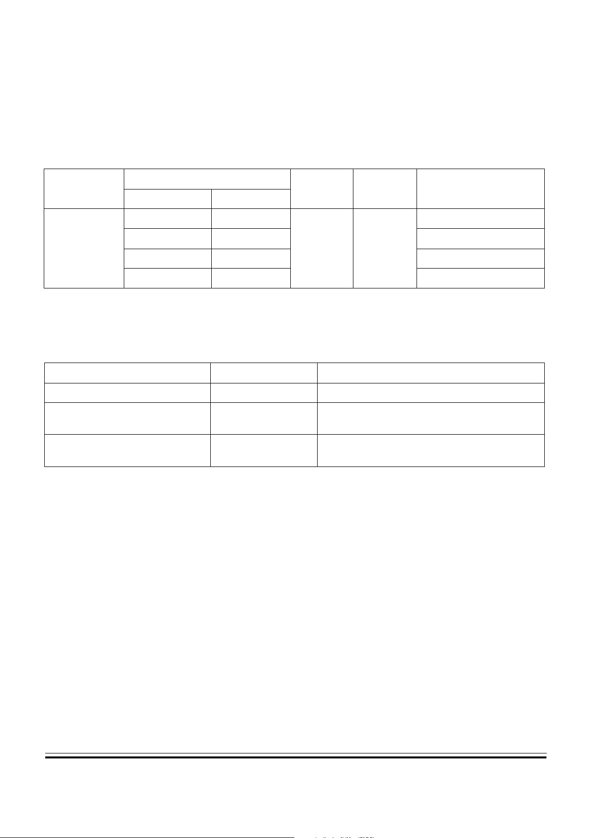
Table 1-1. Device Ordering Information
General Description
Ordering Information
Package
0 to +70
112-Pin TQFP
Single Tray
60 Pcs
nc...
I
* Important: M temperature operation is available only for single chip modes
–40 to +85
–40 to +105°C V 68HC91 2DG128VPV8
–40 to +125
Temperature
Voltage Frequency Order Number
Range Designator
°C
°C C 68HC912DG128CPV8
4.5V–5.5V 8 MHz
°C M* 68HC912DG128MPV8
Table 1-2. Development Tools Ordering Information
Description Name Order Numb er
MCUez Free from World Wide Web
Serial Debug Interface SDI
Evaluation board EVB
M68SDIL (3–5V), M68DIL12 (SDIL + MCUez +
SDBUG12)
M68EVB912DG128 (EVB only)
M68KIT912DG128 (EVB + SDIL12)
NOTE: SDBUG12 is a P & E Micro Product. It can be obtained from P & E from
their web site (http://www.pemicro.com) for approximately $100.
cale Semiconductor,
Third party tools: http://www.mcu.motsps.com/dev_tools/3rd/in dex .htm
68HC912DG128PV8
Frees
MC68HC912DG128 — Rev 3.0 Technical Data
MOTOROLA General Description 27
For More Information On This Product,
Go to: www.freescale.com
Freescale Semiconductor, Inc.
General Description
1.5 MC68HC912DG128 Block Diagram
nc...
I
cale Semiconductor,
Frees
VRH1
ATD1
VRL1
VDDA
VSSA
AN10
AN11
AN12
AN13
AN14
AN15
AN16
AN17
DDRT
DDRS
DDRP
DDRK
DDRIB
TxCAN0
RxCAN0
TxCAN1
RxCAN1
VDD ×2
VSS
PORT AD1
PT0
PT1
PT2
PT3
PT4
PT5
PORT T
PT6
PT7
PS0
PS1
PS2
PS3
PS4
PORT S
PS5
PS6
PS7
PP0
PP1
PP2
PP3
PORT P
PK0
PK1
PK2
PK3
PORT K
PK7
PIB7
PIB6
PIB5
PORTIB
PIB4
×2
Power for internal circuitry
VDDX ×2
×2
VSSX
Power for I/O drivers
VRH1
VRL1
VDDA
VSSA
PAD10
PAD11
PAD12
PAD13
PAD14
PAD15
PAD16
PAD17
PORT AD0
SDI/MISO
SDO/MOSI
IIC
DDRH
DDRJ
VRH0
VRL0
IOC0
IOC1
IOC2
IOC3
IOC4
IOC5
IOC6
IOC7
RxD0
TxD0
RxD1
TxD1
SCK
PW0
PW1
PW2
PW3
PIX0
PIX1
PIX2
I/O
ECS
SCL
SDA
PORTH
PORTJ
PAD00
PAD01
PAD02
PAD03
PAD04
PAD05
PAD06
PAD07
SS
I/O
PH7
PH6
PH5
PH4
PH3
PH2
PH1
PH0
PJ7
PJ6
PJ5
PJ4
PJ3
PJ2
PJ1
PJ0
VRH0
ATD0
VFP
VSTBY
BKGD
XFC
VDDPLL
VSSPLL
EXTAL
XTAL
RESET
128K byte flash EEPROM
8K byte RAM
2K byte EEPROM
CPU12
Single-wire
background
debug module
Clock
PLL
Generation
module
Periodic interrupt
COP watchdog
Clock monitor
Breakpoints
VDDA
VSSA
AN00
AN01
AN02
AN03
AN04
AN05
AN06
AN07
Enhanced
capture
timer
SCI0
SCI1
VRL0
SPI
PE0
PE1
PE2
PE3
PE4
PE5
PE6
PE7
XIRQ
IRQ
R/W
LSTRB
ECLK
MODA
PORT E
MODB
DBE/CAL
Lite
integration
module
(LIM)
PWM
PPAGE
Multiplexed Address/Data Bus
KWH7
KWH6
KWH5
KWH4
KWH3
KWH2
KWH1
KWH0
KWU
KWJ7
KWJ6
KWJ5
KWJ4
KWJ3
KWJ2
KWJ1
KWJ0
CAN0
CAN1
Wide
bus
DDRA
PORT A
PA4
PA7
PA6
PA5
5
4
3
2
1
1
1
1
R
R
R
R
D
D
D
D
D
D
D
D
A
A
A
A
DATA15
DATA14
DATA13
DATA12
DATA7
DATA6
DATA5
DATA4
Narrow bus
DDRB
PORT B
PB4
PB3
PB2
PB1
PB7
PB6
PA3
PA2
PA1
PA0
0
1
1
1
9
8
R
R
R
R
D
D
D
D
D
D
D
D
A
A
A
A
DATA11
DATA9
DATA8
DATA10
DATA3
DATA2
DATA1
DATA0
PB5
7
6
5
R
R
R
D
D
D
D
D
D
A
A
A
DATA7
DATA6
DATA5
PB0
4
3
2
1
0
R
R
R
R
R
D
D
D
D
D
D
D
D
D
D
A
A
A
A
A
DATA4
DATA3
DATA2
DATA1
DATA0
Technical Data MC68HC912DG128 — Rev 3.0
28 General Description MOTOROLA
For More Information On This Product,
Go to: www.freescale.com

Freescale Semiconductor, Inc.
Technical Data — MC68HC912DG128
Section 2. Central Processing Unit
2.1 Contents
2.2 Introduction. . . . . . . . . . . . . . . . . . . . . . . . . . . . . . . . . . . . . . . . 29
2.3 Programming Model. . . . . . . . . . . . . . . . . . . . . . . . . . . . . . . . .29
nc...
I
2.2 Introduction
cale Semiconductor,
Frees
2.4 Data Types. . . . . . . . . . . . . . . . . . . . . . . . . . . . . . . . . . . . . . . .31
2.5 Addressing Modes . . . . . . . . . . . . . . . . . . . . . . . . . . . . . . . . . .31
2.6 Indexed Addressing Modes . . . . . . . . . . . . . . . . . . . . . . . . . . .34
2.7 Opcodes and Operands . . . . . . . . . . . . . . . . . . . . . . . . . . . . . .35
The CPU12 is a hi gh-speed, 16-bit processing uni t. It has full 16-b it data
paths and wider internal registers (up to 20 bits) for high-speed extended
math instructions. The instruction set is a proper superset of the
M68HC11instruction set. The CPU12 allows instructions with odd byte
counts, including many single-byte instructions. This provides efficient
use of ROM space. An in struction queue buffers program informatio n so
the CPU always ha s immediate access to at least three bytes of machine
code at the start of every instruction. The CPU12 also offers an
extensive set of indexed addressing cap ab ilities.
2.3 Programming Model
CPU12 registers are a n inte gral pa rt of t he CPU a nd ar e not ad dressed
as if they were memory locations.
MC68HC912DG128 — Rev 3.0 Technical Data
MOTOROLA Central Processing Unit 29
For More Information On This Product,
Go to: www.freescale.com

Freescale Semiconductor, Inc.
Central Processing Unit
7
15
15
15
15
nc...
I
15
AB
70
D
IX
IY
SP
PC
NSXHI ZVC
0
8-BIT ACCUMULATORS A & B
OR
0
16-BIT DOUBLE ACCUMULATOR D
0
INDEX REGISTER X
0
INDEX REGISTER Y
0
STACK POINTER
0
PROGRAM COUNTER
CONDITION CODE REGISTER
Figure 2-1. Programming Model
Accumulators A and B are genera l-purpose 8-bit a ccumulators used to
hold operands and results of arithmetic calculations or data
manipulations. Some instructions treat the combination of these two 8bit accumulators as a 16-bit double accumulator (accumulator D).
Index registers X and Y are used for indexed addressing mode. In the
cale Semiconductor,
indexed addressing mode, the contents of a 16-bit index register are
added to 5-bit, 9-bit, or 16-bit constants or the content of an accumulator
to form the effective addr ess of the operand to be used in the i nstruction.
Frees
Stack pointer (SP) points to the last stack location used. The CPU12
supports an automatic program stack that is used to save system
context during su br ou tine calls and interrupts, and can also be u s ed fo r
temporary storage of data. The stack pointer can also be used in all
indexed addressing modes.
Program counter is a 16-bit register that holds the address of the next
instruction to be executed. The program counter can be used in all
indexed addr essing modes except autoinc rement/decrement.
Technical Data MC68HC912DG128 — Rev 3.0
30 Central Processing Unit MOTOROLA
For More Information On This Product,
Go to: www.freescale.com

nc...
I
2.4 Data Types
Freescale Semiconductor, Inc.
Condition Code Register (CCR) contains five status indicators, two
interrupt masking bits, and a STOP disable bit. The five flags are half
carry (H), negative (N), zero (Z), overflow (V), and carry/borrow (C). The
half-carry flag is use d only for BCD arithmetic operations. The N, Z, V,
and C status bits allow for branchin g based on the results of a pr evious
operation.
After a reset, the CPU fetches a vector from the appropriate address and
begins executing instructions. The X and I interrupt mask bits are set to
mask any interrupt requests. The S bit is also set to inhibit the STOP
instruction.
Central Processing Unit
Data Types
cale Semiconductor,
2.5 Addressing Modes
Frees
The CPU12 supports the following data types:
• Bit data
• 8-bit and 16-bit signed and unsigned integers
• 16-bit unsigned fractions
• 16-bit addresses
A byte is eight bits wide and can be accessed at any byte location. A
word is composed of two consecutive bytes with the most significant
byte at the lower value address. There are no special requirements for
alignment of instructions or operands.
Addressing modes determine how the CPU accesses memory locations
to be operated upon. The CPU12 includes all of the addressing modes
of the M68HC11 CPU as well as several new forms of indexed
addressing. Table 2-1 is a summary of the available addressing modes.
MC68HC912DG128 — Rev 3.0 Technical Data
MOTOROLA Central Processing Unit 31
For More Information On This Product,
Go to: www.freescale.com

Central Processing Unit
Addressing Mode Source Format Abbreviation Description
Inherent
Immediate
Direct INST opr8a DIR
Extended INST opr16a EXT Operand is a 16-bit address
Relative
nc...
I
Indexed
(5-bit offset)
Indexed
(auto pre-decrement)
Indexed
(auto pre-increment)
Indexed
(auto post-
decrement)
Indexed
(auto post-increment)
Indexed
(accumulator offset)
Indexed
(9-bit offset)
Indexed
(16-bit offset)
cale Semiconductor,
Indexed-Indirect
(16-bit offset)
Indexed-Indirect
Frees
(D accumulator
offset)
Freescale Semiconductor, Inc.
Table 2-1. M68HC12 A ddressing Mode Summary
INST
(no externally supplied
operands)
INST #opr8i
or
INST #opr16i
INST rel8
or
INST rel16
INST oprx5,xysp IDX 5-bit signed constant offset from x, y, sp, or pc
INST oprx3,–xys IDX Auto pre-decrement x, y, or sp by 1 ~ 8
INST oprx3,+xys IDX Auto pre-increment x, y, or sp by 1 ~ 8
INST oprx3,xys– IDX Auto post-decrement x, y, or sp by 1 ~ 8
INST oprx3,xys+ IDX Auto post-increment x, y, or sp by 1 ~ 8
INST abd,xysp IDX
INST oprx9,xysp IDX1
INST oprx16,xysp IDX2
INST [oprx16,xysp] [IDX2]
INST [D,xysp] [D,IDX]
INH Operands (if any) are in CPU registers
IMM
REL
Operand is included in instruction stream
8- or 16-bit size implied by context
Operand is the lower 8-bits of an address in the
range $0000 – $00FF
An 8-bit or 16-bit relative offset from the current
pc is supplied in the instruction
Indexed with 8-bit (A or B) or 16-bit (D)
accumulator offset from x, y, sp, or pc
9-bit signed constant offset from x, y, sp, or pc
(lower 8-bits of offset in one extension byte)
16-bit constant offset from x, y, sp, or pc
(16-bit offset in two extension bytes)
Pointer to operand is found at...
16-bit constant offset from x, y, sp, or pc
(16-bit offset in two extension bytes)
Pointer to operand is found at...
x, y, sp, or pc plus the value in D
Technical Data MC68HC912DG128 — Rev 3.0
32 Central Processing Unit MOTOROLA
For More Information On This Product,
Go to: www.freescale.com

Freescale Semiconductor, Inc.
Central Processing Unit
Table 2-2. M68HC12 A ddressing Mode Summary
Addressing Mode Source Format Abbreviation Description
INST
Inherent
(no externally
supplied operands)
INH Operands (if any) are in CPU registers
Addressing Modes
nc...
I
cale Semiconductor,
Frees
INST #opr8i
Immediate
Direct INST opr8a DIR
Extended INST opr16a EXT Operand is a 16-bit address
Relative
Indexed
(5-bit offset)
Indexed
(auto pre-decrement)
Indexed
(auto pre-increment)
Indexed
(auto post-decrement)
Indexed
(auto post-increment)
Indexed
(accumulator offset)
Indexed
(9-bit offset)
INST oprx5,xysp IDX
INST oprx3,–xys IDX Auto pre-decrement x, y, or sp by 1 ~ 8
INST oprx3,+xys IDX Auto pre-increment x, y, or sp by 1 ~ 8
INST oprx3,xys– IDX Auto post-decrement x, y, or sp by 1 ~ 8
INST oprx3,xys+ IDX Auto post-increment x, y, or sp by 1 ~ 8
INST oprx9,xysp IDX1
or
INST #opr16i
INST rel8
or
INST rel16
INST abd,xysp IDX
IMM
REL
Operand is included in instruction stream
8- or 16-bit size implied by context
Operand is the lower 8-bits of an address in
the range $0000 – $00FF
An 8-bit or 16-bit relative offset from the
current pc is supplied in the instruction
5-bit signed constant offset from x, y, sp, or
pc
Indexed with 8-bit (A or B) or 16-bit (D)
accumulator offset from x, y, sp, or pc
9-bit signed constant offset from x, y, sp, or
pc
(lower 8-bits of offset in one extension byte)
Indexed
(16-bit offset)
Indexed-Indirect
(16-bit offset)
Indexed-Indirect
(D accumulator offset)
MC68HC912DG128 — Rev 3.0 Technical Data
MOTOROLA Central Processing Unit 33
INST oprx16,xysp IDX2
INST [oprx16,xysp] [IDX2]
INST [D,xysp] [D,IDX]
For More Information On This Product,
Go to: www.freescale.com
16-bit constant offset from x, y, sp, or pc
(16-bit offset in two extension bytes)
Pointer to operand is found at...
16-bit constant offset from x, y, sp, or pc
(16-bit offset in two extension bytes)
Pointer to operand is found at...
x, y, sp, or pc plus the value in D

Freescale Semiconductor, Inc.
Central Processing Unit
2.6 Indexed Addressing Modes
The CPU12 indexed modes reduce execution time and eliminate code
size penalties fo r using the Y inde x register. CP U12 indexed ad dressing
uses a postbyte plus zero, one, or two extension bytes after the
instruction opcode. The postbyte and extension s do th e fo llowing ta sks:
• Specify which index register is used.
• Determine whethe r a value in an accumula tor is used as an offset.
• Enable automatic pre- or post-increment or decrement
• Specify use of 5-bit, 9-bit, or 16-bit signed offsets.
nc...
I
cale Semiconductor,
Frees
Table 2-3. Summary of Indexed Operations
Postbyte
Code (xb)
rr0nnnnn
111rr0zs
111rr011 [n,r]
rr1pnnnn
111rr1aa
Source
Code
Syntax
,r
n,r
–n,r
n,r
–n,r
n,–r n,+r
n,r– n,r+
A,r
B,r
D,r
Comments
5-bit constant offset n = –16 to +15
rr can specify X, Y, SP, or PC
Constant offset (9- or 16-bit signed)
z-0 = 9-bit with sign in LSB of postbyte(s)
1 = 16-bit
if z = s = 1, 16-bit offset indexed-indirect (see below)
rr can specify X, Y, SP, or PC
16-bit offset indexed-indirect
rr can specify X, Y, SP, or PC
Auto pre-decrement/incremen t or Auto post-
decrement/increment;
p = pre-(0) or post-(1), n = –8 to –1, +1 to +8
rr can specify X, Y, or SP (PC not a valid choice)
Accumulator offset (unsigned 8-bit or 16-bit)
aa-00 = A
01 = B
10 = D (16-bit)
11 = see accumulator D offset indexed-indirect
rr can specify X, Y, SP, or PC
111rr111 [D,r]
Technical Data MC68HC912DG128 — Rev 3.0
34 Central Processing Unit MOTOROLA
For More Information On This Product,
Accumulator D offset indexed-indirect
rr can specify X, Y, SP, or PC
Go to: www.freescale.com

Freescale Semiconductor, Inc.
2.7 Opcodes and Operands
The CPU12 uses 8-bit opcodes. Each opcode identifies a particular
instruction and associated addressing mode to the CPU. Several
opcodes are required to provide each instruction with a range of
addressing capabilities.
Only 256 opcodes would be available if the range of values were
restricted to the number that can be represented by 8-bit binary
numbers. To expand the num ber of opcodes, a second page i s added to
the opcode map. Opcodes on the second page are preceded by an
additional byte with the value $18.
Central Processing Unit
Opcodes and Operands
nc...
I
cale Semiconductor,
Frees
To provide additional addressing flexibility, opcodes can also be
followed by a postby te or ex tensio n by tes. Postb ytes impl eme nt cert ain
forms of indexed addr essing, transfers, e xchanges, and l oop primitiv es.
Extension bytes contain additional program information such as
addresses, offsets, and immedi at e data .
MC68HC912DG128 — Rev 3.0 Technical Data
MOTOROLA Central Processing Unit 35
For More Information On This Product,
Go to: www.freescale.com

Central Processing Unit
nc...
I
Freescale Semiconductor, Inc.
cale Semiconductor,
Frees
Technical Data MC68HC912DG128 — Rev 3.0
36 Central Processing Unit MOTOROLA
For More Information On This Product,
Go to: www.freescale.com

Freescale Semiconductor, Inc.
Technical Data — MC68HC912DG128
Section 3. Pinout and Signal Descriptions
3.1 Contents
3.2 Pin Assignments in 112-pin QFP . . . . . . . . . . . . . . . . . . . . . . .37
3.3 Power Supply Pins . . . . . . . . . . . . . . . . . . . . . . . . . . . . . . . . . .40
nc...
I
3.4 Signal Descriptions. . . . . . . . . . . . . . . . . . . . . . . . . . . . . . . . . .42
3.5 Port Signals . . . . . . . . . . . . . . . . . . . . . . . . . . . . . . . . . . . . . . .51
3.2 Pin Assignments in 112-pin QFP
The MC68HC912DG128 is available in a 112-pin thin quad flat pack
(TQFP). Most pins perform two or more functions, as described in the
Signal Descriptions. Figure 3-2 shows pin assignments. In expanded
narrow modes the lower byte data is multiplexed with higher byte data
through pins 57-64.
cale Semiconductor,
Frees
MC68HC912DG128 — Rev 3.0 Technical Data
MOTOROLA Pinout and Signal Descriptions 37
For More Information On This Product,
Go to: www.freescale.com

Freescale Semiconductor, Inc.
Pinout and Signal Descriptions
nc...
I
cale Semiconductor,
Frees
PP3/PW3
PK0/PIX0
PK1/PIX1
111
112
V
PK3
V
1
2
3
4
5
6
7
8
9
10
11
12
DD
13
14
SS
15
16
17
18
19
20
21
22
23
24
25
26
27
28
293031323334353637383940414243444546474849505152535455
ADDR5/DATA5/PB5
ADDR6/DATA6/PB6
ADDR7/DATA7/PB7
PW2/PP2
PW1/PP1
PW0/PP0
IOC0/PT0
IOC1/PT1
IOC2/PT2
IOC3/PT3
KWJ7/PJ7
KWJ6/PJ6
KWJ5/PJ5
KWJ4/PJ4
IOC4/PT4
IOC5/PT5
IOC6/PT6
SMODN/TAGHI/
IOC7/PT7
KWJ3/PJ3
KWJ2/PJ2
KWJ1/PJ1
KWJ0/PJ0
BKGD
ADDR0/DATA0/PB0
ADDR1/DATA1/PB1
ADDR2/DATA2/PB2
ADDR3/DATA3/PB3
ADDR4/DATA4/PB4
DDXVSSX
PK2/PIX2
PK7/ECS
V
RxCAN0
TxCAN0
RxCAN1
TxCAN1
PIB4
110
109
108
107
106
105
104
103
102
101
MC68HC912DG128
SSX
V
CAL/PE7
KWH7/PH7
KWH6/PH6
KWH5/PH5
KWH4/PH4
ECLK/PE4
DBE/
MODB/IPIPE1/PE6
MODA/IPIPE0/PE5
*
PIB5
100
VSTBY
FP
PIB6/SDA
PIB7/SCL
V
PS7/SS
PS6/SCK
PS5/SDO/MOSI
PS4/SDI/MISO
PS3/TxD1
PS2/RxD1
999897969594939291908988878685
112TQFP
DDX
XFC
V
DDPLL
V
XTAL
SSPLL
EXTAL
V
RESET
KWH3/PH3
KWH2/PH2
PS1/TxD0
KWH1/PH1
SSAVRL1VRH1VDDA
PS0/RxD0
V
KWH0/PH0
/TAGLO/PE3
LSTRB
/PE2
R/W
/PE1
IRQ
84
PAD17/AN17
83
PAD07/AN07
82
PAD16/AN16
81
PAD06/AN06
80
PAD15/AN15
79
PAD05/AN05
78
PAD14/AN14
77
PAD04/AN04
76
PAD13/AN13
75
PAD03/AN03
74
PAD12/AN12
73
PAD02/AN02
72
PAD11/AN11
71
PAD01/AN01
70
PAD10/AN10
69
PAD00/AN00
68
V
RL0
67
V
RH0
66
V
SS
65
V
DD
64
PA7/ADDR15/DATA15/DATA7
63
PA6/ADDR14/DATA14/DATA6
62
PA5/ADDR13/DATA13/DATA5
61
PA4/ADDR12/DATA12/DATA4
60
PA3/ADDR11/DATA11/DATA3
59
PA2/ADDR10/DATA10/DATA2
58
PA1/ADDR9/DATA9/DATA1
57
PA0/ADDR8/DATA8/DATA0
56
/PE0
XIRQ
Figure 3-1. MC68HC912DG128 Pin Assignments in 112-pin QFP
Technical Data MC68HC912DG128 — Rev 3.0
38 Pinout and Signal Descriptions MOTOROLA
For More Information On This Product,
Go to: www.freescale.com

Freescale Semiconductor, Inc.
Pin Assignments in 112-pin QFP
Pinout and Signal Descriptions
nc...
I
cale Semiconductor,
Frees
PIN 1
IDENT
C
4X
112 85
1
VIEW Y
L
28 57
29 56
C2
0.050
C1
VIEW AB
S1
A1
T
L-M0.20 N
4X 28 TIPS
N
A
S
2θ
3
θ
θ
R
R2
R1
R
(K)
E
(Y)
(Z)
L-M0.20 NT
84
V
B
M
B1
V1
VIEW AB
112X
T
0.10
SEATING
PLANE
T
0.25
GAGE PLANE
1θ
J1
J1
C
L
108X
J
0.13 NT
SECTION J1-J1
ROTATED 90 COUNTERCLOCKWISE
°
NOTES:
1. DIMENSIONING AND TOLERANCING PER
ASME Y14.5M, 1994.
2. DIMENSIONS IN MILLIMETERS.
3. DATUMS L, M AND N TO BE DETERMINED AT
SEATING PLANE, DATUM T.
4. DIMENSIONS S AND V TO BE DETERMINED AT
SEATING PLANE, DATUM T.
5. DIMENSIONS A AND B DO NOT INCLUDE
MOLD PROTRUSION. ALLOWABLE
PROTRUSION IS 0.25 PER SIDE. DIMENSIONS
A AND B INCLUDE MOLD MISMATCH.
6. DIMENSION D DOES NOT INCLUDE DAMBAR
PROTRUSION. ALLOWABLE DAMBAR
PROTRUSION SHALL NOT CAUSE THE D
DIMENSION TO EXCEED 0.46.
DIMAMIN MAX
A1 10.000 BSC
B 20.000 BSC
B1 10.000 BSC
C --- 1.600
C1 0.050 0.150
C2 1.350 1.450
D 0.270 0.370
E 0.450 0.750
F 0.270 0.330
G 0.650 BSC
J 0.090 0.170
K 0.500 REF
P 0.325 BSC
R1 0.100 0.200
R2 0.100 0.200
S 22.000 BSC
S1 11.000 BSC
V 22.000 BSC
V1 11.000 BSC
Y 0.250 REF
Z 1.000 REF
AA 0.090 0.160
θ
θ
1
θ
2
θ
3
G
VIEW Y
F
D
M
MILLIMETERS
20.000 BSC
0 °
3 °
11 °
11 °
4X
P
X
X=L, M OR N
AA
L-M
8 °
7 °
13 °
13 °
BASE
METAL
Figure 3-2. 112-pin QFP Mechanical Dimensions (case no. 987)
MC68HC912DG128 — Rev 3.0 Technical Data
MOTOROLA Pinout and Signal Descriptions 39
For More Information On This Product,
Go to: www.freescale.com

Freescale Semiconductor, Inc.
Pinout and Signal Descriptions
3.3 Power Supply Pins
Power and ground pins are described below and summarized in Table
3-1.
3.3.1 Internal Power (VDD) and Ground (VSS)
Power is supplied to the MCU through VDD and VSS. Because fast signal
transitions place high, short-duration current demands on the power
supply, use bypass capacitors with high-frequency characteristics and
place them as close to the MCU as possible. Bypass requirements
nc...
I
depend on how heavily the MCU pins are loaded.
3.3.2 External Power (V
3.3.3 V
DDA
, V
cale Semiconductor,
External power and ground for I/O drivers. Because fast signal
transitions place high, short-duration current demands on the power
supply, use bypass capacitors with high-frequency characteristics and
place them as close to the MCU as possible. Bypass requirements
depend on how heavily the MCU pins are loaded.
SSA
Provides operating volt age and gr ou nd for the ana l og-to-digital
converter. This allows the supply voltage to the ATD to be bypassed
independently. Connecting V
used will not result in an increase of power consumption.
and Ground (V
DDX)
Frees
3.3.4 Analog to Digital Reference Voltages (VRH, VRL)
V
RH0
, V
: reference voltage high and low for ATD converter 0.
RL0
SSX
)
to VDD if the ATD modules are not
DDA
V
, V
RH1
If the ATD modules are not use d, leavin g VRH connected to VDD will not
result in an increase of power consumption.
Technical Data MC68HC912DG128 — Rev 3.0
40 Pinout and Signal Descriptions MOTOROLA
For More Information On This Product,
: reference voltage high and low for ATD converter 1.
RL1
Go to: www.freescale.com

Freescale Semiconductor, Inc.
Pinout and Signal Descriptions
Power Supply Pins
nc...
I
cale Semiconductor,
Frees
3.3.5 V
DDPLL
3.3.6 XFC
, V
SSPLL
Provides operating voltage and ground for the P hase-Locked Loop. This
allows the supply voltage to the PLL to be bypassed independently.
NOTE: The VSSP LL pin should always be grou nded even if the PLL is not used.
The VDDPLL pin should not be left floating. It is recommended to
connect the VDDPLL pin to ground if the PLL is not used.
PLL loop filter. Please see Appendix: CGM Practical Aspects for
information on how to calculate PLL loop filter elements. Any current
leakage on this pin must be avoided.
VDDPLL
C
0
MCU
XFC
R
0
Figure 3-3. PLL Loop FIlter Connections
If VDDPLL is connected to VS S (t hi s is norm a l case ) , then the XFC pin
should either be left floating or connected to VSS (never to VDD). If
VDDPLL is tied to VD D but the PLL is switch ed off (PLLON bit cleare d),
then the XFC pin should be connected pre ferably t o VDDPLL ( i.e. read y
for VCO minimum frequency).
C
p
3.3.7 V
FP
Flash EEPROM program/erase voltage and supply voltage during
normal operation.
MC68HC912DG128 — Rev 3.0 Technical Data
MOTOROLA Pinout and Signal Descriptions 41
For More Information On This Product,
Go to: www.freescale.com

Freescale Semiconductor, Inc.
Pinout and Signal Descriptions
nc...
I
3.3.8 V
STBY
Mnemonic
V
DD
V
SS
V
DDX
V
SSX
V
DDA
V
SSA
V
RH1
V
RL1
V
RH0
V
RL0
V
DDPLL
V
SSPLL
V
FP
V
STBY
Pin Number
112-pin QFP
cale Semiconductor,
3.4 Signal Descriptions
Stand-by voltage supp ly to static RAM . Used to mainta in the contents of
RAM with minimal power when the rest of the chip is powered down.
Table 3-1. Power and Ground Connection Summary
Description
12, 65
14, 66
42, 107
40, 106
85
88
86
87
67
68
43
45
97
41
Internal power and ground.
External power and ground, supply to pin drivers.
Operating voltage and ground for the analog-to-digital converter, allows the
supply voltage to the A/D to be bypassed independently.
Reference voltages for the analog-to-digital converter 1
Reference voltages for the analog-to-digital converter 0.
Provides operating voltage and ground for the Phase-Locked Loop. This allows
the supply voltage to the PLL to be bypassed independently.
Program/erase voltage for the Flash EEPROM and required supply for normal
operation.
Stand-by voltage supply to maintain the contents of RAM with minimal power
when the rest of the chip is powered down.
Frees
3.4.1 Crystal Driver and External Clock Input (XTAL, EXTAL)
These pins provide the interface for either a crystal or a CMOS
compatible clock to control the internal clock generator circuitry. Out of
reset the frequency app lied to EXTAL is tw ice t he desir ed E–clock rate .
All the device clocks are derived from the EXTAL input frequency.
NOTE: CRYSTAL CIRCUIT IS CHANGED FROM STANDARD.
Technical Data MC68HC912DG128 — Rev 3.0
42 Pinout and Signal Descriptions MOTOROLA
For More Information On This Product,
Go to: www.freescale.com

Freescale Semiconductor, Inc.
Pinout and Signal Descriptions
Signal Descriptions
NOTE: The inte rnal return p ath for the osci llator is th e VSSPLL pin. Th erefore it
is recommended t o conne ct the co mmo n node of the reson ator and th e
capacitor d irectly to the VSSPLL pin.
2 x E crystal or ceramic resonator
EXTAL
nc...
I
cale Semiconductor,
Frees
MCU
XTAL
C1
C2
Figure 3-4. Common Crystal Connections
NOTE: When se lecting a cr ystal, it is r ecommended t o use one w ith the lo west
possible frequency in order to minimise EMC emissions.
2 x E
CMOS-COMPATIBLE
MCU
EXTAL
XTAL
NC
EXTERNAL OSCILLATOR
Figure 3-5. External Oscillator Connections
XTAL is the crystal output.Th e XTAL pin must be left untermina ted when
an external CMOS compatible clock input is connected to the EXTAL
pin. The XTAL output is normally intended to drive only a crystal. The
XTAL output can be buffered with a high-impedance buffer to drive the
EXTAL input of another device.
In all cases take extra care in the circuit board layout around the
oscillator pins. Load capacitances in the oscillator circuits include all
stray layout capacitances. Refer to Figure 3-4 and Figure 3-5 for
diagrams of oscillator circuits.
MC68HC912DG128 — Rev 3.0 Technical Data
MOTOROLA Pinout and Signal Descriptions 43
For More Information On This Product,
Go to: www.freescale.com

Pinout and Signal Descriptions
3.4.2 E-Clock Output (ECLK)
ECLK is the output connection for the internal bus clock. It is used to
demultiplex the address and data in expanded modes and is used as a
timing reference. ECLK frequency is equal to 1/2 the crystal frequency
out of reset. Th e E-clo ck output is tu rned off i n sing le ch ip user mo de to
reduce the effects of RFI. It can be turned on if necessary. In special
single-chip mode, the E-clock is turned ON at reset and can be turned
OFF. In special peripheral mode the E-clock is an input to the MCU. All
clocks, including the E clock, are halted when the MCU is in STOP
mode. It is possible to configure the MCU to interface to slow external
memory. ECLK can be stretched for such accesses.
nc...
I
Freescale Semiconductor, Inc.
3.4.3 Reset (RESET)
cale Semiconductor,
Frees
An active low bidirectional control signal, RESET, acts as an input to
initialize the MCU to a known start- up state. It also acts as an open-drain
output to indicate that an internal failure has been detected in either the
clock monitor or COP watchdog circuit. The MCU goes into reset
asynchronously and comes out of reset synch ro no usl y. This al low s the
part to reach a proper reset state even if the clocks have failed, while
allowing synchronized operation when starting out of reset.
It is important to use an external low-voltage reset circuit (such as
MC34064 or MC34164) to prevent corruption of RAM or EEPROM due
to power transitions.
The reset sequence is initiated by any of the following events:
• Power-on-reset (POR)
• COP watchdog enabled and watchdog timer times out
• Clock monitor enabled and C lock monitor detects slow or stopped
clock
• User applies a low level to the reset pin
External circuitry connected to the reset pin s hould not include a large
capacitance that would interfere with the ability of this signal to rise to a
valid logic one within nine bus cycles after the low drive is released.
Technical Data MC68HC912DG128 — Rev 3.0
44 Pinout and Signal Descriptions MOTOROLA
For More Information On This Product,
Go to: www.freescale.com

Freescale Semiconductor, Inc.
Upon detection of any reset, an internal circuit dr ives the reset pin low
and a clocked reset sequence controls when the MCU can begin normal
processing. In the case of POR or a clock monitor error, a 4096 cycle
oscillator startup delay is imposed before the reset recovery sequence
starts (reset is driven low throughout this 4096 cycle delay). The intern al
reset recovery sequence then drives reset low for 16 to 17 cycles and
releases the drive to allow reset to rise. Nine cycles later this circuit
samples the reset pin to see if it has rise n to a log ic on e level. If r eset is
low at this point, the reset is assumed to be coming from an external
request and the internally latched states of the COP time-out and clock
monitor failure are cleared so the normal reset vector ($FFFE:FFFF) is
taken when reset is finally released. If reset is high after this nine cycle
nc...
I
3.4.4 Maskable Interrupt Request (IRQ)
cale Semiconductor,
Frees
delay, the reset source is tentatively assumed to be either a COP failure
or a clock monitor fail. If the internally latched state of the clock monitor
fail circuit is true, processing begins by fetch ing the clock monitor vector
($FFFC:FFFD). If no clock monitor failure is indicated, and the latched
state of the COP tim e-out is true, processing beg ins by fetching the COP
vector ($FFFA:FFFB). If neither clock monitor fail nor COP time-out are
pending, processing begins by fetching the normal reset vector
($FFFE:FFFF).
The IRQ input provides a means of applying asynchronous interrupt
requests to the MCU. Either falling edge-sensitive triggering or levelsensitive triggering is program selectable (INTCR register). IRQ is
always enabled and configured to level-sensitive triggering at reset. It
can be disabled by clearing the IRQEN bit (INTCR register). When the
MCU is reset, the IRQ fun ction is masked in the con dition code regi ster.
Pinout and Signal Descriptions
Signal Descriptions
This pin is always an input and can always be read. There is an active
pull-up on this pi n while in reset and immediately out of reset. The pullup can be turned off by clearing PUPE in the PUCR register.
MC68HC912DG128 — Rev 3.0 Technical Data
MOTOROLA Pinout and Signal Descriptions 45
For More Information On This Product,
Go to: www.freescale.com

Freescale Semiconductor, Inc.
Pinout and Signal Descriptions
3.4.5 Nonmaskable Interrupt (XIRQ)
The XIRQ input provides a means of requesting a nonmaskable interrupt
after reset initialization. During reset, the X bit in the condition code
register (CCR) is set and any interrupt is masked until MCU software
enables it. Because the XIRQ input is level sensitive, it can be connected
to a multiple-source wired-OR network. This pin is always an input and
can always be read. There is an active pull-up on this pin while in reset
and immediately out of reset. The pull-up can be turned off by clearing
PUPE in the PUCR register. XIRQ is often used as a power loss detect
interrupt.
nc...
I
3.4.6 Mode Select (SMODN, MODA, and MODB)
cale Semiconductor,
Frees
Whenever XIRQ or IRQ are used with mul tiple interrupt sources (IRQ
must be configured for l evel-sensitive operat ion if there is more than o ne
source of IRQ interrupt), each source must drive the interrupt input with
an open-drain type of driver t o avoid con tention betw een outputs. There
must also be an interlock mechanism at each interrupt source so that the
source holds th e interrupt line low until the MCU recognizes and
acknowledges the interrupt request. If the interrupt line is held low, the
MCU will recognize another interrupt as soon as the interrupt mask bit in
the MCU is cleared (normally upon return from an interrupt).
The state of these pins during reset determine the MCU operating mode.
After reset, MODA and MODB can be configured as instruction queue
tracking signals IPIPE0 and IPIPE1 in expanded modes. MODA and
MODB have active pull-downs during reset.
The SMODN pin has an active pull-up when configured as an input. This
pin can be use d as BKGD or TAGHI after reset.
3.4.7 Single-Wire Background Mode Pin (BKGD)
The BKGD pin receives and transmits serial background debugging
commands. A sp ecial self -timing pr otocol is u sed. The BK GD pin has a n
active pull-up wh en configured as an input ; BKGD has no pull-up con trol.
Refer to Development Support.
Technical Data MC68HC912DG128 — Rev 3.0
46 Pinout and Signal Descriptions MOTOROLA
For More Information On This Product,
Go to: www.freescale.com

Freescale Semiconductor, Inc.
3.4.8 External Address and Data Buses (A DDR[15:0] and DATA[15:0])
External bus pins share functions with gener a l-pu r po se I/ O po r ts A and
B. In single-chip operating modes, the pins can be used for I/O; in
expanded modes, the pins are used for the external buses.
In expanded wide mode, ports A and B are used for multiplexed 16-bit
data and address buses. PA[7:0] correspond to
ADDR[15:8]/DATA[15:8]; PB[7:0] correspond to ADDR[7:0]/DATA[7:0].
In expanded narrow mode, ports A and B are used for the16 -bit address
bus, and an 8-bit data bus is multiplexed with the most significant half of
the address bus on port A. In this mode, 16-bit data is handled as two
nc...
I
back-to-back bus cycles, one for the high byte followed by one for the
low byte. PA[7:0] correspond to ADDR[15:8] and to DATA[15:8] or
DATA[7:0], depending on the bus cycle. The state of the address pins
should be latched at the r ising edge of E. To allow for m aximum address
setup time at ext ernal devices, a transparent latch should be used.
Pinout and Signal Descriptions
Signal Descriptions
3.4.9 Read/Write (R/W)
cale Semiconductor,
3.4.10 Low-Byte Strobe (LSTRB)
Frees
In all modes this pin can be used as a general-purpose I/O and is an
input with an active pull-up out of reset. If the read/write function is
required it should be enabled by setting the RDWE bit in the PEAR
register. External writes will not be possible until enabled.
In all modes this pin can be used as a general-purpose I/O and is an
input with an active p ull-up out of rese t. If the strobe fun ction is required ,
it should be enabl ed by setting th e LSTRE bit in t he PEAR re gister. This
signal is used in write operations and so external low byte writes will not
be possible until this fun ction is enabled. This pi n is also used as T AGLO
in Special Expanded modes and is multiplexed with the LSTRB function.
MC68HC912DG128 — Rev 3.0 Technical Data
MOTOROLA Pinout and Signal Descriptions 47
For More Information On This Product,
Go to: www.freescale.com

Freescale Semiconductor, Inc.
Pinout and Signal Descriptions
3.4.11 Instruction Queue Tracking Signals (IPIPE1 and IPIPE0)
These signals are used to track the state of the internal instruction
execution queue . Execution state i s time-multipl exed on the two sig nals.
Refer to Development Support.
3.4.12 Data Bus Enable (DBE)
The DBE pin (PE7) is an active low signal that will be asserted low during
E-clock high time. DBE provides separation between output of a
multiplexed addre ss and the input of da ta. When an exte rnal addr ess is
stretched, DBE is asserted during what would be the last quarter cycle
nc...
I
of the last E-clock cycle of stretch. In expanded modes this pin is used
to enable the dr i ve control of exte rn al buse s d ur i ng e xter n al r e ads. Use
of the DBE is controlled by the NDBE bit in the PEAR register. DBE is
enabled out of re set in expanded modes. This pi n h as an act ive pu ll- u p
during and after reset in single chip modes.
3.4.13 Inverted E clock (ECLK)
The ECLK pin (PE7) can be used to latch the address for demultiplexing. It has th e sam e behavior as the ECLK, except is inver te d.
In expanded modes this pin i s used to enable the drive control of external
buses during external reads. Use of the ECLK is controlled by the NDBE
and DBENE bits in the PEAR register.
cale Semiconductor,
3.4.14 Calibration reference (CAL)
Frees
The CAL pin (PE7) is the out put of the Slow Mode program mable clock
divider, SLWCLK, and is used as a cal ibra tion re fere nce. The SLWC LK
frequency is equal to the crystal frequency out of reset and always has
a 50% duty. If the DBE function is enabled it will override the enabled
CAL output. The CAL pin output is disabled by clearing CALE bit in the
PEAR register.
Technical Data MC68HC912DG128 — Rev 3.0
48 Pinout and Signal Descriptions MOTOROLA
For More Information On This Product,
Go to: www.freescale.com

Freescale Semiconductor, Inc.
3.4.15 Clock generation module test (CGMTST)
The CGMTST pin (PE6) is the ou tput of the clocks tested when CG MTE
bit is set in PEAR register. The PIPOE bit must be cleared for the clocks
to be tested.
Table 3-2. Signal Description Summary
Pinout and Signal Descriptions
Signal Descriptions
nc...
I
cale Semiconductor,
Frees
Pin Name
EXTAL - 47
XTAL - 48
RESET - 46
ADDR[7:0]
DATA[7:0]
ADDR[15:8]
DATA[15:8]
DBE PE7 36
ECLK PE7 36 Inverted E clock used to latch the address.
CAL PE7 36
CGMTST PE6 37 Clock gen erati on modu le tes t output .
MODB/
IPIPE1,
MODA/
IPIPE0
ECLK PE4 39
LSTRB/
TAGLO
R/W
IRQ PE1 55
Shared
port
PB[7:0] 31–24
PA[7:0] 64–57
PE6, PE5 37, 38
PE3 53
PE2 54
Pin
Number
112-pin
Description
Crystal driver and external clock input pins. On reset all the device clocks
are derived from the EXTAL input frequency. XTAL is the crystal output.
An active low bidirectional control signal, RESET
initialize the MCU to a known start-up state, and an output when COP or
clock monitor causes a reset.
External bus pins share function with general-purpose I/O ports A and B.
In single chip modes, the pins can be used for I/O. In expanded modes,
the pins are used for the external buses.
Data bus control and, in expanded mode, enables the drive control of
external buses during external reads.
CAL is the output of the Slow Mode programmable clock divider,
SLWCLK, and is used as a calibration reference for functions such as
time of day. It is overridden when DBE
a 50% duty.
State of mode select pins during reset determine the initial operating
mode of the MCU. After reset, MODB and MODA can be configured as
instruction queue tracking signals IPIPE1 and IPIPE0 or as generalpurpose I/O pins.
E Clock is the output connection for the external bus clock. ECLK is used
as a timing reference and for address demultiplexing.
Low byte strobe (0 = low byte valid), in all modes this pin can be used as
I/O. The low strobe function is the exclusive-NOR of A0 and the internal
signal. (The SZ8 internal signal indicates the size 16/8 access.) Pin
SZ8
function TAGLO
Indicates direction of data on expansion bus. Shares function with
general-purpose I/O. Read/write in expanded modes.
Maskable interrupt request input provides a means of applying
asynchronous interrupt requests to the MCU. Either falling edgesensitive triggering or level-sensitive triggering is program selectable
(INTCR register).
used in instruction tagging. See Development Support.
acts as an input to
function is enabled. It always has
MC68HC912DG128 — Rev 3.0 Technical Data
MOTOROLA Pinout and Signal Descriptions 49
For More Information On This Product,
Go to: www.freescale.com

Freescale Semiconductor, Inc.
Pinout and Signal Descriptions
Table 3-2. Signal Description Summary
nc...
I
cale Semiconductor,
Frees
Pin Name
XIRQ PE0 56
SMODN/
BKGD/
TAGHI
IX[2:0] PK[2:0] 109-111 Page Index register emulation outputs.
ECS PK7 108 Emulation Chip select.
PW[3:0] PP[3:0] 112, 1–3 Pulse Width Modulator channel outputs.
SS PS7 96
SCK PS6 95 Serial clock for SPI system.
SDO/MOSI PS5 94 Master out/slave in pin for serial peripheral interface
SDI/MISO PS4 93 Master in/slave out pin for serial peripheral interface
TxD1 PS3 9 2 SCI1 trans mit pin
RxD1 PS2 91 SCI1 receive pin
TxD0 PS1 9 0 SCI0 trans mit pin
RxD0 PS0 89 SCI0 receive pin
IOC[7:0] PT[7:0] 18–15, 7–4
AN1[7:0] PAD1[7:0]
AN0[7:0] PAD0[7:0]
TxCAN1 - 102 MSCAN1 transmit pin
RxCAN1 - 103 MSCAN1 receive pin
TxCAN0 - 104 MSCAN0 transmit pin
RxCAN0 - 105 MSCAN0 receive pin
SCL PIB7 98
SDA PIB6 99
KWJ[7:0] PJ[7:0]
KWH[7:0] PH[7:0]
Shared
port
-23
Pin
Number
112-pin
Provides a means of requesting asynchronous nonmaskable interrupt
requests after reset initialization
During reset, this pin determines special or normal operating mode. After
reset, single-wire background interface pin is dedicated to the
background debug function. Pin function TAGHI
tagging. See Development Support.
Slave sele ct output for SPI master mode, input for sl ave mode or master
mode.
Pins used for input capture and output compare in the timer and pulse
accumulator subsystem.
84/82/80/7
8/76/74/72/70Analog inputs for the analog-to-digital conversion module 1
83/81/79/7
7/75/73/71/69Analog inputs for the analog-to-digital conversion module 0
2
I
C bus serial clock line pin
2
I
C bus serial data line pin
8–11,
19–22
32–35,
49–52
Key wake-up and general purpose I/O; can cause an interrupt when an
input transitions from high to low or from low to high (KWPJ).
Key wake-up and general purpose I/O; can cause an interrupt when an
input transitions from high to low or from low to high (KWPH).
Description
used in instruction
Technical Data MC68HC912DG128 — Rev 3.0
50 Pinout and Signal Descriptions MOTOROLA
For More Information On This Product,
Go to: www.freescale.com

3.5 Port Signals
3.5.1 Port A
nc...
I
Freescale Semiconductor, Inc.
The MC68HC912D G128 incorporates eleven ports which are used to
control and access the various device subsystems. When not used for
these purposes, port pins may be used for general-purpose I/O. In
addition to the pins described below, each port consists of a data register
which can be read and writt en at any time, and, with the exception of po rt
AD0, port AD1, PE[1:0], RxCAN and TxCAN, a data direction register
which controls the direction of each pin. After reset all general purpose
I/O pins are configured as input.
Port A pins are u sed for add ress and data i n expanded modes. In sing le
chip modes, the pins can be used as gene ral purpose I/O. The port data
register is not in the address map during expanded and peripheral mode
operation. When it is in the ma p, port A can be r ead or written at anytime.
Pinout and Signal Descriptions
Port Signals
cale Semiconductor,
Frees
3.5.2 Port B
Register DDRA deter mines whether each port A pi n is an input or output.
DDRA is not in the address map during expanded and peripheral mode
operation. Setting a bit in DDRA makes the corresponding bit in port A
an output; clearing a bit in DDRA makes the corresponding bit in port A
an input. The default reset state of DDRA is all zeros.
When the PUPA bit in the PUCR re giste r is set, all por t A input pi ns are
pulled-up internally by an active pull-up device. PUCR is not in the
address map in peripheral mode.
Setting the RDPA bit in register RDRIV causes all port A outputs to have
reduced drive level. RDRIV can be writ ten once after reset. RDRIV is not
in the address map in peripheral mode. Refer to Bus Control and
Input/Output.
Port B pins are u sed for add ress and data i n expanded modes. In sing le
chip modes, the pins can be used as gene ral purpose I/O. The port data
register is not in the address map during expanded and peripheral mode
operation. When it is in the ma p, port B can be r ead or written at anytime.
MC68HC912DG128 — Rev 3.0 Technical Data
MOTOROLA Pinout and Signal Descriptions 51
For More Information On This Product,
Go to: www.freescale.com

Pinout and Signal Descriptions
Register DDRB deter mines whether each port B pi n is an input or output.
DDRB is not in the address map during expanded and peripheral mode
operation. Setting a bit in DDRB makes the corresponding bit in port B
an output; clearing a bit in DDRB makes the corresponding bit in port B
an input. The default reset state of DDRB is all zeros.
When the PUPB bit in the PUCR re giste r is set, all por t B input pi ns are
pulled-up internally by an active pull-up device. PUCR is not in the
address map in peripheral mode.
Setting the RDPB bit in register RDRIV causes all port B outputs to have
reduced drive level. RDRIV can be writ ten once after reset. RDRIV is not
nc...
I
in the address map in peripheral mode. Refer to Bus Control and
Input/Output.
Freescale Semiconductor, Inc.
3.5.3 Port E
cale Semiconductor,
Frees
Port E pins operate differently from port A and B pins. Port E pins are
used for bus contro l signals and interrup t service re quest signa ls. When
a pin is not used for one of these specific functions, it can be used as
general-purpose I/O. However, two of the pins (PE[1:0]) can only be
used for input, and t he states of these pins can be r ead i n th e po r t da ta
register even when they are used for IRQ and XIRQ.
The PEAR registe r determines pin function, and register DDRE
determines whether each pin is an input or output when it is used for
general-purpose I/O. PEAR settings override DDRE settings. Because
PE[1:0] are input-only pins, only DDRE[7:2] have effect. Setting a bit in
the DDRE register makes the corresponding bit in port E an output;
clearing a bit in the DDRE register makes the corresponding bit in port E
an input. The default reset state of DDRE is all zeros.
When the PUPE bit in the PUCR register is set, PE[7,3,2,1, 0] are pulled
up. PE[7,3,2,0] are active pull-up device s. PUPCR is not in t he add ress
map in peripheral mode.
Neither port E nor DDRE is in the map in peripheral mode; neither is in
the internal map in expanded modes with EME set.
Technical Data MC68HC912DG128 — Rev 3.0
52 Pinout and Signal Descriptions MOTOROLA
For More Information On This Product,
Go to: www.freescale.com

3.5.4 Port H
nc...
I
Freescale Semiconductor, Inc.
Setting the RDPE bit in register RDRIV causes all port E outputs to have
reduced drive level. RDRIV can be writ ten once after reset. RDRIV is not
in the address map in peripheral mode. Refer to Bus Control and
Input/Output.
Port H pins are used for key wake-ups that ca n be used with the pins
configured as inputs or outputs. The key wake-ups are triggered with
either a rising or fal ling edge sign al (KWPH ). An interrup t is genera ted if
the corresponding bit is en abl e d (K WI EH ). If any of the i nte rr u pts i s not
enabled, the corresponding pin can be used as a general purpose I/O
pin. Refer to I/O Ports with Key Wake-up.
Pinout and Signal Descriptions
Port Signals
cale Semiconductor,
Frees
Register DDRH determi nes whether each port H pin is an input or ou tput.
Setting a bit in DDRH makes the corresponding bit in port H an output;
clearing a bit in DDRH makes the correspondin g b it in port H a n in put.
The default reset state of DDRH is all zeros.
Register KWPH not only deter mines what type of edge the key wake ups
are triggered, but it also determines what type of resistive load is used
for port H input pins w hen P UPH bi t is set i n the P UCR reg ister. S etting
a bit in KWPH makes the corres ponding key wake up in put pin trigger at
rising edges and load s a pull down in the corr esponding port H input pin.
Clearing a bit in KW PH makes th e correspon ding key w ake up inpu t pin
trigger at falling edges and loads a pull up in the corresponding port H
input pin. The default state of KWPH is all zeros.
Setting the RDPH bit in register RDRIV causes all port H outputs to have
reduced drive level. RDRIV can be writ ten once after reset. RDRIV is not
in the address map in peripheral mode. Refer to Bus Control and
Input/Output.
3.5.5 Port J
Port J pins are used for key wake-ups that can be used with the pins
configured as inputs or outputs. The key wake-ups are triggered with
either a rising or falling e dge si gnal ( KWPJ). An i nterr upt is g enerate d if
MC68HC912DG128 — Rev 3.0 Technical Data
MOTOROLA Pinout and Signal Descriptions 53
For More Information On This Product,
Go to: www.freescale.com

Pinout and Signal Descriptions
the corresponding bit is enabled (KWIEJ). If any of the interrupts is not
enabled, the corresponding pin can be used as a general purpose I/O
pin. Refer to I/O Ports with Key Wake-up.
Register DDRJ determines whether each port J pin is an input or output.
Setting a bit in DDRJ makes the corresponding bit in port J an output ;
clearing a bit in DDRJ makes the corresponding bit in port J an input. The
default reset state of DDRJ is all zeros.
Register KWPJ not only determines what type of edge the key wake ups
are triggered, but it also determines what type of resistive load is used
for port J input pins whe n PUPJ bit is set in the PUCR registe r. Setting a
nc...
I
bit in KWPJ makes the corresponding key wake up input pin trigger at
rising edges and l oads a pull down in the co rrespondin g port J in put pin.
Clearing a bit in KWPJ makes the cor respo ndin g key wake up input pin
trigger at falling edges and loads a pull up in the corresponding port J
input pin. The default state of KWPJ is all zeros.
Freescale Semiconductor, Inc.
3.5.6 Port K
cale Semiconductor,
Frees
Setting the RDPJ bit in register RDRIV causes all port J outputs to have
reduced drive level. RDRIV can be writ ten once after reset. RDRIV is not
in the address map in peripheral mode. Refer to Bus Control and
Input/Output.
Port K pins are used for page index emulat ion in expa nded or perip heral
modes. When page index emulation is not enabled, EMK is not set in
MODE register, or the p art is in single chip mode , these pins can be used
for general purpose I/O. Port K bit 3 is used as a gene ral purpose I/O pin
only. The port data register is not in the address map during expanded
and peripheral mode operat ion with EM K set. When it is in the map, p ort
K can be read or written at anytime.
Register DDRK deter mines whether each port K pi n is an input or output.
DDRK is not in the address map during expanded and peripheral mode
operation with EMK set. Setting a bit in DDRK makes the corresponding
bit in port K an output; clearing a bit in DDRK makes the corresponding
bit in port K an input. The default reset state of DDRK is all zeros.
Technical Data MC68HC912DG128 — Rev 3.0
54 Pinout and Signal Descriptions MOTOROLA
For More Information On This Product,
Go to: www.freescale.com

3.5.7 Port CAN1
nc...
I
Freescale Semiconductor, Inc.
When the PUPK bit in the PUCR re giste r is set, all por t K input pi ns are
pulled-up internally by an active pull-up device. PUCR is not in the
address map in peripheral mode.
Setting the RDPK bit in register RDRIV causes all port K outputs to have
reduced drive level. RDRIV can be writ ten once after reset. RDRIV is not
in the address map in peripheral mode. Refer to Bus Control and
Input/Output.
The MSCAN1 uses two external pins, one input (RxCAN1) and one
output (TxCAN1). The TxCAN1 output pin represents the logic level on
the CAN: ‘0’ is for a dominant state, and ‘1’ is for a recessive state.
RxCAN1 is on bit 0 of Port CAN1, TxCAN1 is on bit 1.
Pinout and Signal Descriptions
Port Signals
3.5.8 Port CAN0
3.5.9 Port IB
cale Semiconductor,
Frees
The MSCAN0 uses two external pins, one input (RxCAN0) and one
output (TxCAN0). The TxCAN0 output pin represents the logic level on
the CAN: ‘0’ is for a dominant state, and ‘1’ is for a recessive state.
RxCAN0 is on bit 0 of Port CAN0, TxCAN0 is on bit 1.
Bidirectional pins to IIC bus interface subsystem. The IIC bus interface
uses a Serial Data line (SDA) and Serial Clock line (SCL) for data
transfer. The pins are connected to a positive voltage supply via a pull
up resistor. The pull ups can be enabled internally or connected
externally. The output stages have open drain outputs in order to
perform the wired-AND function. When the IIC is disabled the pins can
be used as gener al purpose I/O pins. SCL is on bit 7 of Port IB and S DA
is on bit 6. The remaining pins of Port IB (PIB[5:4]) are controlled by
registers in the IIC address space.
Register DDRIB determines pin direction of port IB when used for
general-purpose I/O. When DDRI B bits are set, the corresp onding pin is
MC68HC912DG128 — Rev 3.0 Technical Data
MOTOROLA Pinout and Signal Descriptions 55
For More Information On This Product,
Go to: www.freescale.com

Pinout and Signal Descriptions
configured for output. On reset the DDRIB bits are cleared and the
corresponding pin is configured for input.
When the PUPIB bit in the IBPURD register is set, all input pins are
pulled up internally by an active pull-up device. Pull-ups are disabled
after reset, except for input ports 0 through 3, which are always on
regardless of PUPIB bit.
Setting the RDPIB bit in the IBPURD register configures all port IB
outputs to have reduced drive levels. Levels are at normal drive
capability after reset. The IBPURD register can b e re ad or written
anytime after reset. Refer to section Inter-IC Bus.
nc...
I
3.5.10 Port AD1
Freescale Semiconductor, Inc.
3.5.11 Port AD0
cale Semiconductor,
Frees
This port is an analog inpu t in terfa c e to the a na log-to -di gita l subsystem
and used for general-purpose input. When analog-to-digital functions
are not enabled, the port has eight general-purpose input pins,
PAD1[7:0]. The ADPU bit in the ATD1CTL2 register enables the A/D
function.
Port AD1 pins are inpu ts; no data direction register is associ ated with this
port. The port has no resistive input loads and no reduced drive controls.
Refer to MSCAN Controller.
This port is an analog input interface to the analog-to-digital subsystem
and used for general-purpose input. When analog-to-digital functions are
not enabled, the port has eight general-purpose input pins, PAD0[7:0].
The ADPU bit in the ATD0CTL2 register enables the A/ D function.
Port AD0 pins are inpu ts; no data direction register is associ ated with this
port. The port has no resistive input loads and no reduced drive controls.
Refer to MSCAN Controller.
Technical Data MC68HC912DG128 — Rev 3.0
56 Pinout and Signal Descriptions MOTOROLA
For More Information On This Product,
Go to: www.freescale.com

3.5.12 Port P
Freescale Semiconductor, Inc.
The four pulse-widt h modulation channel outputs share gen eral-purpose
port P pins. The PWM function is enabled with the PWEN register.
Enabling PWM pins takes precedence over the general-purpose port.
When pulse-width modulation is not in use, the port pins may be used for
general-purpose I/O.
Register DDRP determines pin direction of port P when used for
general-purpose I/O. When DDRP bits are set, the corresponding pin is
configured for output. On reset the DDRP bi ts are cleared and the
corresponding pin is configured for input.
Pinout and Signal Descriptions
Port Signals
nc...
I
3.5.13 Port S
cale Semiconductor,
Frees
When the PUPP bit in the PWCTL register is set, all input pins are pulled
up internally by an active pull-up device. Pull-ups are disabled after reset.
Setting the RDPP bit in the PWCTL register configures all port P outputs
to have reduced drive levels. Levels are at normal drive capability after
reset. The PWCTL register can be read or written anytime after reset.
Refer to Pulse Width Modulator.
Port S is the 8-bit inte r face to the standard serial inte r face con s ist ing o f
the two serial com munications interf aces (SCI1 and SC I0) and the seri al
peripheral interface (SPI) subsystems. Port S pins are available for
general-purpose I/O when standard serial function s are not enab led.
Port S pins serve several functions depending on the various internal
control registers. If WOMS bit in the SC0CR1register is set, the Pchannel drivers of the ou tput buffers are disabled (wi re-or mode) for pins
0 through 3. If SWOM bit in the SP0CR1 register is set, the P-channel
drivers of the output buffers are disabled (wire-or mode) for pins 4
through 7. The open drai n control affects both the serial an d the generalpurpose outputs. If the RDPS bit in the SP0CR2 register is set, Port S
pin drive capabilities are reduced. If PUPS bit in the SP0CR2 register is
set, a pull-up device is activated for each port S pin programmed as a
general purpose input. If the pin is programmed as a general-purpose
output, the pull-u p is disconnected fr om the pin regardless of the state of
PUPS bit. See Multiple Serial Interface.
MC68HC912DG128 — Rev 3.0 Technical Data
MOTOROLA Pinout and Signal Descriptions 57
For More Information On This Product,
Go to: www.freescale.com

Freescale Semiconductor, Inc.
Pinout and Signal Descriptions
3.5.14 Port T
This port provides eight general-purpose I/O pin s when n ot en ab led fo r
input capture and output compare in the timer and pulse accumulator
subsystem. The TEN bit in the TSCR register enables the timer function.
The pulse accumulator subsystem is enabled with the PAEN bit in the
PACTL register.
Register DDRT determines pin direction of port T when used for generalpurpose I/O. When DDRT bits are set, the corresponding pin is
configured for output. On reset the DDRT bits are cleared and the
corresponding pin is configured for input.
nc...
I
cale Semiconductor,
Frees
When the PUPT bit in the TMSK 2 register is set, all in put pins are pulled
up internally by an active pull-up device. Pull- ups are disabled after
reset.
Setting the RDPT bit in the TMSK2 registe r configures all port T outputs
to have reduced drive levels. Levels are at normal drive capability after
reset. The TMSK2 register can be read or written anytime after reset
Refer to Enhanced Capture Timer.
Technical Data MC68HC912DG128 — Rev 3.0
58 Pinout and Signal Descriptions MOTOROLA
For More Information On This Product,
Go to: www.freescale.com

nc...
I
cale Semiconductor,
Frees
Port Name
Port A
PA[7:0]
Port B
PB[7:0]
Port AD1
PAD1[7:0]
Port AD0
PAD0[7:0]
Port CAN1
PCAN1[1:0]
Port CAN0
PCAN0[1:0]
Port IB
PIB[7:4]
Port IB
PIB[3:2]
Port E
PE[7:0]
Port K
PK[7,3:0]
Port P
PP[3:0]
Port S
PS[7:0]
Port T
PT[7:0]
Freescale Semiconductor, Inc.
Table 3-3. Port Description Summary
Pin Numbers Data Direction
112-pin
64-57
31–24
84/82/80/78/7
6/74/72/70
83/81/79/77/7
5/73/71/69
102–103
104–105
98–101
102–103
36–39, 53–56
13,
108-111
112,
1–3
96–89
18–15, 7–4
Register
(Address)
In/Out
DDRA ($0002)
In/Out
DDRB ($0003)
In Analog-to-digital converter 1 and general-purpose I/O.
In Analog-to-digital converter 0 and general-purpose I/O.
PCAN1[1] Out
PCAN1[0] In
PCAN0[1] Out
PCAN0[0] In
In/Out
DDRIB ($00E7)
In/Out
DDRIB ($00E7)
PE[1:0] In
PE[7:2] In/Out
DDRE ($0009)
In/Out
DDRK ($00FD)
In/Out
DDRP ($0057)
In/Out
DDRS ($00D7)
In/Out
DDRT ($00AF)
Pinout and Signal Descriptions
Port Signals
Description
Port A and port B pins are used for address and data in
expanded modes. The port data registers are not in the
address map during expanded and peripheral mode
operation. When in the map, port A and port B can be
read or written any time.
DDRA and DDRB are not in the address map in expanded
or peripheral modes.
PCAN1[1:0] are used with the MSCAN1 module and
cannot be used as general purpose I/O.
PCAN0[1:0] are used with the MSCAN0 module and
cannot be used as general purpose I/O.
General purpose I/O. PIB[7:6] are used with the I-Bus
module when enabled.
General purpose I/O
Mode selection, bus control signals and interrupt service
request signals; or general-purpose I/O.
Page index emulation signals in expanded or peripheral
mode or general-purpose I/O.
General-purpose I/O. PP[3:0] are used with the pulse-width
modulator when enabled.
Serial communications interfaces 1 and 0 and serial
peripheral interface subsystems; or general-purpose I/O.
General-purpose I/O when not enabled for input capture
and output compare in the timer and pulse accumulator
subsystem.
MC68HC912DG128 — Rev 3.0 Technical Data
MOTOROLA Pinout and Signal Descriptions 59
For More Information On This Product,
Go to: www.freescale.com

Freescale Semiconductor, Inc.
Pinout and Signal Descriptions
3.5.15 Port Pull-Up Pull-Down and Reduced Drive
MCU ports can be configured for internal pull-up. To reduce power
consumption a nd RFI, the pin output drivers ca n be configured to
operate at a r educed drive level . Reduced driv e causes a slight increase
in transition time depen ding on loading and should be use d only for ports
which have a light loading. Table 3-4 summarizes t he port pull-up/pulldown default status and controls.
Table 3-4. Port Pull-Up, Pull-Down and Reduced Drive Summary
Enable Bit Reduced Drive Control Bit
nc...
I
cale Semiconductor,
Frees
Port
Name
Port A Pull-up PUCR ($000C) PUPA Disabled RDRIV ($000D) RDPA Full drive
Port B Pull-up PUCR ($000C) PUPB Disabled RDRIV ($000D) RDPB Full drive
Port E:
PE7, PE[3:2] Pull-up PUCR ($000C) PUPE Enabled RDRIV ($000D) RDPE Full drive
PE[1:0] Pull-up PUCR ($000C) PUPE Enabled —
PE[6:4] None — RDRIV ($000D) RDPE Full drive
Port H
Port J
Port K Pull-up PUCR ($000C) PUPK Disabled RDRIV ($000D) RDPK Full drive
Port P Pull-up PWCTL ($0054) PUPP Disabled PWCTL ($0054) RDPP Full drive
Port S Pull-up SP0CR2 ($00D1) PUPS Enabled SP0CR2 ($00D1) RDPS Full drive
Port T Pull-up TMSK2 ($008D) TPU Disabled TMSK2 ($008D) TDRB Full drive
Port IB[7:4] Pull-up IBPURD ($00E5) PUPIB Disabled IBPURD ($00E5) RDPIB Full drive
Port IB[3:2] Pull-up Always enabled when pins are input IBPURD ($00E5) RDPIB Full drive
Port AD0 None ——
Port AD1 None ——
Port CAN1[1] None ——
Port CAN1[0] Pull-up Always enabled —
Port CAN0[1] None ——
Port CAN0[0] Pull-up Always enabled —
Resistive
Input Loads
Pull-up or
Pull-down
Pull-up or
Pull-down
Register
(Address)
PUCR ($000C) PUPH Disabled RDRIV ($000D) RDPH Full drive
PUCR ($000C) PUPJ Disabled RDRIV ($000D) RDPJ Full drive
Bit Name
Reset
State
Register
(Address)
Bit Name
Reset
State
Technical Data MC68HC912DG128 — Rev 3.0
60 Pinout and Signal Descriptions MOTOROLA
For More Information On This Product,
Go to: www.freescale.com

Pinout and Signal Descriptions
nc...
I
Freescale Semiconductor, Inc.
cale Semiconductor,
Frees
Technical Data MC68HC912DG128 — Rev 3.0
61 Pinout and Signal Descriptions MOTOROLA
For More Information On This Product,
Go to: www.freescale.com

Pinout and Signal Descriptions
nc...
I
Freescale Semiconductor, Inc.
cale Semiconductor,
Frees
Technical Data MC68HC912DG128 — Rev 3.0
62 Pinout and Signal Descriptions MOTOROLA
For More Information On This Product,
Go to: www.freescale.com

Freescale Semiconductor, Inc.
Technical Data — MC68HC912DG128
4.1 Contents
4.2 Register Block. . . . . . . . . . . . . . . . . . . . . . . . . . . . . . . . . . . . . .63
4.2 Register Block
nc...
I
The register block can be mapped to any 2K byte boundary wit hin the
standard 64K b yte address space by manipu lating bits REG[15:11] in
the INITRG register. INITRG establishes the upper five bits of the
register block’s 16-bit address. The registe r block occupies the first 1K
byte of the 2K byte block. D efault add ressing ( after re set) is in dicated in
the table below. For additional information refer to General Description.
cale Semiconductor,
Section 4. Registers
Frees
MC68HC912DG128 — Rev 3.0 Technical Data
MOTOROLA Registers 63
For More Information On This Product,
Go to: www.freescale.com

nc...
I
cale Semiconductor,
Frees
Freescale Semiconductor, Inc.
Registers
Address B it 7 6 5 4 3 2 1 Bit 0 Name
$0000PA7PA6PA5PA4PA3PA2PA1PA0
$0001 PB7 PB6 PB5 PB4 PB3 PB2 PB1 PB0
$0002 DDA7 DDA6 DDA5 DDA4 DDA3 DDA2 DDA1 DDA0
$0003 DDB7 DDB6 DDB5 DDB4 DDB3 DDB2 DDB1 DDB0
$0004-
$0007
$0008 PE7 PE6 PE5 PE4 PE3 PE2 PE1 PE0
$0009 DDE7 DDE6 DDE5 DDE4 DDE3 DDE2 0 0
$000A NDBE CGMTE PIPOE NECLK LSTRE RDWE CALE DBENE
$000B SMODN MODB MODA ESTR IVIS EBSWAI EMK EME
$000C PUPK PUPJ PUPH PUPE 0 0 PUPB PUPA
$000D RDPK RDPJ RDPH RDPE 0 0 RDPB RDPA
$000E00000000
$000F00000000
$0010RAM15RAM14RAM1300000INITRM
$0011 REG15 REG14 REG13 REG12 REG11 0 0 MMSWAI INITRG
$0012 EE15 EE14 EE13 EE12 0 0 0 EEON INITEE
$0013 ROMTST NDRF RFSTR1 RFSTR0 EXSTR1 EXSTR0 ROMHM ROMON MISC
$0014 RTIE RSWAI RSBCK
$0015RTIF0000000RTIFLG
$0016 CME FCME FCMCOP WCOP DISR CR2 CR1 CR0 COPCTL
$0017Bit 7654321Bit 0COPRST
$0018 ITE6 ITE8 ITEA ITEC ITEE ITF0 ITF2 ITF4 ITST0
$0019 ITD6 ITD8 ITDA ITDC ITDE ITE0 ITE2 ITE4 ITST1
$001A ITC6 ITC8 ITCA ITCC ITCE ITD0 ITD2 ITD4 ITST2
$001B ITB6 ITB8 ITBA ITBC ITBE ITC0 ITC2 ITC4 ITST3
$001C00000000Reserved
$001D00000000Reserved
$001EIRQEIRQENDLY00000INTCR
$001F 1 PSEL6 PSEL5 PSEL4 PSEL3 PSEL2 PSEL1 0 HPRIO
$0020 BKEN1 BKEN0 BKPM 0 BK1ALE BK0ALE 0 0 BRKCT0
$0021 0 BKDBE BKMBH BKMBL BK1RWE BK1RW BK0RWE BK0RW BRKCT1
$0022 Bit 15 14 13 12 11 10 9 Bit 8 BRKAH
$0023Bit 7654321Bit 0BRKAL
$0024 Bit 15 14 13 12 11 10 9 Bit 8 BRKDH
00000000
Reserved RTBYP RTR2 RTR1 RTR0 RTICTL
PORTA
PORTB
DDRA
DDRB
Reserved
PORTE
DDRE
PEAR
MODE
PUCR
RDRIV
Reserved
Reserved
(1)
(1)
(1)
(1)
(3)
(2)
(2)
(3)
(3)
(3)
(3)
(3)
(3)
Table 4-1. Register Map (Sheet 1 of 10)
Technical Data MC68HC912DG128 — Rev 3.0
64 Registers MOTOROLA
For More Information On This Product,
Go to: www.freescale.com

nc...
I
cale Semiconductor,
Frees
Freescale Semiconductor, Inc.
Address B it 7 6 5 4 3 2 1 Bit 0 Name
$0025Bit 7654321Bit 0BRKDL
$002600000000Reserved
$002700000000Reserved
$0028PJ7PJ6PJ5PJ4PJ3PJ2PJ1PJ0PORTJ
$0029PH7PH6PH5PH4PH3PH2PH1PH0PORTH
$002A DDJ7 DDJ6 DDJ5 DDJ4 DDJ3 DDJ2 DDJ1 DDJ0 DDRJ
$002B DDH7 DDH6 DDH5 DDH4 DDH3 DDH2 DDH1 DDH0 DDRH
$002C KWIEJ7 KWIEJ6 KWIEJ5 KWIEJ4 KWIEJ3 KWIEJ2 KWIEJ1 KWIEJ0 KWIEJ
$002D KWIEH7 KWIEH6 KWIEH5 KWIEH4 KWIEH3 KWIEH2 KWIEH1 KWIEH0 KWIEH
$002E K WIFJ7 KWIFJ6 KWIFJ5 KWIFJ4 KWIFJ3 KWIFJ2 KWIFJ1 KWIFJ0 KWIFJ
$002F KWIFH7 KWIFH6 KWIFH5 KWIFH4 KWIFH3 KWIFH2 KWIFH1 KWIFH0 KWIFH
$0030 KWPJ7 KWPJ6 KWPJ5 KWPJ4 KWPJ3 KWPJ2 KWPJ1 KWPJ0 KWPJ
$0031 KWPH7 KWPH6 KWPH5 KWPH4 KWPH3 KWPH2 KWPH1 KWPH0 KWPH
$003200000000Reserved
$003300000000Reserved
$0034–
$0037
$0038 0 0 SYN5 SYN4 SYN3 SYN2 SYN1 SYN0 SYNR
$003900000REFDV2REFDV1REFDV0REFDV
$003A TSTOUT7 TSTOUT6 TSTOUT5 TSTOUT4 TSTOUT3 TSTOUT2 TSTOUT1 TSTOUT0 CGTFLG
$003B LOCKIF LOCK 0 0 0 0 LHIF LHOME PLLFLG
$003C LOCKIE PLLON AUTO ACQ 0 PSTP LHIE NOLHM PLLCR
$003D 0 BCSP BCSS 0 0 MCS 0 0 CLKSEL
$003E 0 0 SLDV5 SLDV4 SLDV3 SLDV2 SLDV1 SLDV0 SLOW
$003FOPNLETRKTSTCLKETST4TST3TST2TST1TST0CGTCTL
$0040 CON23 CON01 PCKA2 PCKA1 PCKA0 PCKB2 PCKB1 PCKB0 PWCLK
$0041 PCLK3 PCLK2 PCLK1 PCLK0 PPOL3 PPOL2 PPOL1 PPOL0 PWPOL
$00420000PWEN3PWEN2PWEN1PWEN0PWEN
$0043 0 Bit 6 5 4 3 2 1 Bit 0 PWPRES
$0044Bit 7654 321Bit 0PWSCAL0
$0045Bit 7654 321Bit 0PWSCNT0
$0046Bit 7654 321Bit 0PWSCAL1
$0047Bit 7654 321Bit 0PWSCNT1
$0048Bit 7654 321Bit 0PWCNT0
$0049Bit 7654 321Bit 0PWCNT1
$004ABit 7654321Bit 0PWCNT2
$004BBit 7654321Bit 0PWCNT3
$004CBit 7654321Bit 0PWPER0
Unimplemented
(4)
Registers
Register Block
Reserved
Table 4-1. Register Map (Sheet 2 of 10)
MC68HC912DG128 — Rev 3.0 Technical Data
MOTOROLA Registers 65
For More Information On This Product,
Go to: www.freescale.com

nc...
I
cale Semiconductor,
Frees
Freescale Semiconductor, Inc.
Registers
Address B it 7 6 5 4 3 2 1 Bit 0 Name
$004DBit 7654321Bit 0PWPER1
$004EBit 7654321Bit 0PWPER2
$004FBit 7654321Bit 0PWPER3
$0050Bit 7654 321Bit 0PWDTY0
$0051Bit 7654 321Bit 0PWDTY1
$0052Bit 7654 321Bit 0PWDTY2
$0053Bit 7654 321Bit 0PWDTY3
$0054 0 0 0 PSWAI CENTR RDPP PUPP PSBCK PWCTL
$0055DISCRDISCPDISCAL00000PWTST
$0056 PP7 PP6 PP5 PP4 PP3 PP2 PP1 PP0 PORTP
$0057 DDP7 DDP6 DDP5 DDP4 DDP3 DDP2 DDP1 DDP0 DDRP
$0058-
$005F
$0060
$0061 Reserved ATD0CTL1
$0062 ADPU AFFC ASWAI 0 0 0 ASCIE ASCIF ATD0CTL2
$0063000000FRZ1FRZ0ATD0CTL3
$0064 RES10 SMP1 SMP0 PRS4 PRS3 PRS2 PRS1 PRS0 ATD0CTL4
$0065 0 S8CM SCAN MULT CD CC CB CA ATD0CTL5
$0066 SCF 0 0 0 0 CC2 CC1 CC0 ATD0STAT0
$0067 CCF7 CCF6 CCF5 CCF4 CCF3 CCF2 CCF1 CCF0 ATD0STAT1
$0068 SAR9 SAR8 SAR7 SAR6 SAR5 SAR4 SAR3 SAR2 ATD0TESTH
$0069 SAR1 SAR0 RST TSTOUT TST3 TST2 TST1 TST0 ATD0TESTL
$006A–$
006E
$006F PAD07 PAD06 PAD05 PAD04 PAD03 PAD02 PAD01 PAD00 PORTAD0
$0070 Bit 15 14 13 12 11 10 9 Bit 8 ADR00H
$0071Bit 7Bit 6000000ADR00L
$0072 Bit 15 14 13 12 11 10 9 Bit 8 ADR01H
$0073Bit 7Bit 6000000ADR01L
$0074 Bit 15 14 13 12 11 10 9 Bit 8 ADR02H
$0075Bit 7Bit 6000000ADR02L
$0076 Bit 15 14 13 12 11 10 9 Bit 8 ADR03H
$0077Bit 7Bit 6000000ADR03L
$0078 Bit 15 14 13 12 11 10 9 Bit 8 ADR04H
$0079Bit 7Bit 6000000ADR04L
$007A Bit 15 14 13 12 11 10 9 Bit 8 ADR05H
$007BBit 7Bit 600 0000ADR05L
$007C Bit 15 14 13 12 11 10 9 Bit 8 ADR06H
00000000Reserved
Reserved ATD0CTL0
00000000Reserved
Table 4-1. Register Map (Sheet 3 of 10)
Technical Data MC68HC912DG128 — Rev 3.0
66 Registers MOTOROLA
For More Information On This Product,
Go to: www.freescale.com

nc...
I
cale Semiconductor,
Frees
Freescale Semiconductor, Inc.
Address B it 7 6 5 4 3 2 1 Bit 0 Name
$007DBit 7Bit 6000000ADR06L
$007E Bit 15 14 13 12 11 10 9 Bit 8 ADR07H
$007FBit 7Bit 6000000ADR07L
$0080 IOS7 IOS6 IOS5 IOS4 IOS3 IOS2 IOS1 IOS0 TIOS
$0081 FOC7 FOC6 FOC5 FOC4 FOC3 FOC2 FOC1 FOC0 CFORC
$0082 OC7M7 OC7M6 OC7M5 OC7M4 OC7M3 OC7M2 OC7M1 OC7M0 OC7M
$0083 OC7D7 OC7D6 OC7D5 OC7D4 OC7D3 OC7D2 OC7D1 OC7D0 OC7D
$0084 Bit 15 14 13 12 11 10 9 Bit 8 TCNT
$0085Bit 7654 321Bit 0TCNT
$0086 TEN TSWAI TSBCK TFFCA
$0087 Reserved TQCR
$0088 OM7 OL7 OM6 OL6 OM5 OL5 OM4 OL4 TCTL1
$0089 OM3 OL3 OM2 OL2 OM1 OL1 OM0 OL0 TCTL2
$008A EDG7B EDG7A EDG6B EDG6A EDG5B EDG5A EDG4B EDG4A TCTL3
$008B EDG3B EDG3A EDG2B EDG2A EDG1B EDG1A EDG0B EDG0A TCTL4
$008C C7I C6I C5I C4I C3I C2I C1I C0I TMSK1
$008D TOI 0 PUPT RDPT TCRE PR2 PR1 PR0 TMSK2
$008E C7F C6F C5F C4F C3F C2F C1F C0F TFLG1
$008FTOF0000000TFLG2
$0090 Bit 15 14 13 12 11 10 9 Bit 8 TC0
$0091Bit 7654 321Bit 0TC0
$0092 Bit 15 14 13 12 11 10 9 Bit 8 TC1
$0093Bit 7654 321Bit 0TC1
$0094 Bit 15 14 13 12 11 10 9 Bit 8 TC2
$0095Bit 7654 321Bit 0TC2
$0096 Bit 15 14 13 12 11 10 9 Bit 8 TC3
$0097Bit 7654 321Bit 0TC3
$0098 Bit 15 14 13 12 11 10 9 Bit 8 TC4
$0099Bit 7654 321Bit 0TC4
$009A Bit 15 14 13 12 11 10 9 Bit 8 TC5
$009BBit 7654321Bit 0TC5
$009C Bit 15 14 13 12 11 10 9 Bit 8 TC6
$009DBit 7654321Bit 0TC6
$009E Bit 15 14 13 12 11 10 9 Bit 8 TC7
$009FBit 7654321Bit 0TC7
$00A0 0 PAEN PAMOD PEDGE CLK1 CLK0 PAOVI PAI PACTL
$00A1000000PAOVFPAIFPAFLG
$00A2Bit 7654321Bit 0PACN3
Registers
Register Block
Reserved TSCR
Table 4-1. Register Map (Sheet 4 of 10)
MC68HC912DG128 — Rev 3.0 Technical Data
MOTOROLA Registers 67
For More Information On This Product,
Go to: www.freescale.com

nc...
I
cale Semiconductor,
Frees
Freescale Semiconductor, Inc.
Registers
Address B it 7 6 5 4 3 2 1 Bit 0 Name
$00A3Bit 7654321Bit 0PACN2
$00A4Bit 7654321Bit 0PACN1
$00A5Bit 7654321Bit 0PACN0
$00A6 MCZI MODMC RDMCL ICLAT FLMC MCEN MCPR1 MCPR0 MCCTL
$00A7 MCZF 0 0 0 POLF3 POLF2 POLF1 POLF0 MCFLG
$00A80000PA3ENPA2ENPA1ENPA0ENICPAR
$00A9000000DLY1DLY0DLYCT
$00AA NOVW7 NOVW6 NOVW5 NOVW4 NOVW3 NOVW2 NOVW1 NOVW0 ICOVW
$00AB SH37 SH26 SH15 SH04 TFMOD PACMX BUFEN LATQ ICSYS
$00AC 00000000Reserved
$00AD 000000TCBYP0TIMTST
$00AEPT7PT6PT5PT4PT3PT2PT1PT0PORTT
$00AF DDT7 DDT6 DDT5 DDT4 DDT3 DDT2 DDT1 DDT0 DDRT
$00B0 0 PBEN 0 0 0 0 PBOVI 0 PBCTL
$00B1000000PBOVF0PBFLG
$00B2Bit 7654321Bit 0PA3H
$00B3Bit 7654321Bit 0PA2H
$00B4Bit 7654321Bit 0PA1H
$00B5Bit 7654321Bit 0PA0H
$00B6 Bit 15 14 13 12 11 10 9 Bit 8 MCCNTH
$00B7 Bit 7 6 5 4 3 2 1 Bit 0 MCCNTL
$00B8 Bit 15 14 13 12 11 10 9 Bit 8 TC0H
$00B9Bit 7654321Bit 0TC0H
$00BA Bit 15 14 13 12 11 10 9 Bit 8 TC1H
$00BBBit 7654 321Bit 0TC1H
$00BC Bit 15 14 13 12 11 10 9 Bit 8 TC2H
$00BD Bit 7 6 5 4 3 2 1 Bit 0 TC2H
$00BE Bit 15 14 13 12 11 10 9 Bit 8 TC3H
$00BFBit 7654321Bit 0TC3H
$00C0 BTST BSPL BRLD SBR12 SBR11 SBR10 SBR9 SBR8 SC0BDH
$00C1SBR7SBR6SBR5SBR4SBR3SBR2SBR1SBR0SC0BDL
$00C2 LOOPS WOMS RSRC M WAKE ILT PE PT SC0CR1
$00C3 TIE TCIE RIE ILIE TE RE RWU SBK SC0CR2
$00C4 TDRE TC RDRF IDLE OR NF FE PF SC0SR1
$00C50000000RAFSC0SR2
$00C6R8T8000000SC0DRH
$00C7 R7/T7 R6/T6 R5/T5 R4/T4 R3/T3 R2/T2 R1/T1 R0/T0 SC0DRL
$00C8 BTST BSPL BRLD SBR12 SBR11 SBR10 SBR9 SBR8 SC1BDH
Table 4-1. Register Map (Sheet 5 of 10)
Technical Data MC68HC912DG128 — Rev 3.0
68 Registers MOTOROLA
For More Information On This Product,
Go to: www.freescale.com

nc...
I
cale Semiconductor,
Frees
Freescale Semiconductor, Inc.
Address B it 7 6 5 4 3 2 1 Bit 0 Name
$00C9SBR7SBR6SBR5SBR4SBR3SBR2SBR1SBR0SC1BDL
$00CA LOOPS WOMS RSRC M WAKE ILT PE PT SC1CR1
$00CB TIE TCIE RIE ILIE TE RE RWU SBK SC1CR2
$00CC TDRE TC RDRF IDLE OR NF FE PF SC1SR1
$00CD0000000RAFSC1SR2
$00CE R8 T8 0 0 0000SC1DRH
$00CF R7/T7 R6/T6 R5/T5 R4/T4 R3/T3 R2/T2 R1/T1 R0/T0 SC1DRL
$00D0 SPIE SPE SWOM MSTR CPOL CPHA SSOE LSBF SP0CR1
$00D10000PUPSRDPSSSWAISPC0SP0CR2
$00D200000SPR2SPR1SPR0SP0BR
$00D3SPIFWCOL0MODF0000SP0SR
$00D4
$00D5Bit 7654321Bit 0SP0DR
$00D6 PS7 PS6 PS5 PS4 PS3 PS2 PS1 PS0 PORTS
$00D7 DDS7 DDS6 DDS5 DDS4 DDS3 DDS2 DDS1 DDS0 DDRS
$00D8–$
00DF
$00E0 ADR7 ADR6 ADR5 ADR4 ADR3 ADR2 ADR1 0 IBAD
$00E1 0 0 IBC5 IBC4 IBC3 IBC2 IBC1 IBC0 IBFD
$00E2 IBEN IBIE MS/SL
$00E3 TCF IAAS IBB IBAL 0 SRW IBIF RXAK IBSR
$00E4D7D6D5D4D3D2D1D0IBDR
$00E5000RDPIB000PUPIBIBPURD
$00E6PIB7PIB6PIB5PIB4PIB3PIB2PIB1PIB0PORTIB
$00E7 DDRIB7 DDRIB6 DDRIB5 DDRIB4 DDRIB3 DDRIB2 DDRIB1 DDRIB0 DDRIB
$00E8–
$00EF
$00F0 NOBDML NOSHB 1
$00F1 SHPROT 1 BPROT5 BPROT4 BPROT3 BPROT2 BPROT1 BPROT0 EEPROT
$00F2 EEODD EEVEN MARG EECPD EECPRD 0 EECPM 0 EETST
$00F3 BULKP 0 0 BYTE ROW ERASE EELAT EEPGM EEPROG
$00F40000000LOCKFEELCK
$00F50000000BOOTPFEEMCR
$00F6 FSTE GADR HVT FENLV FDISVFP VTCK STRE MWPR FEETST
$00F7 0 0 0 FESWAI SVFP ERAS LAT ENPE FEECTL
$00F8 MT07 MT06 MT05 MT04 MT03 MT02 MT01 MT00 MTST0
$00F9 MT0F MT0E MT0D MT0C MT0B MT0A MT09 MT08 MTST1
$00FA MT17 MT16 MT15 MT14 MT13 MT12 MT11 MT10 MTST2
$00FB MT1F MT1E MT1D MT1C MT1B MT1A MT19 MT18 M TST3
0 0 0 0 0 0 0 0 Reserved
0 0 0 0 0 0 0 0 Reserved
Tx/Rx TXAK RSTA 0 IBSWAI IBCR
Unimplemented
Reserved EESWAI
(4)
PROTLCK
EERC EEMCR
Registers
Register Block
Reserved
Table 4-1. Register Map (Sheet 6 of 10)
MC68HC912DG128 — Rev 3.0 Technical Data
MOTOROLA Registers 69
For More Information On This Product,
Go to: www.freescale.com

nc...
I
cale Semiconductor,
Frees
Freescale Semiconductor, Inc.
Registers
Address B it 7 6 5 4 3 2 1 Bit 0 Name
$00FC PK7 0 0 0 PK3 PK2 PK1 PK0
$00FD DDK7 0 0 0 DDK3 DDK2 DDK1 DDK0
$00FE00000000Reserved
$00FF00000PIX2PIX1PIX0PPAGE
$0100 0 0 CSWAI SYNCH TLNKEN SLPAK SLPRQ SFTRES C0MCR0
$010100000LOOPBWUPMCLKSRCC0MCR1
$0102 SJW1 SJW0 BRP5 BRP4 BRP3 BRP2 BRP1 BRP0 C0BTR0
$0103 SAMP TSEG22 TSEG21 TSEG20 TSEG13 TSEG12 TSEG11 TSEG10 C0BTR1
$0104 WUPIF RWRNIF TWRNIF RERRIF TERRIF BOFFIF OVRIF RXF C0RFLG
$0105 WUPIE RWRNIE TWRNIE RERRIE TERRIE BOFFIE OVRIE RXFIE C0RIER
$0106 0 ABTAK2 ABTAK1 ABTAK0 0 TXE2 TXE1 TXE0 C0TFLG
$0107 0 ABTRQ2 ABTRQ1 ABTRQ0 0 TXEIE2 TXEIE1 TXEIE0 C0TCR
$0108 0 0 IDAM1 IDAM0 0 IDHIT2 IDHIT1 IDHIT0 C0IDAC
$0109–
$010D
$010E RXERR7 RXERR6 RXERR5 RXERR4 RXERR3 RXERR2 RXERR1 RXERR0 C0RXERR
$010F TXERR7 TXERR6 TXERR5 TXERR4 TXERR3 TXERR2 TXERR1 TXERR0 C0TXERR
$0110 AC7 AC6 AC5 AC4 AC3 AC2 AC1 AC0 C0IDAR0
$0111 AC7 AC6 AC5 AC4 AC3 AC2 AC1 AC0 C0IDAR1
$0112 AC7 AC6 AC5 AC4 AC3 AC2 AC1 AC0 C0IDAR2
$0113 AC7 AC6 AC5 AC4 AC3 AC2 AC1 AC0 C0IDAR3
$0114 AM7 AM6 AM5 AM4 AM3 AM2 AM1 AM0 C0IDMR0
$0115 AM7 AM6 AM5 AM4 AM3 AM2 AM1 AM0 C0IDMR1
$0116 AM7 AM6 AM5 AM4 AM3 AM2 AM1 AM0 C0IDMR2
$0117 AM7 AM6 AM5 AM4 AM3 AM2 AM1 AM0 C0IDMR3
$0118 AC7 AC6 AC5 AC4 AC3 AC2 AC1 AC0 C0IDAR4
$0119 AC7 AC6 AC5 AC4 AC3 AC2 AC1 AC0 C0IDAR5
$011A AC7 AC6 AC5 AC4 AC3 AC2 AC1 AC0 C0IDAR6
$011B AC7 AC6 AC5 AC4 AC3 AC2 AC1 AC0 C0IDAR7
$011C AM7 AM6 AM5 AM4 AM3 AM2 AM1 AM0 C0IDMR4
$011D AM7 AM6 AM5 AM4 AM3 AM2 AM1 AM0 C0IDMR5
$011EAM7AM6AM5AM4AM3AM2AM1AM0C0IDMR6
$011FAM7AM6AM5AM4AM3AM2AM1AM0C0IDMR7
$0120–
$013C
$013D000000PUPCANRDPCANPCTLCAN0
$013E PCAN7 PCAN6 PCAN5 PCAN4 PCAN3 PCAN2 TxCAN RxCAN PORTCAN0
$013F DDCAN7 DDCAN6 DDCAN5 DDCAN4 DDCAN3 DDCAN2 0 0 DDRCAN0
Unimplemented
Unimplemented
(4)
(4)
PORTK
DDRK
Reserved
Reserved
(5)
(5)
Table 4-1. Register Map (Sheet 7 of 10)
Technical Data MC68HC912DG128 — Rev 3.0
70 Registers MOTOROLA
For More Information On This Product,
Go to: www.freescale.com

nc...
I
cale Semiconductor,
Frees
Freescale Semiconductor, Inc.
Address B it 7 6 5 4 3 2 1 Bit 0 Name
$0140–
$014F
$0150–
$015F
$0160–
$016F
$0170–
$017F
$0180–
$01DF
$01E0
$01E1 Reserved ATD1CTL1
$01E2 ADPU AFFC ASWAI 0 0 0 ASCIE ASCIF ATD1CTL2
$01E3000000FRZ1FRZ0ATD1CTL3
$01E4 RES10 SMP1 SMP0 PRS4 PRS3 PRS2 PRS1 PRS0 ATD1CTL4
$01E5 0 S8CM SCAN MULT CD CC CB CA ATD1CTL5
$01E6 SCF 0 0 0 0 CC2 CC1 CC0 ATD1STAT0
$01E7 CCF7 CCF6 CCF5 CCF4 CCF3 CCF2 CCF1 CCF0 ATD1STAT1
$01E8SAR9SAR8SAR7SAR6SAR5SAR4SAR3SAR2ATD1TESTH
$01E9 SAR1 SAR0 RST TSTOUT TST3 TST2 TST1 TST0 ATD1TESTL
$01EA–$
01EE
$01EF PAD17 PAD16 PAD15 PAD14 PAD13 PAD12 PAD11 PAD10 PORTAD1
$01F0 Bit 15 14 13 12 11 10 9 Bit 8 ADR10H
$01F1Bit 7Bit 6000000ADR10L
$01F2 Bit 15 14 13 12 11 10 9 Bit 8 ADR11H
$01F3Bit 7Bit 6000000ADR11L
$01F4 Bit 15 14 13 12 11 10 9 Bit 8 ADR12H
$01F5Bit 7Bit 6000000ADR12L
$01F6 Bit 15 14 13 12 11 10 9 Bit 8 ADR13H
$01F7Bit 7Bit 6000000ADR13L
$01F8 Bit 15 14 13 12 11 10 9 Bit 8 ADR14H
$01F9Bit 7Bit 6000000ADR14L
$01FA Bit 15 14 13 12 11 10 9 Bit 8 ADR15H
$01FBBit 7Bit 6000000ADR15L
$01FC Bit 15 14 13 12 11 10 9 Bit 8 ADR16H
$01FDBit 7Bit 6000000ADR16L
$01FE Bit 15 14 13 12 11 10 9 Bit 8 ADR17H
$01FFBit 7Bit 600 0000ADR17L
0 0 0 0 0 0 0 0 Reserved
Registers
Register Block
FOREGROUND RECEIVE BUFFER 0 RxFG0
TRANSMIT BUFFER 00 Tx00
TRANSMIT BUFFER 01 Tx01
TRANSMIT BUFFER 02 Tx02
Unimplemented
Reserved ATD1CTL0
(4)
Reserved
Table 4-1. Register Map (Sheet 8 of 10)
MC68HC912DG128 — Rev 3.0 Technical Data
MOTOROLA Registers 71
For More Information On This Product,
Go to: www.freescale.com

nc...
I
cale Semiconductor,
Freescale Semiconductor, Inc.
Registers
Address B it 7 6 5 4 3 2 1 Bit 0 Name
$0200-
$02FF
$0300 0 0 CSWAI SYNCH TLNKEN SLPAK SLPRQ SFTRES C1MCR0
$030100000LOOPBWUPMCLKSRCC1MCR1
$0302 SJW1 SJW0 BRP5 BRP4 BRP3 BRP2 BRP1 BRP0 C1BTR0
$0303 SAMP TSEG22 TSEG21 TSEG20 TSEG13 TSEG12 TSEG11 TSEG10 C1BTR1
$0304 WUPIF RWRNIF TWRNIF RERRIF TERRIF BOFFIF OVRIF RXF C1RFLG
$0305 WUPIE RWRNIE TWRNIE RERRIE TERRIE BOFFIE OVRIE RXFIE C1RIER
$0306 0 ABTAK2 ABTAK1 ABTAK0 0 TXE2 TXE1 TXE0 C1TFLG
$0307 0 ABTRQ2 ABTRQ1 ABTRQ0 0 TXEIE2 TXEIE1 TXEIE0 C1TCR
$0308 0 0 IDAM1 IDAM0 0 IDHIT2 IDHIT1 IDHIT0 C1IDAC
$0309–
$030D
$030E RXERR7 RXERR6 RXERR5 RXERR4 RXERR3 RXERR2 RXERR1 RXERR0 C1RXERR
$030F TXERR7 TXERR6 TXERR5 TXERR4 TXERR3 TXERR2 TXERR1 TXERR0 C1TXERR
$0310 AC7 AC6 AC5 AC4 AC3 AC2 AC1 AC0 C1IDAR0
$0311 AC7 AC6 AC5 AC4 AC3 AC2 AC1 AC0 C1IDAR1
$0312 AC7 AC6 AC5 AC4 AC3 AC2 AC1 AC0 C1IDAR2
$0313 AC7 AC6 AC5 AC4 AC3 AC2 AC1 AC0 C1IDAR3
$0314AM7AM6AM5AM4AM3AM2AM1AM0C1IDMR0
$0315AM7AM6AM5AM4AM3AM2AM1AM0C1IDMR1
$0316AM7AM6AM5AM4AM3AM2AM1AM0C1IDMR2
$0317AM7AM6AM5AM4AM3AM2AM1AM0C1IDMR3
$0318 AC7 AC6 AC5 AC4 AC3 AC2 AC1 AC0 C1IDAR4
$0319 AC7 AC6 AC5 AC4 AC3 AC2 AC1 AC0 C1IDAR5
$031A AC7 AC6 AC5 AC4 AC3 AC2 AC1 AC0 C1IDAR6
Unimplemented
Unimplemented
Table 4-1. Register Map (Sheet 9 of 10)
(4)
(4)
Reserved
Reserved
Frees
Technical Data MC68HC912DG128 — Rev 3.0
72 Registers MOTOROLA
For More Information On This Product,
Go to: www.freescale.com

nc...
I
cale Semiconductor,
Freescale Semiconductor, Inc.
Registers
Address B it 7 6 5 4 3 2 1 Bit 0 Name
$031B AC7 AC6 AC5 AC4 AC3 AC2 AC1 AC0 C1IDAR7
$031CAM7AM6AM5AM4AM3AM2AM1AM0C1IDMR4
$031DAM7AM6AM5AM4AM3AM2AM1AM0C1IDMR5
$031E AM7 AM6 AM5 AM4 AM3 AM2 AM1 AM0 C1IDMR6
$031FAM7AM6AM5AM4AM3AM2AM1AM0C1IDMR7
$0320–
$033C
$033D000000PUPCANRDPCANPCTLCAN1
$033E PCAN7 PCAN6 PCAN5 PCAN4 PCAN3 PCAN2 TxCAN RxCAN PORTCAN1
$033F DDCAN7 DDCAN6 DDCAN5 DDCAN4 DDCAN3 DDCAN2 0 0 DDRCAN1
$0340–
$034F
$0350–
$035F
$0360–
$036F
$0370–
$037F
$0380-
$03FF
FOREGROUND RECEIVE BUFFER 1 RxFG1
Unimplemented
TRANSMIT BUFFER 10 Tx10
TRANSMIT BUFFER 11 Tx11
TRANSMIT BUFFER 12 Tx12
Unimplemented
= Reserved or unimplemented bits.
Table 4-1. Register Map (Sheet 10 of 10)
1. Port A, port B and data direction registers DDRA, DDRB are not in map in expanded and peripheral modes.
2. Port E and DDRE not in the map in peripheral and expanded modes with EME set.
3. Registers also not in map in peripheral mode.
4. Data read at these locations is undefined.
5. Port K and DDRK not in the map in peripheral and expanded modes with EMK set.
(4)
(4)
Reserved
Reserved
Frees
Technical Data MC68HC912DG128 — Rev 3.0
73 Registers MOTOROLA
For More Information On This Product,
Go to: www.freescale.com

nc...
I
Registers
Freescale Semiconductor, Inc.
cale Semiconductor,
Frees
Technical Data MC68HC912DG128 — Rev 3.0
74 Registers MOTOROLA
For More Information On This Product,
Go to: www.freescale.com

Freescale Semiconductor, Inc.
Technical Data — MC68HC912DG128
5.1 Contents
5.2 Introduction. . . . . . . . . . . . . . . . . . . . . . . . . . . . . . . . . . . . . . . . 75
5.3 Operating Modes . . . . . . . . . . . . . . . . . . . . . . . . . . . . . . . . . . .75
Section 5. Operating Modes
nc...
I
5.2 Introduction
cale Semiconductor,
5.3 Operating Modes
Frees
5.4 Background Debug Mode. . . . . . . . . . . . . . . . . . . . . . . . . . . . .78
5.5 Internal Resource Mapping. . . . . . . . . . . . . . . . . . . . . . . . . . . .81
5.6 Memory Maps. . . . . . . . . . . . . . . . . . . . . . . . . . . . . . . . . . . . . .93
Eight possible operat ing modes determine the ope rating configuratio n of
the MC68HC912DG128 . Each mode has an associa ted default memory
map and external bus configura tion. After reset, most system re sources
can be mapped to other addresses by writing to the appropriate control
registers.
The operating mode out of reset is determined by the states of the
BKGD, MODB, and MODA pins during reset.
The SMODN, MOD B, and MODA bits in the MODE register sh ow current
operating mode and provide limited mode switching during operation.
The states of the BKGD, MOD B, and MODA pin s are latch ed into thes e
bits on the rising edge of the reset signal.
In expanded modes, al l address space not used by int ernal resources is
by default external memory.
MC68HC912DG128 — Rev 3.0 Technical Data
MOTOROLA Operating Modes 75
For More Information On This Product,
Go to: www.freescale.com
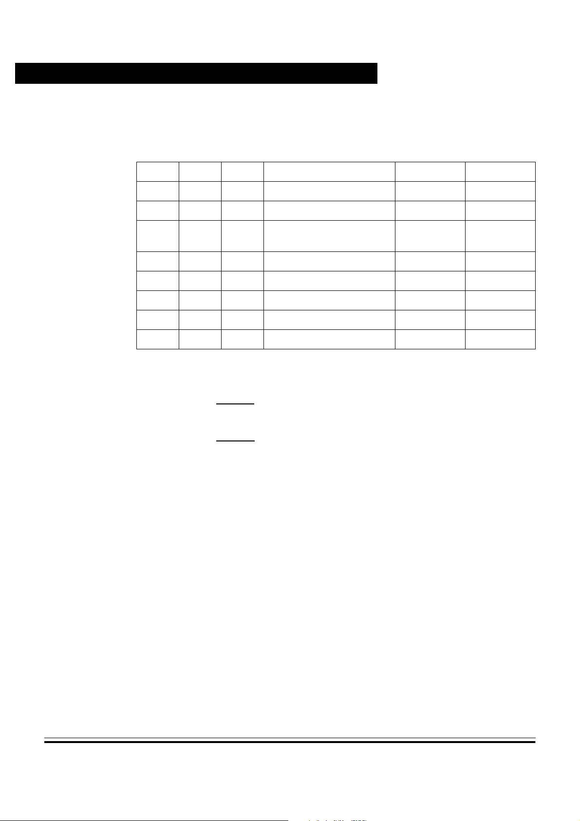
Operating Modes
BKGD MODB MODA Mode Port A Port B
Freescale Semiconductor, Inc.
Table 5-1. Mode Selection
1 0 0 Normal Single Chip G.P. I/O G.P. I/O
1 0 1 Normal Expanded Narrow ADDR/DATA ADDR
nc...
I
cale Semiconductor,
Frees
110
1 1 1 Normal Expanded Wide ADDR/DATA ADDR/DATA
0 0 0 Special Single Chip G.P. I/O G.P. I/O
0 0 1 Special Expanded Narrow ADDR/DATA ADDR
0 1 0 Special Peripheral ADDR/DATA ADDR/DATA
0 1 1 Speci al Expanded Wide ADDR/DATA A DDR/ DATA
Reserved (Forced to
Peripheral)
——
There are two basic types of operating modes:
Normal modes — some registers and bits are protected
against accidental changes.
Special modes — allow greater access to protected control
registers and bit s for special purposes such as test ing and
emulation.
For operation above 105°C, the MC68HC912DG128 (M temperature
range product only) is limited to single chip modes of operation.
A system development and debug feature, background debug mode
(BDM), is available in all modes. In special single-chip mode, BDM is
active immediately after reset.
5.3.1 Normal Operating Modes
These modes provide three operating configurations. Background
debugging is available in all three modes, but must first be enabled for
some operations by means of a BDM background command, then
activated.
Technical Data MC68HC912DG128 — Rev 3.0
76 Operating Modes MOTOROLA
For More Information On This Product,
Go to: www.freescale.com

Freescale Semiconductor, Inc.
nc...
I
Operating Modes
Operating Modes
Normal Single-Chip Mode — There are no external address
and data buses in this mode. The MCU operates as a standalone device and al l pro gram an d dat a reso urces are on- chip .
External port pins normally associated with address and data
buses can be used for general-purpose I/O.
Normal Expanded Wide Mode — This is a normal mode of
operation in which the expanded bus is present with a 16-bit
data bus. Ports A and B are used for the 16-bit multiplexed
address/data bus.
Normal Expanded Narrow Mode — This is a normal mode of
operation in which the expanded bus is present with an 8-bit
data bus. Ports A and B are used for the16-bit address bus.
Port A is used as t he da ta bu s, multi ple xed wi th add resses. In
this mode, 16-bit data is presented one byte at a time, the high
byte followed by t he low byte. The address is automatically
incremented on the second cycle.
5.3.2 Special Operating Modes
cale Semiconductor,
Frees
There are three special operating modes that correspond to normal
operating modes. Th ese operating mo des are commonly used in factory
testing and system development. In addition, there is a special
peripheral mode, i n which an external master , such as an I.C. tester, can
control the on-chip peripherals.
Special Single-Chip Mode — This mode can be us ed to force
the MCU to active BDM mode to allow system debug through
the BKGD pin. There are no external address and data buses
in this mode. The MCU oper ates as a st and-al one dev ice and
all program a nd data space are on-chip. External por t pins can
be used for general-purpose I/O.
Special Expanded Wide Mode — This mode can be us ed for
emulation of normal expanded wide mode and emulation of
normal single-chip mode. Ports A and B are used for the 16-bit
multiplexed address/data bus.
MC68HC912DG128 — Rev 3.0 Technical Data
MOTOROLA Operating Modes 77
For More Information On This Product,
Go to: www.freescale.com

Operating Modes
nc...
I
Freescale Semiconductor, Inc.
Special Expanded Narrow Mode — This mode can be used
for emulation of normal expanded narrow mode. Ports A and B
are used for the16-bit add ress bu s. Port A is use d as the da ta
bus, multiplexed with addresses. In this mode, 16-bit data is
presented one byte at a time, the high byte followed by the low
byte. The address is auto matically incremen ted on the second
cycle.
Special Peripheral Mode — The CPU is not active in this
mode. An external master can control on-chip peripherals for
testing purposes. It is not possible to change to or from this
mode without going through reset. Background debugging
should not be used while the MCU is in special peripheral
mode as internal bus conflicts be twee n BDM and the ext erna l
master can cause improper operation of both modes.
Bit 7654321Bit 0
SMODN MODB MODA ESTR IVIS EBSWAI EMK EME
RESET:00011011Special Single Chip
RESET:00111011Special Exp Nar
RESET:01011011Peripheral
RESET:01111011Special Exp Wide
RESET:10010000Normal Single Chip
RESET:10110000Normal Exp Nar
cale Semiconductor,
RESET:11110000Normal Exp Wide
MODE — Mode Register $000B
Frees
5.4 Background Debug Mode
Background debug mode (BDM) is an auxiliary operating mode that is
used for system devel opment. BDM is implemen ted in on-chip hardw are
and provides a full set of debug op erations. S ome BDM comm ands can
be executed while the CPU is operating normally. Other BDM
commands are firmware based, and require the BDM firmware to be
enabled and active for execution.
Technical Data MC68HC912DG128 — Rev 3.0
78 Operating Modes MOTOROLA
For More Information On This Product,
Go to: www.freescale.com

Freescale Semiconductor, Inc.
Operating Modes
Background Debug Mode
In special single-chip mode, BDM is ena bled and active immediately out
of reset. BDM is available in all other operating mode s, but must be
enabled before it can be activated. BDM should not be used in special
peripheral mode because of potential bus conflicts.
Once enabled, background mode can be made active by a serial
command sent via the BKGD pin or execution of a CPU12 BGND
instruction. While background mode is active, the CPU can interpret
special debugging commands, and read and write CPU registers,
peripheral registers, an d locations in memory.
While BDM is active, t he C PU execut es code located in a sm all o n-chip
nc...
I
ROM mapped to addresses $FF20 to $FFFF, and BDM control registers
are accessible at addresses $FF00 to $FF06. The BDM ROM replaces
the regular system vectors while BDM is active. While BDM is active, the
user memory from $FF00 to $FFFF is not in the map except through
serial BDM commands.
Bit 7654321Bit 0
SMODN MODB MODA ESTR IVIS EBSWAI 0 EME
RESET: 00011001Special Single Chip
RESET: 00111001Special Exp Nar
RESET: 01011001Peripheral
RESET: 01111001Special Exp Wide
cale Semiconductor,
Frees
RESET: 10010000Normal Single Chip
RESET: 10110000Normal Exp Nar
RESET: 11110000Normal Exp Wide
MODE — Mode Register $000B
The MODE register controls the MCU operating mode and various
configuration options. This register is not in the map in peripheral mode
SMODN, MODB, MODA — Mode Select Special, B and A
These bits show the current operatin g mode an d reflect the status of
the BKGD, MODB and MODA input pins at the rising edge of reset.
SMODN is Read anytime. May only be written in special mode s
(SMODN = 0). The first write is ignored;
MC68HC912DG128 — Rev 3.0 Technical Data
MOTOROLA Operating Modes 79
For More Information On This Product,
Go to: www.freescale.com

Operating Modes
Freescale Semiconductor, Inc.
MODB, MODA may be written once in Normal modes (SMODN = 1).
Write anytime in special modes (first write is ignored) – special
peripheral and reserved modes cannot be selected.
ESTR — E Clock Stretch Enable
Determines if the E Clock behaves as a simple free-running clock or
as a bus control signal that is active only for external bus cycles.
ESTR is always one in expanded modes since it is required for
address and dat a bus de-multiplexing and must follo w stretched
cycles.
0 = E never stretches (always free running).
nc...
I
cale Semiconductor,
Frees
1 = E stretches high during external access cycles and low during
non-visible internal accesses (IVIS = 0).
Normal modes: write once; Special modes: write anytime. Read
anytime.
IVIS — Internal Visibility
This bit determines whether internal ADDR, DATA, R/W an d L STR B
signals can be seen on the external bus during accesses to internal
locations. In Special Narrow Mode if this bit is set and an internal
access occurs the data will appear wide on Ports A and B. This serves
the same function as the EMD bit of the non-multiplexed versions of
the HC12 and allows for emulation. Visibility is not available when the
part is operating in a single-chip mode.
0 = No visibility of internal bus operations on external bus.
1 = Internal bus operations are visibl e on exte rn al bus.
Normal modes: write once; Special modes: write anytime EXCEPT
the first time. Read anytime.
Technical Data MC68HC912DG128 — Rev 3.0
80 Operating Modes MOTOROLA
For More Information On This Product,
Go to: www.freescale.com

Freescale Semiconductor, Inc.
EBSWAI — External Bus Module Stop in Wait Control
This bit controls access to the externa l bus inte rfa c e wh en in wait
mode. The module will delay before shutting down in wait mode to
allow for final bus activity to complete.
0 = External bus and registers continue functioning during wait
1 = External bus is shut down during wait mode.
Normal modes: write anytime; special modes: write never. Read
anytime.
EMK — Emulate Port K
Operating Modes
Internal Resource Mapping
mode.
nc...
I
5.5 Internal Resource Mapping
cale Semiconductor,
The internal register block, RAM, and EEPROM have default locations
within the 64K by te standard address space but may be reassigned to
Frees
other locations during program execution by setting bits in mapping
registers INITRG, INITRM, and INITEE. During n ormal operating modes
these registers c an be written once . I t is advisa ble to e xplicit ly establi sh
these resource locations during the initialization phase of program
execution, even if default values are chos en, in order to protect the
registers from inadvertent modification later.
In single-chip mode PORTK and DDRK are always in the map
regardless of the state of this bit.
0 = Port K and DDRK registers are in the mem o ry ma p. Memory
expansion emulation is disabled and all pins are general
purpose I/O.
1 = In expanded or peripheral mode, PORTK and DDRK are
removed from the internal memory map. Removing these
registers from the map allows th e user to em ulate th e function
of these registers externally.
Normal modes: write once; special modes: write anytime EXCEPT
the first time. Read anytime.
Writes to the mapping registers go into effect between the cycle that
follows the write and the cycle after that. To assure that there are no
MC68HC912DG128 — Rev 3.0 Technical Data
MOTOROLA Operating Modes 81
For More Information On This Product,
Go to: www.freescale.com

Operating Modes
nc...
I
cale Semiconductor,
Freescale Semiconductor, Inc.
unintended operations, a write to one of these registers should be
followed with a NOP instruction.
If conflicts occur when mapping resources, the register block will take
precedence over the other resources; RAM or EEPROM addresses
occupied by the register block will not be available for storage. When
active, BDM ROM takes precedence over other resources, although a
conflict between BDM ROM and register space is not possible. The
following table shows resource mapping precedence.
The MC68HC912DG128 contains 128K bytes of Flash EEPROM
nonvolatile memory which can be used to store program code or static
data. This physical memory comprises four 32k byte array modules,
00FEE32K, 01FEE32K, 10FE E32K and 11FEE32K. The 32K b yte array
11FEE32K has a fixed location from $4000 to $7FFF and $C000 to
$FFFF. The three 32K byte arrays 00FEE32K, 01FEE32K and
10FEE32K are accessible through a 16K byt e program page window
mapped from $8000 to $BFFF. The fixed 32K byte array 11FEE32K can
also be accessed through the program page window..
Table 5-2. Mapping Precedence
Precedence Resource
1 BDM ROM (if active)
2 Register Space
3RAM
4EEPROM
5 On-Chip Flash EEPROM
6 External Memory
Frees
5.5.1 Register Block Mapping
After reset the 1K byte register block resides at location $0000 but can
be reassigned to any 2K byte boundary within the standard 64K byte
address space. Mappin g o f inte r nal r eg ister s i s co ntr olled by fi ve b it s in
the INITRG register. The register block occupies the first 1K byte bytes
of the 2K byte block.
Technical Data MC68HC912DG128 — Rev 3.0
82 Operating Modes MOTOROLA
For More Information On This Product,
Go to: www.freescale.com

Freescale Semiconductor, Inc.
INITRG — Initialization of Internal Register Position Register $0011
Bit 7654321Bit 0
REG15 REG14 REG13 REG12 REG11 0 0 MMSWAI
RESET: 0 0000000
REG[15:11] — Internal register map position
These bits specify the upper five bits of the 16-bit registers address.
Normal modes: write once; special modes: write anytime. Read
anytime.
Operating Modes
Internal Resource Mapping
nc...
I
5.5.2 RAM Mapping
cale Semiconductor,
Frees
MMSWAI — Memory Mapping Interface Stop in Wait Control
This bit controls access to the memory ma pping interface when in
Wait mode.
Normal modes: write anytime; special modes: write never. Read
anytime.
0 = Memory mapping interface continues to function du ring Wait
mode.
1 = Memory mapping interface access is shut down during Wait
mode.
The MC68HC912DG128 has 8K bytes of fully static RAM that is used for
storing instructions, variables, and temporary data during program
execution. Since the RAM is actually implemented with two 4K RAM
arrays, any misaligned word access between last address of first 4K
RAM and first address of second 4K RAM will take two cycles instead of
one. After reset, RAM addressing begins at location $2000 but can be
assigned to any 8K byte boundary within the standard 64K byte address
space. Mapping of internal RAM is con trolled by three bits in the INITRM
register.
MC68HC912DG128 — Rev 3.0 Technical Data
MOTOROLA Operating Modes 83
For More Information On This Product,
Go to: www.freescale.com

Freescale Semiconductor, Inc.
Operating Modes
INITRM — Initialization of Internal RAM Position Register $0010
Bit 7654321Bit 0
RAM15 RAM14 RAM13 0 0 0 0 0
RESET: 0 0100000
RAM[15:13] — Internal RAM map position
These bits specify the upper three bits of the 16-bit RAM address.
Normal modes: write once; special modes: write anytime. Read
anytime.
nc...
I
5.5.3 EEPROM Mapping
The MC68HC912DG128 has 2K bytes of EEPROM which is activated by
the EEON bit in the INITEE register. Mapping of internal EEPROM is
controlled by four bits in the INITEE register. After reset EEPROM
address space begins at location $0800 but can be mapped to any 4K
byte boundary within the standard 64K byt e address space. The
EEPROM block occupies the last 2K bytes of the 4K byte block.
INITEE— Initialization of Internal EEPROM Position Register $0012
Bit 7654321Bit 0
EE15 EE14 EE13 EE12 0 0 0 EEON
RESET: 0 0000001
cale Semiconductor,
EE[15:12] — Internal EEPROM map position
These bits specify the up per fou r bits of t he 16-bit EEPROM a ddress.
Frees
Normal modes: write once; special modes: write anytime. Read
anytime.
EEON — internal EEPROM On (Enabled)
This bit is forced to one in single-chip modes.
Read or write anytime.
0 = Removes the EEPROM from the map.
1 = Places the on-chip EEPROM in the memory map at the address
selected by EE[15:12].
Technical Data MC68HC912DG128 — Rev 3.0
84 Operating Modes MOTOROLA
For More Information On This Product,
Go to: www.freescale.com

Freescale Semiconductor, Inc.
5.5.4 Flash EEPROM mapping through internal Memory Expansion
The Page Index register or PPAGE provides memory management for
the MC68HC912DG128. PPAGE consists of three bits to indicate which
physical location is active within the windows of the MC68HC912DG128.
The MC68HC912DG128 has a u ser’s program space window , a register
space window for Flash module registers, and a test program space
window.
The user’s program pa ge window consists of 1 6K Flash EEPROM bytes.
One of eight pages is viewed through this window for a total of 128K
accessible Flash EEPROM bytes.
Operating Modes
Internal Resource Mapping
nc...
I
cale Semiconductor,
Frees
5.5.5 Program space expansion
On the MC68HC912DG128, the register space window consists of a 4byte register block. One of four pages is viewed through this window for
each of the 32K flash module register blocks of MC68HC912DG128.
The test mode program page win dow consis t s of 32K Flash EEPR OM
bytes. One of the four 32K byte arrays is vie wed through this windo w for
a total 128K accessible Flash EEPROM bytes. This window is only
available in special mode for test purposes and replaces the user’s
program page window.
MC68HC912DG128 has a five pin port, Port K, for emulation and for
general purpose I/O. Three pins are used to emulate the three page
indices (PPAGE bits) and one pin is used as an emulation chip select.
When these four pins are not used for emulation they serve as general
purpose I/O pins. The fifth Port K pin is used as a general purpose I/O
pin.
There are 128K bytes of Flash EEPROM. With a 64K byte address
space, the PPAGE register is needed to perform on-chip memory
expansion. A program space window of 16K byte pages is located from
$8000 to $BFFF. Three page indices are used to point to one of eight
different 16K byte pages. They can be viewed as expanded addresses
x16, x15 and x14.
MC68HC912DG128 — Rev 3.0 Technical Data
MOTOROLA Operating Modes 85
For More Information On This Product,
Go to: www.freescale.com

Operating Modes
Freescale Semiconductor, Inc.
Table 5-3. Program space Page Index
Page Index 2
(PPAGE bit 2)
0 0 0 16K byte Page 0 00FEE32K
0 0 1 16K byte Page 1 00FEE32K
0 1 0 16K byte Page 2 01FEE32K
0 1 1 16K byte Page 3 01FEE32K
1 0 0 16K byte Page 4 10FEE32K
1 0 1 16K byte Page 5 10FEE32K
1 1 0 16K byte Page 6* 11FEE32K
1 1 1 16K byte Page 7* 11FEE32K
nc...
I
Page Index 1
(PPAGE bit 1)
* The 16K byte program space page 6 can also be accessed at a fixed
location from $4000 to $7FFF. The 16K byte program space page 7 can
also be accessed at a fixed location from $C000 to $FFFF.
5.5.6 Flash register space expansion
There are four 32K Flash arrays for MC68HC912DG128 and each
requires a 4-byte register block. A register space window is used to
access one of the four 4-byte blocks and the PPAGE register to map
each one into th e window. The register space window is located from
$00F4 to $00F7 after reset. Only two page indices are used to point to
one of the four pages of the register space.
cale Semiconductor,
Table 5-4. Flash Register space Page Index
Frees
Page Index 2
(PPAGE bit 2)
0 0 X $00F4-$00F7 Page 0 00FEE32K
0 1 X $00F4-$00F7 Page 1 01FEE32K
1 0 X $00F4-$00F7 Page 2 10FEE32K
1 1 X $00F4-$00F7 Page 3 11FEE32K
Page Index 1
(PPAGE bit 1)
Page Index 0
(PPAGE bit 0)
Page Index 0
(PPAGE bit 0)
16K Program space Page Flash array
Flash register space Page Flash array
Technical Data MC68HC912DG128 — Rev 3.0
86 Operating Modes MOTOROLA
For More Information On This Product,
Go to: www.freescale.com

Freescale Semiconductor, Inc.
5.5.7 Test mode Program space expansion
In special mode and for test purposes only, the 128K bytes of Flash
EEPROM can be accesse d through a test prog ram space window of 3 2K
bytes. This window replaces the user’s program space window to be
able to access an entire array. In special mode and with ROMTST bit set
in MISC register, a program space is located from $8000 to $FFFF. Only
two page indices are used to point to one of the four 32K byte arrays.
They can be viewed as expanded addresses X16 and X15.
Table 5-5. Test mode program space Page Index
nc...
I
Page Index 2
(PPAGE bit 2)
0 0 X 32K byte array Page 0 00FEE32K
0 1 X 32K byte array Page 1 01FEE32K
1 0 X 32K byte array Page 2 10FEE32K
1 1 X 32K byte array Page 3 11FEE32K
Page Index 1
(PPAGE bit 1)
Page Index 0
(PPAGE bit 0)
Operating Modes
Internal Resource Mapping
Flash register space Page Flash array
5.5.8 Page Index register descriptions
PORTK — Port K Data Register $00FC
Bit 7 6 5 4 3 2 1 Bit 0
PORT PK7 0 0 0 PK3 PK2 PK1 PK0
cale Semiconductor,
Frees
Emulation ECS 0 0 0 - PIX2 PIX1 PIX0
RESET: - 0 0 0 - - - -
Read and write anytime
Writing to the port does not change the pin states when it is configured
for page index emulation output.
This port is associated with the page index emulation pins. When the
port is not enabled to emulate page index, the port pins are used as
general-purpose I/O. Port K bit 3 is always a general purpose I/O pin.
This register i s not in the mem ory map in peripheral or expanded mo des
when the EMK control bit in MODE register is set.
MC68HC912DG128 — Rev 3.0 Technical Data
MOTOROLA Operating Modes 87
For More Information On This Product,
Go to: www.freescale.com

Operating Modes
Freescale Semiconductor, Inc.
When selected as inputs, these pins can be configured to be high
impedance or pulled up.
ECS — Emulation Chip Select of selected program space
When this signal is active low it indicates that the program space is
accessed. This also applies to test mode program spa ce. A n access
is made if an ad dr ess is in th e program space window an d ei the r the
Flash or external memory is accessed. The ECS timing is E clock high
and can be stretched when accessing external memory depending on
the EXTR0 and EXTR1 bits in the MISC register. The ECS signal is
only active when the EMK bit is set.
nc...
I
PIX[2:0] — The content of the PPAGE register emulated externally.
This content indicates which Flash module register space is in the
memory map and which 16K byte Flash memory is in the program
space. In special mode and with ROMTST bit set, the content of the
Page Index regi ster indicates whic h 32K byte Fl ash array is in the test
program space.
DDRK — Port K Data Direction Register $00FD
Bit 7 6 5 4 3 2 1 Bit 0
DDK7 0 0 0 DDK3 DDK2 DDK1 DDK0
RESET: 0 0 0 0 0 0 0 0
cale Semiconductor,
Read and write: anytime.
This register determines the primary direction for each port K pin
configured as general-purpose I/O.
Frees
0 = Associated pin is a high-impedance input.
1 = Associated pin is an output.
This register is n ot in the map in peri pheral or expanded mo des when the
EMK control bi t is set.
Technical Data MC68HC912DG128 — Rev 3.0
88 Operating Modes MOTOROLA
For More Information On This Product,
Go to: www.freescale.com

Freescale Semiconductor, Inc.
PPAGE — (Program) Page Index Register $00FF
Bit 7 6 5 4 3 2 1 Bit 0
0 0 0 0 0 PIX2 PIX1 PIX0
RESET: 0 0 0 0 0 0 0 0
Operating Modes
Internal Resource Mapping
Read and write: anytime.
This register determines the active page viewed through
MC68HC912DG128 windows.
CALL and RTC instructions have a special single wire mechanism to
nc...
I
read and write this register without using an addre ss bus.
5.5.9 Miscella neous System Control Register
Additional mapping and external resource controls are available. To use
external resources the part must be operated in one of the expanded
modes.
MISC — Miscellaneous Mapping Control Register $0013
Bit 7654321Bit 0Mode
ROMTST NDRF RFSTR1 RFSTR0 EXSTR1 EXSTR0 ROMHM ROMON
RESET: 0 0 0 0 1 1 0 0 Exp mode
RESET: 0 0 0 0 1 1 0 1
cale Semiconductor,
Normal modes: write once; Special modes: write anytime. Read
anytime.
Frees
ROMTST — FLASH EEPROM Test mode
In normal modes, this bit is forced to zero.
0 = 16K window for Flash memory is located from $8000–$BFFF
1 = 32K window for Flash memory is located from $8000–$FFFF
peripheral or
SC mode
MC68HC912DG128 — Rev 3.0 Technical Data
MOTOROLA Operating Modes 89
For More Information On This Product,
Go to: www.freescale.com

Operating Modes
nc...
I
Freescale Semiconductor, Inc.
NDRF — Narrow Data Bus for Register-Following Map Space
This bit enables a narrow bus feature for the 1K 512 byte RegisterFollowing Map. This is useful for accessing 8-bit peripherals and
allows 8-bit and 16-bit external memory devices to be mixed in a
system. In Expanded Narrow (eight bit) modes, Single Chip Modes,
and Peripheral mode, this bit has no effect.
0 = Makes Register-Follow ing MAP space act as a full 16 bit data bus.
1 = Makes the Register-Following MAP space act the same as an 8
bit only external data bus (data only goes through port A externally).
The Register-Following space is mapped from $0400 to $07FF after
reset, which is next to the register map. If th e registers are moved this
space follows.
cale Semiconductor,
Frees
RFSTR1, RFSTR0 — Register Following Stretch
This two bit field determines th e amount of clock str etch on accesses
to the 1K byte Register Following Map. It is valid regardless of the
state of the NDRF bit. In Single Chip and Peripheral Modes this bit
has no meaning or effect.
Table 5-6. RFSTR Stretch Bit Definition
RFSTR1 RFSTR0
00 0
01 1
10 2
11 3
Number of E Clocks
Stretched
Technical Data MC68HC912DG128 — Rev 3.0
90 Operating Modes MOTOROLA
For More Information On This Product,
Go to: www.freescale.com

Freescale Semiconductor, Inc.
EXSTR1, EXSTR0 — External Access Stretch
This two bit field determines th e amount of clock str etch on accesses
to the External Addre ss Space. In S ingle Ch ip and Per ipheral Modes
this bit has no meaning or effect .
Operating Modes
Internal Resource Mapping
Table 5-7. EXSTR Stretch Bit Definition
nc...
I
cale Semiconductor,
Frees
EXSTR1 EXSTR0
00 0
01 1
10 2
11 3
ROMHM — FLASH EEPROM only in second Half of Map
This bit has no mea ning if ROMON bit is clear.
0 = The 16K byte of fixed Flash EEPROM in location $4000–$7FFF
can be accessed.
1 = Disables direct access to 16K byte Flash EEPROM from
$4000–$7FFF in the memo ry ma p. The ph ysica l loca tion of
this16K byte Flash can still be accessed through the Program
Page window.
In special mode, with ROMTST bit set, this bit will allow overlap of the
four 32K Flash EEPROM arrays and overlap the four 4-byte Flash
register space in the same map space to be able to program all arrays
at the same time.
0 = The four 32K Flash arrays are accessed with four pages for
each.
1 = The four 32K Flash arrays coi ncide in th e same sp ace and a re
selected at the same time for programmin g.
Number of E Clocks
Stretched
CAUTION: Bit must be cleared before reading any of the arrays or registers.
ROMON — Enable FLASH EEPROM
These bits are used to enable the Flash EEPROM
0 = Disables Flash EEPRO M in the mem o ry ma p.
1 = Enables Flash EEPROM in the memory map.
MC68HC912DG128 — Rev 3.0 Technical Data
MOTOROLA Operating Modes 91
For More Information On This Product,
Go to: www.freescale.com

Freescale Semiconductor, Inc.
Operating Modes
5.5.10 Mapping test registers
These registers are u sed for testing the m apping logic. They ca n only be
read and after each read they get cleare d. A write to each register will
have no effect.
MTST0 — Mapping Test Register 0 $00F8
Bit 7654321Bit 0
MT07 MT06 MT05 MT04 MT03 MT02 MT01 MT00
RESET: 00000000
MTST1 — Mapping Test Register 1 $00F9
nc...
I
RESET: 00000000
Bit 7654321Bit 0
MT0F MT0E MT0D MT0C MT0B MT0A MT09 MT08
MTST2 — Mapping Test Register 2 $00FA
Bit 7654321Bit 0
RESET: 0 0 0 00000
MTST3 — Mapping Test Register 3 $00FB
RESET: 0 0 0 00000
MT17 MT16 MT15 MT14 MT13 MT12 MT11 MT10
Bit 7654321Bit 0
MT1F MT1E MT1D MT1C MT1B MT1A MT19 MT18
cale Semiconductor,
Frees
Technical Data MC68HC912DG128 — Rev 3.0
92 Operating Modes MOTOROLA
For More Information On This Product,
Go to: www.freescale.com

5.6 Memory Maps
Freescale Semiconductor, Inc.
Operating Modes
Memory Maps
The following diagrams illustrate the memory map for each mode of
operation immediately after reset.
$0000
$03FF
$0000
$0400
$0800
$1000
$2000
nc...
I
cale Semiconductor,
$4000
$8000
$C000
$FF00
$FFFF
SINGLE CHIP
EXT
VECTORSVECTORSVECTORS
EXPANDEDNORMAL
SPECIAL
SINGLE CHIP
$0800
$0FFF
$2000
$3FFF
$4000
$8000
$BFFF
$C000
$FFFF
$FF00
$FFFF
REGISTERS
(MAPPABLE TO ANY 2K SPACE)
2K bytes EEPROM
(MAPPABLE TO ANY 4K SPACE)
8K bytes RAM
(MAPPABLE TO ANY 8K SPACE)
16K Fixed Flash EEPROM
16K Page Window
Eight 16K Flash EEPROM pages
$A000 - $BFFF Protected BOOT
at odd programing pages
16K Fixed Flash EEPROM
$E000 - $FFFF Protected BOOT
BDM
(if active)
Frees
Figure 5-1. Memory Map after reset
The following diagram illustrates the memory paging scheme.
MC68HC912DG128 — Rev 3.0 Technical Data
MOTOROLA Operating Modes 93
For More Information On This Product,
Go to: www.freescale.com

Operating Modes
$0000
$0400
$0800
$1000
$2000
Freescale Semiconductor, Inc.
$4000
nc...
I
$8000
$C000
$E000
$FF00
$FFFF
cale Semiconductor,
6
16K Flash
(Paged)
7
(8K Boot)
VECTORS
NORMAL
SINGLE CHIP
16K Flash
(Unpaged)
16K Flash
(Unpaged)
One 16K Page accessible at a time (selected by PPAGE value = 0 to 7)
00 Flash 32K
0
1234567
(8K Boot) (8K Boot) (8K Boot) (8K Boot)
01 Flash 32K 10 Flash 32K 11 Flash 32K *
* This 32K Flash
accessible as
pages 6 & 7 and
as unpaged
$4000 - $7FFF &
$C000 - $FFFF
Figure 5-2. Memory Paging
Frees
Technical Data MC68HC912DG128 — Rev 3.0
94 Operating Modes MOTOROLA
For More Information On This Product,
Go to: www.freescale.com

Freescale Semiconductor, Inc.
Technical Data — MC68HC912DG128
Section 6. Bus Control and Input/Output
6.1 Contents
6.2 Introduction. . . . . . . . . . . . . . . . . . . . . . . . . . . . . . . . . . . . . . . . 95
6.3 Detecting Access Type from External Signals . . . . . . . . . . . . .95
nc...
I
6.4 Registers. . . . . . . . . . . . . . . . . . . . . . . . . . . . . . . . . . . . . . . . . .96
6.2 Introduction
Internally the MC68HC912DG128 has full 16-bit data paths, but
depending upon the operating mode and control registers, the external
multiplexed bus may be 8 or 16 bits. Ther e ar e cases wh ere 8- bi t and
16-bit accesses can appear on adjace nt cycles u sing the LSTRB signal
to indicate 8- or 16-bit data.
It is possible to have a mix of 8 and 16 bit peripherals attached to the
external multiplexed bus, using the NDRF bit in the MISC register while
in expanded wide modes.
cale Semiconductor,
6.3 Detecting Access Type from External Signals
Frees
The external signals L STRB, R/W, and A0 can be used to determin e the
type of bus access that is taking place. Accesses to the internal RAM
module are the only type of access that produce LSTRB =A0=1,
because the internal RAM is specifically designed to allow misaligned
16-bit accesses in a single cycle. In these cases the data for the address
MC68HC912DG128 — Rev 3.0 Technical Data
MOTOROLA Bus Control and Input/Output 95
For More Information On This Product,
Go to: www.freescale.com

Bus Control and Input/Output
that was accessed is on the low half of the data bus and the data for
address + 1 is on the high half of the data bus.
nc...
I
Freescale Semiconductor, Inc.
Figure 6-1. Access Type vs. Bus Control Pins
LSTRB A0 R/W Type of Access
1 0 1 8-bit read of an even address
0 1 1 8-bit read of an odd address
1 0 0 8-bit write of an even address
0 1 0 8-bit write of an odd address
0 0 1 16-bit read of an even address
111
0 0 0 16-bit write to an even address
110
16-bit read of an odd address
(low/high data swapped)
16-bit write to an even address
(low/high data swapped)
6.4 Registers
cale Semiconductor,
Frees
Not all registers are visible in the MC68HC912DG128 memory map
under certain conditi ons. In special peripheral mode the first 16 registe rs
associated with bus expansion are removed from the memory map.
In expanded modes, some or all of port A, port B, and port E are used
for expansion buses and control signals. In order to allow emulation of
the single-chip functions of these ports, some of these registers must be
rebuilt in an external port replacement unit. In any expanded mode, port
A, and port B, are used for ad dress and data lin es so regist ers for t hese
ports, as well as t he data direction registers for these ports, are removed
from the on-chip memory map and become external accesses.
In any expanded mode, port E pins m ay be needed for bus contro l (e.g.,
ECLK, R/W). To regain the single-chip functions of port E, the emulate
port E (EME) control bit in the MODE register may be set. In this special
case of expanded mo de and EME se t, PORTE and DDRE re gisters ar e
removed from the on-chip memory map and become external accesses
so port E may be rebuilt externally.
Technical Data MC68HC912DG128 — Rev 3.0
96 Bus Control and Input/Output MOTOROLA
For More Information On This Product,
Go to: www.freescale.com

Freescale Semiconductor, Inc.
Bit 7654321Bit 0
Single Chip PA7 PA6 PA5 PA4 PA3 PA2 PA1 PA0
RESET: ————————
Bus Control and Input/Output
Registers
Expanded
& Periph:
Expanded
narrow
PORTA — Port A Register $0000
nc...
I
ADDR15/
DATA15
ADDR15/
DATA15/
DATA7
ADDR14/
DATA14
ADDR14/
DATA14/
DATA6
ADDR13/
DATA13
ADDR13/
DATA13/
DATA5
ADDR12/
DATA12
ADDR12/
DATA12/
DATA4
ADDR11/
DATA11
ADDR11/
DATA11/
DATA3
ADDR10/
DATA10
ADDR10/
DATA10/
DATA2
ADDR9/
DATA9
ADDR9/
DATA9/
DATA1
ADDR8/
DATA8
ADDR8/
DATA8/
DATA0
Bits PA[7:0] are associated respectively with addresses ADDR[15:8],
DATA[15:8] and DATA[7 :0], in n arrow mo de. When this port i s not used
for external addresses such as in single-chip mode, these pins can be
used as general-purpose I/O. DDRA determines the primary directio n of
each pin. This regis ter is not in the on-chip map in ex panded and
peripheral modes. Read and write anytime.
Bit 7654321Bit 0
DDA7 DDA6 DDA5 DDA4 DDA3 DDA2 DDA1 DDA0
RESET: 0 0 0 0 0 0 0 0
DDRA — Port A Data Direction Register $0002
cale Semiconductor,
This register determines the primary direction for each port A pin when
functioning as a general-purpose I/O port. DDRA is not in the on-chip
Frees
map in expanded and peripheral modes. Read and write anytime.
0 = Associated pin is a high-impedance input
1 = Associated pin is an output
MC68HC912DG128 — Rev 3.0 Technical Data
MOTOROLA Bus Control and Input/Output 97
For More Information On This Product,
Go to: www.freescale.com

Freescale Semiconductor, Inc.
Bus Control and Input/Output
Bit 7654321Bit 0
Single Chip PB7 PB6 PB5 PB4 PB3 PB2 PB1 PB0
RESET: ————————
Expanded
& Periph:
Expanded
narrow
PORTB — Port B Register $0001
nc...
I
ADDR7/
DATA7
ADDR7 ADDR6 ADDR5 ADDR4 ADDR3 ADDR2 ADDR1 ADDR0
ADDR6/
DATA6
ADDR5/
DATA5
ADDR4/
DATA4
ADDR3/
DATA3
ADDR2/
DATA2
ADDR1/
DATA1
ADDR0/
DATA0
Bits PB[7:0] are associated with addresses ADDR[7:0] an d DATA[7:0]
(except in narrow mode) respectively. When this port is not used for
external addresses such as in single-chip mode, these pins can be used
as general-purpose I/O. DDRB determines the primary direction of each
pin. This register is not in the on-chip map in expanded and peripheral
modes. Read and write anyti me .
Bit 7654321Bit 0
DDB7 DDB6 DDB5 DDB4 DDB3 DDB2 DDB1 DDB0
RESET: 0 0 0 0 0 0 0 0
DDRB — Port B Data Direction Register $0003
cale Semiconductor,
This register determines the primary direction for each port B pin when
functioning as a general-purpose I/O port. DDRB is not in the on-chip
Frees
map in expanded and peripheral modes. Read and write anytime.
0 = Associated pin is a high-impedance input
1 = Associated pin is an output
Technical Data MC68HC912DG128 — Rev 3.0
98 Bus Control and Input/Output MOTOROLA
For More Information On This Product,
Go to: www.freescale.com

Freescale Semiconductor, Inc.
BIT 7654321BIT 0
PE7 PE6 PE5 PE4 PE3 PE2 PE1 PE0
RESET: ————————
or
Alt. Pin
Function
PORTE — Port E Register $0008
DBE
ECLK or
CAL
MODB or
IPIPE1 or
CGMTST
MODA or
IPIPE0
ECLK
LSTRB or
TAGLO
Bus Control and Input/Output
R/W IRQ XIRQ
This register is associated with exte rnal bus control signals and interr upt
nc...
I
inputs, including data bus enable (DBE), mode select (MODB/IPIPE1,
MODA/IPIPE0), E clock, size (LSTRB), read/write (R/W), IRQ, and
XIRQ. When the associated pin is not used for one of these specific
functions, the pin can be used as general-purpose I/O. The port E
assignment register (PEAR) selects the function of each pin. DDRE
determines the primary direction of each port E pin when configured to
be general-purpose I/O.
Some of these pi ns have software selectable pull-ups (DBE, LSTRB,
R/W, IRQ, and XIRQ). A single control bit enables the pull-ups for all
these pins which are configured as inputs.
This register is not in the map in peripheral mode or expanded modes
when the EME bit is set.
cale Semiconductor,
Read and write anytime.
Registers
Frees
MC68HC912DG128 — Rev 3.0 Technical Data
MOTOROLA Bus Control and Input/Output 99
For More Information On This Product,
Go to: www.freescale.com

Freescale Semiconductor, Inc.
Bus Control and Input/Output
Bit 7654321Bit 0
DDE7 DDE6 DDE5 DDE4 DDE3 DDE2 0 0
RESET: 0 0 000000
DDRE — Port E Data Direction Register $0009
This register determines the primary direction for each port E pin
configured as general-purpose I/O.
0 = Associated pin is a high-impedance input
nc...
I
1 = Associated pin is an output
PE[1:0] are associated with XIRQ and IRQ and cannot be configured as
outputs. These pins can be read regardless of whether the alternate
interrupt functions are enabled.
This register is not in th e map in peripher al mode and expanded m odes
while the EME control bit is set.
Read and write anytime.
BIT 7654321BIT 0
NDBE CGMTE PIPOE NECLK LSTRE RDWE CALE DBENE
cale Semiconductor,
RESET: 0 0 0 0 0 0 0 0
RESET: 0 0 1 0 1 1 0 0
Frees
RESET: 1 1 0 1 0 0 0 0 Peripheral
RESET: 1 0 0 1 0 0 0 0
RESET: 0 0 1 0 1 1 0 0
PEAR — Port E Assignment Register $000A
Normal
Expanded
Special
Expanded
Normal
single chip
Special
single chip
The PEAR register is used to choose between th e ge nera l-purpo se I/O
functions and the alternate bus control functions of Port E. When an
Technical Data MC68HC912DG128 — Rev 3.0
100 Bus Control and Input/Output MOTOROLA
For More Information On This Product,
Go to: www.freescale.com
 Loading...