


Freescale Semiconductor, Inc.
MC68HC908JB8
MC68HC08JB8
nc...
I
cale Semiconductor,
Frees
M68HC08
Microcontrollers
MC68HC08JT8
Technical Data
MC68HC908JB8/D
Rev. 2.1, 12/2003
MOTOROLA.COM/SEMICONDUCTORS
For More Information On This Product,
Go to: www.freescale.com

Freescale Semiconductor, Inc.
nc...
I
cale Semiconductor,
Frees
For More Information On This Product,
Go to: www.freescale.com

Freescale Semiconductor, Inc.
MC68HC908JB8
MC68HC08JB8
nc...
I
cale Semiconductor,
Frees
MC68HC08JT8
Technical Data
To provide the most up-to-date information, the revision of our
documents on the World Wide Web will be the most current. Your printed
copy may be an earlier revision. To verify you have the latest information
available, refer to:
http://motorola.com/semiconductors/
The following revision history table summarizes changes contained in
this document. For your convenience, the page number designators
have been linked to the appropriate location.
Motorola and the Stylized M Logo are registered trademarks of Motorola, Inc.
DigitalDNA is a trademark of Motorola, Inc.
This product incorporates SuperFlash® technology licensed from SST. © Motorola, Inc., 2003
MC68HC908JB8•MC68HC08JB8•MC68HC08JT8 — Rev. 2.1 Technical Data
MOTOROLA 3
For More Information On This Product,
Go to: www.freescale.com
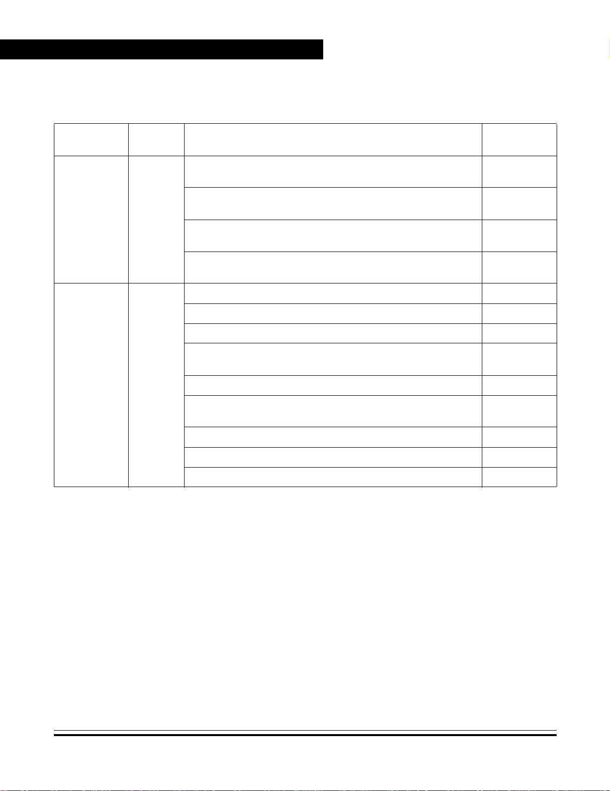
Revision History
Freescale Semiconductor, Inc.
Revision History
Date
December
2003
nc...
I
February,
2002
Revision
Level
2.1
2
Description
4.9 ROM-Resident Routines — Removed block erase
references for ROM-resident routines.
9.8.8 USB Control Register 3 — Clarified bit descriptions for
OSTALL0 and ISTALL0.
9.8.11 USB Status Register 1 — Clarified bit descriptions for
TXACK, TXNAK, and TXSTL.
Section 19. Mechanical Specifications — Replaced incorrect
44-pin QFP drawing, case 824E to case 824A.
Corrected PTD6 and PTD7: not direct LED drive pins. 28, 210, 217
Removed incorrect RX1E text from USB control register 1. 146
Corrected Figure 9-30 for USB module. 159
Corrected timer discrepancies throughout Section 11. Timer
Interface Module (TIM).
Added Table 12-1 . Port Control Register Bits Summary. 201
Changed pullup resistor limits for D– and I/O ports in
18.6 DC Electrical Characteristics.
Added mechanical drawing for 20-pin SOIC package. 266
Added Appendix A. MC68HC08JB8 — ROM part. 269
Added Appendix B. MC68HC08JT8 — low-voltage ROM part. 277
cale Semiconductor,
Page
Number(s)
61
149, 150
153
263
177
256
Frees
Technical Data MC68HC908JB8•MC68HC08JB8•MC68HC08JT8 — Rev. 2.1
4 MOTOROLA
For More Information On This Product,
Go to: www.freescale.com

Freescale Semiconductor, Inc.
Technical Data – MC68HC908JB8•MC68HC08JB8•MC68HC08JT8
List of Sections
Section 1. General Description . . . . . . . . . . . . . . . . . . . . 27
Section 2. Memory Map . . . . . . . . . . . . . . . . . . . . . . . . . . 39
Section 3. Random-Access Memory (RAM) . . . . . . . . . . 51
nc...
I
cale Semiconductor,
Frees
Section 4. FLASH Memory . . . . . . . . . . . . . . . . . . . . . . . .53
Section 5. Configuration Register (CONFIG) . . . . . . . . .65
Section 6. Central Processor Unit (CPU) . . . . . . . . . . . . 69
Section 7. Oscillator (OSC) . . . . . . . . . . . . . . . . . . . . . . .89
Section 8. System Integration Module (SIM) . . . . . . . . .93
Section 9. Universal Serial Bus Module (USB). . . . . . . 117
Section 10. Monitor ROM (MON) . . . . . . . . . . . . . . . . . . 163
Section 11. Timer Interface Module (TIM) . . . . . . . . . . .177
Section 12. Input/Output Ports (I/O) . . . . . . . . . . . . . . . 199
Section 13. External Interrupt (IRQ) . . . . . . . . . . . . . . .219
Section 14. Keyboard Interrupt Module (KBI). . . . . . . . 227
Section 15. Computer Operating Properly (COP) . . . .237
Section 16. Low Voltage Inhibit (LVI) . . . . . . . . . . . . . .243
Section 17. Break Module (BREAK) . . . . . . . . . . . . . . .245
Section 18. Electrical Specifications. . . . . . . . . . . . . . . 253
Section 19. Mechanical Specifications . . . . . . . . . . . . .263
Section 20. Ordering Information . . . . . . . . . . . . . . . . . 267
Appendix A. MC68HC08JB8. . . . . . . . . . . . . . . . . . . . . . 269
Appendix B. MC68HC08JT8 . . . . . . . . . . . . . . . . . . . . . .277
MC68HC908JB8•MC68HC08JB8•MC68HC08JT8 — Rev. 2.1 Technical Data
MOTOROLA List of Sections 5
For More Information On This Product,
Go to: www.freescale.com

Freescale Semiconductor, Inc.
List of Sections
nc...
I
cale Semiconductor,
Frees
Technical Data MC68HC908JB8•MC68HC08JB8•MC68HC08JT8 — Rev. 2.1
6 List of Sections MOTOROLA
For More Information On This Product,
Go to: www.freescale.com

Freescale Semiconductor, Inc.
Technical Data – MC68HC908JB8•MC68HC08JB8•MC68HC08JT8
Table of Contents
Section 1. General Description
1.1 Contents . . . . . . . . . . . . . . . . . . . . . . . . . . . . . . . . . . . . . . . . . .27
1.2 Introduction. . . . . . . . . . . . . . . . . . . . . . . . . . . . . . . . . . . . . . . .27
nc...
I
cale Semiconductor,
Frees
1.3 Features . . . . . . . . . . . . . . . . . . . . . . . . . . . . . . . . . . . . . . . . . .28
1.4 MCU Block Diagram . . . . . . . . . . . . . . . . . . . . . . . . . . . . . . . . .30
1.5 Pin Assignments. . . . . . . . . . . . . . . . . . . . . . . . . . . . . . . . . . . .32
1.5.1 Power Supply Pins (VDD, VSS) . . . . . . . . . . . . . . . . . . . . . . . 34
1.5.2 Voltage Regulator Out (V
1.5.3 Oscillator Pins (OSC1 and OSC2) . . . . . . . . . . . . . . . . . . . .35
1.5.4 External Reset Pin (RST) . . . . . . . . . . . . . . . . . . . . . . . . . . . 35
1.5.5 External Interrupt Pins (IRQ, PTE4/D–) . . . . . . . . . . . . . . . .35
1.5.6 Port A Input/Output (I/O) Pins (PTA7/KBA7–PTA0/KBA0). .36
1.5.7 Port B (I/O) Pins (PTB7–PTB0) . . . . . . . . . . . . . . . . . . . . . . 36
1.5.8 Port C I/O Pins (PTC7–PTC0) . . . . . . . . . . . . . . . . . . . . . . . 36
1.5.9 Port D I/O Pins (PTD7–PTD0) . . . . . . . . . . . . . . . . . . . . . . . 36
1.5.10 Port E I/O Pins (PTE4/D–, PTE3/D+, PTE2/TCH1,
PTE1/TCH0, PTE0/TCLK). . . . . . . . . . . . . . . . . . . . . . . . 36
) . . . . . . . . . . . . . . . . . . . . . . .34
REG
Section 2. Memory Map
2.1 Contents . . . . . . . . . . . . . . . . . . . . . . . . . . . . . . . . . . . . . . . . . .39
2.2 Introduction. . . . . . . . . . . . . . . . . . . . . . . . . . . . . . . . . . . . . . . .39
2.3 I/O Section . . . . . . . . . . . . . . . . . . . . . . . . . . . . . . . . . . . . . . . .41
2.4 Monitor ROM . . . . . . . . . . . . . . . . . . . . . . . . . . . . . . . . . . . . . .41
MC68HC908JB8•MC68HC08JB8•MC68HC08JT8 — Rev. 2.1 Technical Data
MOTOROLA Table of Contents 7
For More Information On This Product,
Go to: www.freescale.com

Table of Contents
Freescale Semiconductor, Inc.
Section 3. Random-Access Memory (RAM)
3.1 Contents . . . . . . . . . . . . . . . . . . . . . . . . . . . . . . . . . . . . . . . . . .51
3.2 Introduction. . . . . . . . . . . . . . . . . . . . . . . . . . . . . . . . . . . . . . . .51
3.3 Functional Description . . . . . . . . . . . . . . . . . . . . . . . . . . . . . . .51
Section 4. FLASH Memory
4.1 Contents . . . . . . . . . . . . . . . . . . . . . . . . . . . . . . . . . . . . . . . . . .53
4.2 Introduction. . . . . . . . . . . . . . . . . . . . . . . . . . . . . . . . . . . . . . . .53
nc...
I
cale Semiconductor,
Frees
4.3 Functional Description . . . . . . . . . . . . . . . . . . . . . . . . . . . . . . .54
4.4 FLASH Control Register . . . . . . . . . . . . . . . . . . . . . . . . . . . . . .55
4.5 FLASH Block Erase Operation . . . . . . . . . . . . . . . . . . . . . . . . .56
4.6 FLASH Mass Erase Operation . . . . . . . . . . . . . . . . . . . . . . . . .57
4.7 FLASH Program Operation. . . . . . . . . . . . . . . . . . . . . . . . . . . .58
4.8 FLASH Protection. . . . . . . . . . . . . . . . . . . . . . . . . . . . . . . . . . .60
4.8.1 FLASH Block Protect Register . . . . . . . . . . . . . . . . . . . . . . .60
4.9 ROM-Resident Routines. . . . . . . . . . . . . . . . . . . . . . . . . . . . . .61
4.9.1 Variables . . . . . . . . . . . . . . . . . . . . . . . . . . . . . . . . . . . . . . .62
4.9.2 ERASE Routine . . . . . . . . . . . . . . . . . . . . . . . . . . . . . . . . . . 62
4.9.3 PROGRAM Routine . . . . . . . . . . . . . . . . . . . . . . . . . . . . . . .63
4.9.4 VERIFY Routine . . . . . . . . . . . . . . . . . . . . . . . . . . . . . . . . . . 63
Section 5. Configuration Register (CONFIG)
5.1 Contents . . . . . . . . . . . . . . . . . . . . . . . . . . . . . . . . . . . . . . . . . .65
5.2 Introduction. . . . . . . . . . . . . . . . . . . . . . . . . . . . . . . . . . . . . . . .65
5.3 Functional Description . . . . . . . . . . . . . . . . . . . . . . . . . . . . . . .66
Technical Data MC68HC908JB8•MC68HC08JB8•MC68HC08JT8 — Rev. 2.1
8 Table of Contents MOTOROLA
For More Information On This Product,
Go to: www.freescale.com

Freescale Semiconductor, Inc.
Table of Contents
Section 6. Central Processor Unit (CPU)
6.1 Contents . . . . . . . . . . . . . . . . . . . . . . . . . . . . . . . . . . . . . . . . . .69
6.2 Introduction. . . . . . . . . . . . . . . . . . . . . . . . . . . . . . . . . . . . . . . .70
6.3 Features . . . . . . . . . . . . . . . . . . . . . . . . . . . . . . . . . . . . . . . . . .70
6.4 CPU Registers . . . . . . . . . . . . . . . . . . . . . . . . . . . . . . . . . . . . .71
6.4.1 Accumulator . . . . . . . . . . . . . . . . . . . . . . . . . . . . . . . . . . . . .71
6.4.2 Index Register . . . . . . . . . . . . . . . . . . . . . . . . . . . . . . . . . . .72
6.4.3 Stack Pointer . . . . . . . . . . . . . . . . . . . . . . . . . . . . . . . . . . . . 72
6.4.4 Program Counter . . . . . . . . . . . . . . . . . . . . . . . . . . . . . . . . .73
6.4.5 Condition Code Register . . . . . . . . . . . . . . . . . . . . . . . . . . . 74
nc...
I
6.5 Arithmetic/Logic Unit (ALU) . . . . . . . . . . . . . . . . . . . . . . . . . . .76
cale Semiconductor,
Frees
6.6 Low-Power Modes . . . . . . . . . . . . . . . . . . . . . . . . . . . . . . . . . .76
6.6.1 Wait Mode . . . . . . . . . . . . . . . . . . . . . . . . . . . . . . . . . . . . . .76
6.6.2 Stop Mode . . . . . . . . . . . . . . . . . . . . . . . . . . . . . . . . . . . . . .77
6.7 CPU During Break Interrupts . . . . . . . . . . . . . . . . . . . . . . . . . .77
6.8 Instruction Set Summary . . . . . . . . . . . . . . . . . . . . . . . . . . . . .78
6.9 Opcode Map . . . . . . . . . . . . . . . . . . . . . . . . . . . . . . . . . . . . . . . 86
Section 7. Oscillator (OSC)
7.1 Contents . . . . . . . . . . . . . . . . . . . . . . . . . . . . . . . . . . . . . . . . . .89
7.2 Introduction. . . . . . . . . . . . . . . . . . . . . . . . . . . . . . . . . . . . . . . .89
7.3 Oscillator External Connections . . . . . . . . . . . . . . . . . . . . . . . .90
7.4 I/O Signals . . . . . . . . . . . . . . . . . . . . . . . . . . . . . . . . . . . . . . . . 91
7.4.1 Crystal Amplifier Input Pin (OSC1). . . . . . . . . . . . . . . . . . . . 91
7.4.2 Crystal Amplifier Output Pin (OSC2) . . . . . . . . . . . . . . . . . . 91
7.4.3 Oscillator Enable Signal (SIMOSCEN). . . . . . . . . . . . . . . . . 91
7.4.4 External Clock Source (OSCXCLK) . . . . . . . . . . . . . . . . . . . 91
7.4.5 Oscillator Out (OSCOUT). . . . . . . . . . . . . . . . . . . . . . . . . . . 92
7.5 Low-Power Modes . . . . . . . . . . . . . . . . . . . . . . . . . . . . . . . . . .92
7.5.1 Wait Mode . . . . . . . . . . . . . . . . . . . . . . . . . . . . . . . . . . . . . .92
7.5.2 Stop Mode . . . . . . . . . . . . . . . . . . . . . . . . . . . . . . . . . . . . . .92
7.6 Oscillator During Break Mode. . . . . . . . . . . . . . . . . . . . . . . . . .92
MC68HC908JB8•MC68HC08JB8•MC68HC08JT8 — Rev. 2.1 Technical Data
MOTOROLA Table of Contents 9
For More Information On This Product,
Go to: www.freescale.com

nc...
I
cale Semiconductor,
Frees
Table of Contents
Freescale Semiconductor, Inc.
Section 8. System Integration Module (SIM)
8.1 Contents . . . . . . . . . . . . . . . . . . . . . . . . . . . . . . . . . . . . . . . . . .93
8.2 Introduction. . . . . . . . . . . . . . . . . . . . . . . . . . . . . . . . . . . . . . . .94
8.3 SIM Bus Clock Control and Generation . . . . . . . . . . . . . . . . . .96
8.3.1 Bus Timing . . . . . . . . . . . . . . . . . . . . . . . . . . . . . . . . . . . . . .97
8.3.2 Clock Startup from POR or LVI Reset . . . . . . . . . . . . . . . . . 97
8.3.3 Clocks in Stop Mode and Wait Mode . . . . . . . . . . . . . . . . . .97
8.4 Reset and System Initialization. . . . . . . . . . . . . . . . . . . . . . . . .97
8.4.1 External Pin Reset . . . . . . . . . . . . . . . . . . . . . . . . . . . . . . . . 98
8.4.2 Active Resets from Internal Sources . . . . . . . . . . . . . . . . . . 99
8.4.2.1 Power-On Reset . . . . . . . . . . . . . . . . . . . . . . . . . . . . . .100
8.4.2.2 Computer Operating Properly (COP) Reset. . . . . . . . . .101
8.4.2.3 Illegal Opcode Reset . . . . . . . . . . . . . . . . . . . . . . . . . . . 101
8.4.2.4 Illegal Address Reset . . . . . . . . . . . . . . . . . . . . . . . . . . . 101
8.4.2.5 Low-Voltage Inhibit (LVI) Reset . . . . . . . . . . . . . . . . . . . 102
8.4.2.6 Universal Serial Bus Reset . . . . . . . . . . . . . . . . . . . . . .102
8.4.2.7 Registers Values After Different Resets. . . . . . . . . . . . . 102
8.5 SIM Counter . . . . . . . . . . . . . . . . . . . . . . . . . . . . . . . . . . . . . .103
8.5.1 SIM Counter During Power-On Reset . . . . . . . . . . . . . . . . 103
8.5.2 SIM Counter During Stop Mode Recovery . . . . . . . . . . . . . 104
8.5.3 SIM Counter and Reset States. . . . . . . . . . . . . . . . . . . . . .104
8.6 Exception Control . . . . . . . . . . . . . . . . . . . . . . . . . . . . . . . . . .104
8.6.1 Interrupts . . . . . . . . . . . . . . . . . . . . . . . . . . . . . . . . . . . . . . 104
8.6.1.1 Hardware Interrupts . . . . . . . . . . . . . . . . . . . . . . . . . . . . 107
8.6.1.2 SWI Instruction. . . . . . . . . . . . . . . . . . . . . . . . . . . . . . . . 108
8.6.2 Interrupt Status Registers. . . . . . . . . . . . . . . . . . . . . . . . . . 108
8.6.2.1 Interrupt Status Register 1 . . . . . . . . . . . . . . . . . . . . . . . 109
8.6.3 Reset . . . . . . . . . . . . . . . . . . . . . . . . . . . . . . . . . . . . . . . . . 109
8.6.4 Break Interrupts . . . . . . . . . . . . . . . . . . . . . . . . . . . . . . . . .109
8.6.5 Status Flag Protection in Break Mode . . . . . . . . . . . . . . . . 110
8.7 Low-Power Modes . . . . . . . . . . . . . . . . . . . . . . . . . . . . . . . . .110
8.7.1 Wait Mode . . . . . . . . . . . . . . . . . . . . . . . . . . . . . . . . . . . . .110
8.7.2 Stop Mode . . . . . . . . . . . . . . . . . . . . . . . . . . . . . . . . . . . . .112
8.8 SIM Registers . . . . . . . . . . . . . . . . . . . . . . . . . . . . . . . . . . . . .113
Technical Data MC68HC908JB8•MC68HC08JB8•MC68HC08JT8 — Rev. 2.1
10 Table of Contents MOTOROLA
For More Information On This Product,
Go to: www.freescale.com

Freescale Semiconductor, Inc.
8.8.1 Break Status Register . . . . . . . . . . . . . . . . . . . . . . . . . . . .113
8.8.2 Reset Status Register . . . . . . . . . . . . . . . . . . . . . . . . . . . .114
8.8.3 Break Flag Control Register . . . . . . . . . . . . . . . . . . . . . . . 116
Table of Contents
Section 9. Universal Serial Bus Module (USB)
9.1 Contents . . . . . . . . . . . . . . . . . . . . . . . . . . . . . . . . . . . . . . . . .117
9.2 Introduction. . . . . . . . . . . . . . . . . . . . . . . . . . . . . . . . . . . . . . .118
9.3 Features . . . . . . . . . . . . . . . . . . . . . . . . . . . . . . . . . . . . . . . . .119
9.4 Pin Name Conventions. . . . . . . . . . . . . . . . . . . . . . . . . . . . . .120
nc...
I
cale Semiconductor,
Frees
9.5 Functional Description . . . . . . . . . . . . . . . . . . . . . . . . . . . . . .124
9.5.1 USB Protocol . . . . . . . . . . . . . . . . . . . . . . . . . . . . . . . . . . . 125
9.5.1.1 Sync Pattern . . . . . . . . . . . . . . . . . . . . . . . . . . . . . . . . .126
9.5.1.2 Packet Identifier Field . . . . . . . . . . . . . . . . . . . . . . . . . .127
9.5.1.3 Address Field (ADDR) . . . . . . . . . . . . . . . . . . . . . . . . . .128
9.5.1.4 Endpoint Field (ENDP). . . . . . . . . . . . . . . . . . . . . . . . . .128
9.5.1.5 Cyclic Redundancy Check (CRC) . . . . . . . . . . . . . . . . .128
9.5.1.6 End-of-Packet (EOP) . . . . . . . . . . . . . . . . . . . . . . . . . . . 128
9.5.2 Reset Signaling . . . . . . . . . . . . . . . . . . . . . . . . . . . . . . . . .129
9.5.3 Suspend . . . . . . . . . . . . . . . . . . . . . . . . . . . . . . . . . . . . . . .130
9.5.4 Resume After Suspend . . . . . . . . . . . . . . . . . . . . . . . . . . .131
9.5.4.1 Host Initiated Resume . . . . . . . . . . . . . . . . . . . . . . . . . . 131
9.5.4.2 USB Reset Signalling. . . . . . . . . . . . . . . . . . . . . . . . . . .131
9.5.4.3 Remote Wakeup . . . . . . . . . . . . . . . . . . . . . . . . . . . . . .131
9.5.5 Low-Speed Device . . . . . . . . . . . . . . . . . . . . . . . . . . . . . . .132
9.6 Clock Requirements . . . . . . . . . . . . . . . . . . . . . . . . . . . . . . . .132
9.7 Hardware Description . . . . . . . . . . . . . . . . . . . . . . . . . . . . . . .133
9.7.1 Voltage Regulator. . . . . . . . . . . . . . . . . . . . . . . . . . . . . . . . 133
9.7.2 USB Transceiver . . . . . . . . . . . . . . . . . . . . . . . . . . . . . . . .133
9.7.2.1 Output Driver Characteristics. . . . . . . . . . . . . . . . . . . . .134
9.7.2.2 Low Speed (1.5 Mbps) Driver Characteristics . . . . . . . .134
9.7.2.3 Receiver Data Jitter . . . . . . . . . . . . . . . . . . . . . . . . . . . .135
9.7.2.4 Data Source Jitter . . . . . . . . . . . . . . . . . . . . . . . . . . . . . 135
9.7.2.5 Data Signal Rise and Fall Time . . . . . . . . . . . . . . . . . . .136
9.7.3 USB Control Logic . . . . . . . . . . . . . . . . . . . . . . . . . . . . . . . 137
MC68HC908JB8•MC68HC08JB8•MC68HC08JT8 — Rev. 2.1 Technical Data
MOTOROLA Table of Contents 11
For More Information On This Product,
Go to: www.freescale.com

Freescale Semiconductor, Inc.
Table of Contents
9.8 I/O Registers. . . . . . . . . . . . . . . . . . . . . . . . . . . . . . . . . . . . . .137
9.8.1 USB Address Register . . . . . . . . . . . . . . . . . . . . . . . . . . . .138
9.8.2 USB Interrupt Register 0 . . . . . . . . . . . . . . . . . . . . . . . . . . 139
9.8.3 USB Interrupt Register 1 . . . . . . . . . . . . . . . . . . . . . . . . . . 141
9.8.4 USB Interrupt Register 2 . . . . . . . . . . . . . . . . . . . . . . . . . . 144
9.8.5 USB Control Register 0 . . . . . . . . . . . . . . . . . . . . . . . . . . . 145
9.8.6 USB Control Register 1 . . . . . . . . . . . . . . . . . . . . . . . . . . . 146
9.8.7 USB Control Register 2 . . . . . . . . . . . . . . . . . . . . . . . . . . . 147
9.8.8 USB Control Register 3 . . . . . . . . . . . . . . . . . . . . . . . . . . . 149
9.8.9 USB Control Register 4 . . . . . . . . . . . . . . . . . . . . . . . . . . . 151
9.8.10 USB Status Register 0 . . . . . . . . . . . . . . . . . . . . . . . . . . . .152
nc...
I
9.8.11 USB Status Register 1 . . . . . . . . . . . . . . . . . . . . . . . . . . . .153
9.8.12 USB Endpoint 0 Data Registers . . . . . . . . . . . . . . . . . . . . . 154
9.8.13 USB Endpoint 1 Data Registers . . . . . . . . . . . . . . . . . . . . . 155
9.8.14 USB Endpoint 2 Data Registers . . . . . . . . . . . . . . . . . . . . . 156
cale Semiconductor,
Frees
9.9 USB Interrupts . . . . . . . . . . . . . . . . . . . . . . . . . . . . . . . . . . . .157
9.9.1 USB End-of-Transaction Interrupt . . . . . . . . . . . . . . . . . . . 157
9.9.1.1 Receive Control Endpoint 0 . . . . . . . . . . . . . . . . . . . . . . 158
9.9.1.2 Transmit Control Endpoint 0 . . . . . . . . . . . . . . . . . . . . .160
9.9.1.3 Transmit Endpoint 1. . . . . . . . . . . . . . . . . . . . . . . . . . . .161
9.9.1.4 Transmit Endpoint 2. . . . . . . . . . . . . . . . . . . . . . . . . . . .162
9.9.1.5 Receive Endpoint 2 . . . . . . . . . . . . . . . . . . . . . . . . . . . . 162
9.9.2 Resume Interrupt . . . . . . . . . . . . . . . . . . . . . . . . . . . . . . . . 162
9.9.3 End-of-Packet Interrupt . . . . . . . . . . . . . . . . . . . . . . . . . . .162
Section 10. Monitor ROM (MON)
10.1 Contents . . . . . . . . . . . . . . . . . . . . . . . . . . . . . . . . . . . . . . . . .163
10.2 Introduction. . . . . . . . . . . . . . . . . . . . . . . . . . . . . . . . . . . . . . .163
10.3 Features . . . . . . . . . . . . . . . . . . . . . . . . . . . . . . . . . . . . . . . . .164
10.4 Functional Description . . . . . . . . . . . . . . . . . . . . . . . . . . . . . .164
10.4.1 Entering Monitor Mode . . . . . . . . . . . . . . . . . . . . . . . . . . . .166
10.4.2 Baud Rate . . . . . . . . . . . . . . . . . . . . . . . . . . . . . . . . . . . . .169
10.4.3 Data Format . . . . . . . . . . . . . . . . . . . . . . . . . . . . . . . . . . . .170
10.4.4 Echoing . . . . . . . . . . . . . . . . . . . . . . . . . . . . . . . . . . . . . . .170
10.4.5 Break Signal . . . . . . . . . . . . . . . . . . . . . . . . . . . . . . . . . . . .171
Technical Data MC68HC908JB8•MC68HC08JB8•MC68HC08JT8 — Rev. 2.1
12 Table of Contents MOTOROLA
For More Information On This Product,
Go to: www.freescale.com

Freescale Semiconductor, Inc.
10.4.6 Commands . . . . . . . . . . . . . . . . . . . . . . . . . . . . . . . . . . . . .171
10.5 Security. . . . . . . . . . . . . . . . . . . . . . . . . . . . . . . . . . . . . . . . . .175
Table of Contents
Section 11. Timer Interface Module (TIM)
11.1 Contents . . . . . . . . . . . . . . . . . . . . . . . . . . . . . . . . . . . . . . . . .177
11.2 Introduction. . . . . . . . . . . . . . . . . . . . . . . . . . . . . . . . . . . . . . .178
11.3 Features . . . . . . . . . . . . . . . . . . . . . . . . . . . . . . . . . . . . . . . . .178
11.4 Pin Name Conventions. . . . . . . . . . . . . . . . . . . . . . . . . . . . . .178
nc...
I
cale Semiconductor,
Frees
11.5 Functional Description . . . . . . . . . . . . . . . . . . . . . . . . . . . . . .179
11.5.1 TIM Counter Prescaler . . . . . . . . . . . . . . . . . . . . . . . . . . . . 181
11.5.2 Input Capture . . . . . . . . . . . . . . . . . . . . . . . . . . . . . . . . . . .181
11.5.3 Output Compare. . . . . . . . . . . . . . . . . . . . . . . . . . . . . . . . .181
11.5.3.1 Unbuffered Output Compare . . . . . . . . . . . . . . . . . . . . .182
11.5.3.2 Buffered Output Compare . . . . . . . . . . . . . . . . . . . . . . . 183
11.5.4 Pulse Width Modulation (PWM) . . . . . . . . . . . . . . . . . . . . .183
11.5.4.1 Unbuffered PWM Signal Generation . . . . . . . . . . . . . . .184
11.5.4.2 Buffered PWM Signal Generation . . . . . . . . . . . . . . . . . 185
11.5.4.3 PWM Initialization . . . . . . . . . . . . . . . . . . . . . . . . . . . . .186
11.6 Interrupts. . . . . . . . . . . . . . . . . . . . . . . . . . . . . . . . . . . . . . . . .187
11.7 Low-Power Modes . . . . . . . . . . . . . . . . . . . . . . . . . . . . . . . . .187
11.7.1 Wait Mode . . . . . . . . . . . . . . . . . . . . . . . . . . . . . . . . . . . . .188
11.7.2 Stop Mode . . . . . . . . . . . . . . . . . . . . . . . . . . . . . . . . . . . . .188
11.8 TIM During Break Interrupts . . . . . . . . . . . . . . . . . . . . . . . . . .188
11.9 I/O Signals . . . . . . . . . . . . . . . . . . . . . . . . . . . . . . . . . . . . . . . 189
11.9.1 TIM Clock Pin (PTE0/TCLK) . . . . . . . . . . . . . . . . . . . . . . .189
11.9.2 TIM Channel I/O Pins (PTE1/TCH0:PTE2/TCH1) . . . . . . . 189
11.10 I/O Registers. . . . . . . . . . . . . . . . . . . . . . . . . . . . . . . . . . . . . .189
11.10.1 TIM Status and Control Register . . . . . . . . . . . . . . . . . . . . 190
11.10.2 TIM Counter Registers . . . . . . . . . . . . . . . . . . . . . . . . . . . . 192
11.10.3 TIM Counter Modulo Registers . . . . . . . . . . . . . . . . . . . . .193
11.10.4 TIM Channel Status and Control Registers . . . . . . . . . . . . 194
11.10.5 TIM Channel Registers. . . . . . . . . . . . . . . . . . . . . . . . . . . . 198
MC68HC908JB8•MC68HC08JB8•MC68HC08JT8 — Rev. 2.1 Technical Data
MOTOROLA Table of Contents 13
For More Information On This Product,
Go to: www.freescale.com

Table of Contents
Freescale Semiconductor, Inc.
Section 12. Input/Output Ports (I/O)
12.1 Contents . . . . . . . . . . . . . . . . . . . . . . . . . . . . . . . . . . . . . . . . .199
12.2 Introduction. . . . . . . . . . . . . . . . . . . . . . . . . . . . . . . . . . . . . . .199
12.3 Port A . . . . . . . . . . . . . . . . . . . . . . . . . . . . . . . . . . . . . . . . . . .202
12.3.1 Port A Data Register . . . . . . . . . . . . . . . . . . . . . . . . . . . . .202
12.3.2 Data Direction Register A. . . . . . . . . . . . . . . . . . . . . . . . . . 203
12.4 Port B . . . . . . . . . . . . . . . . . . . . . . . . . . . . . . . . . . . . . . . . . . .204
12.4.1 Port B Data Register . . . . . . . . . . . . . . . . . . . . . . . . . . . . .204
12.4.2 Data Direction Register B. . . . . . . . . . . . . . . . . . . . . . . . . . 205
nc...
I
cale Semiconductor,
Frees
12.5 Port C . . . . . . . . . . . . . . . . . . . . . . . . . . . . . . . . . . . . . . . . . . .207
12.5.1 Port C Data Register . . . . . . . . . . . . . . . . . . . . . . . . . . . . . 207
12.5.2 Data Direction Register C. . . . . . . . . . . . . . . . . . . . . . . . . . 208
12.6 Port D . . . . . . . . . . . . . . . . . . . . . . . . . . . . . . . . . . . . . . . . . . .209
12.6.1 Port D Data Register . . . . . . . . . . . . . . . . . . . . . . . . . . . . . 210
12.6.2 Data Direction Register D. . . . . . . . . . . . . . . . . . . . . . . . . . 211
12.7 Port E . . . . . . . . . . . . . . . . . . . . . . . . . . . . . . . . . . . . . . . . . . .212
12.7.1 Port E Data Register . . . . . . . . . . . . . . . . . . . . . . . . . . . . .213
12.7.2 Data Direction Register E. . . . . . . . . . . . . . . . . . . . . . . . . . 215
12.8 Port Options . . . . . . . . . . . . . . . . . . . . . . . . . . . . . . . . . . . . . .216
12.8.1 Port Option Control Register . . . . . . . . . . . . . . . . . . . . . . .217
Section 13. External Interrupt (IRQ)
13.1 Contents . . . . . . . . . . . . . . . . . . . . . . . . . . . . . . . . . . . . . . . . .219
13.2 Introduction. . . . . . . . . . . . . . . . . . . . . . . . . . . . . . . . . . . . . . .219
13.3 Features . . . . . . . . . . . . . . . . . . . . . . . . . . . . . . . . . . . . . . . . .219
13.4 Functional Description . . . . . . . . . . . . . . . . . . . . . . . . . . . . . .220
13.5 IRQ Pin . . . . . . . . . . . . . . . . . . . . . . . . . . . . . . . . . . . . . . . . . .222
13.6 PTE4/D– Pin. . . . . . . . . . . . . . . . . . . . . . . . . . . . . . . . . . . . . .223
13.7 IRQ Module During Break Interrupts . . . . . . . . . . . . . . . . . . .223
13.8 IRQ Status and Control Register . . . . . . . . . . . . . . . . . . . . . .224
13.9 IRQ Option Control Register. . . . . . . . . . . . . . . . . . . . . . . . . .225
Technical Data MC68HC908JB8•MC68HC08JB8•MC68HC08JT8 — Rev. 2.1
14 Table of Contents MOTOROLA
For More Information On This Product,
Go to: www.freescale.com

Freescale Semiconductor, Inc.
Table of Contents
Section 14. Keyboard Interrupt Module (KBI)
14.1 Contents . . . . . . . . . . . . . . . . . . . . . . . . . . . . . . . . . . . . . . . . .227
14.2 Introduction. . . . . . . . . . . . . . . . . . . . . . . . . . . . . . . . . . . . . . .227
14.3 Features . . . . . . . . . . . . . . . . . . . . . . . . . . . . . . . . . . . . . . . . .228
14.4 Pin Name Conventions. . . . . . . . . . . . . . . . . . . . . . . . . . . . . .228
14.5 Functional Description . . . . . . . . . . . . . . . . . . . . . . . . . . . . . .230
14.6 Keyboard Initialization. . . . . . . . . . . . . . . . . . . . . . . . . . . . . . .231
14.7 Low-Power Modes . . . . . . . . . . . . . . . . . . . . . . . . . . . . . . . . .232
nc...
I
14.7.1 Wait Mode . . . . . . . . . . . . . . . . . . . . . . . . . . . . . . . . . . . . .232
14.7.2 Stop Mode . . . . . . . . . . . . . . . . . . . . . . . . . . . . . . . . . . . . .232
cale Semiconductor,
Frees
14.8 Keyboard Module During Break Interrupts . . . . . . . . . . . . . . .233
14.9 I/O Registers. . . . . . . . . . . . . . . . . . . . . . . . . . . . . . . . . . . . . .233
14.9.1 Keyboard Status and Control Register. . . . . . . . . . . . . . . . 233
14.9.2 Keyboard Interrupt Enable Register . . . . . . . . . . . . . . . . . .235
Section 15. Computer Operating Properly (COP)
15.1 Contents . . . . . . . . . . . . . . . . . . . . . . . . . . . . . . . . . . . . . . . . .237
15.2 Introduction. . . . . . . . . . . . . . . . . . . . . . . . . . . . . . . . . . . . . . .237
15.3 Functional Description . . . . . . . . . . . . . . . . . . . . . . . . . . . . . .238
15.4 I/O Signals . . . . . . . . . . . . . . . . . . . . . . . . . . . . . . . . . . . . . . . 239
15.4.1 OSCXCLK . . . . . . . . . . . . . . . . . . . . . . . . . . . . . . . . . . . . .239
15.4.2 STOP Instruction . . . . . . . . . . . . . . . . . . . . . . . . . . . . . . . . 239
15.4.3 COPCTL Write . . . . . . . . . . . . . . . . . . . . . . . . . . . . . . . . . .239
15.4.4 Power-On Reset. . . . . . . . . . . . . . . . . . . . . . . . . . . . . . . . . 240
15.4.5 Internal Reset . . . . . . . . . . . . . . . . . . . . . . . . . . . . . . . . . . . 240
15.4.6 Reset Vector Fetch. . . . . . . . . . . . . . . . . . . . . . . . . . . . . . .240
15.4.7 COPD (COP Disable). . . . . . . . . . . . . . . . . . . . . . . . . . . . . 240
15.4.8 COPRS (COP Rate Select) . . . . . . . . . . . . . . . . . . . . . . . . 240
15.5 COP Control Register. . . . . . . . . . . . . . . . . . . . . . . . . . . . . . .241
15.6 Interrupts. . . . . . . . . . . . . . . . . . . . . . . . . . . . . . . . . . . . . . . . .241
MC68HC908JB8•MC68HC08JB8•MC68HC08JT8 — Rev. 2.1 Technical Data
MOTOROLA Table of Contents 15
For More Information On This Product,
Go to: www.freescale.com

Table of Contents
Freescale Semiconductor, Inc.
15.7 Monitor Mode . . . . . . . . . . . . . . . . . . . . . . . . . . . . . . . . . . . . .241
15.8 Low-Power Modes . . . . . . . . . . . . . . . . . . . . . . . . . . . . . . . . .242
15.8.1 Wait Mode . . . . . . . . . . . . . . . . . . . . . . . . . . . . . . . . . . . . .242
15.8.2 Stop Mode . . . . . . . . . . . . . . . . . . . . . . . . . . . . . . . . . . . . .242
15.9 COP Module During Break Mode . . . . . . . . . . . . . . . . . . . . . .242
Section 16. Low Voltage Inhibit (LVI)
16.1 Contents . . . . . . . . . . . . . . . . . . . . . . . . . . . . . . . . . . . . . . . . .243
16.2 Introduction. . . . . . . . . . . . . . . . . . . . . . . . . . . . . . . . . . . . . . .243
nc...
I
cale Semiconductor,
Frees
16.3 Functional Description . . . . . . . . . . . . . . . . . . . . . . . . . . . . . .243
16.4 LVI Control Register (CONFIG) . . . . . . . . . . . . . . . . . . . . . . .244
16.5 Low-Power Modes . . . . . . . . . . . . . . . . . . . . . . . . . . . . . . . . .244
16.5.1 Wait Mode . . . . . . . . . . . . . . . . . . . . . . . . . . . . . . . . . . . . .244
16.5.2 Stop Mode . . . . . . . . . . . . . . . . . . . . . . . . . . . . . . . . . . . . .244
Section 17. Break Module (BREAK)
17.1 Contents . . . . . . . . . . . . . . . . . . . . . . . . . . . . . . . . . . . . . . . . .245
17.2 Introduction. . . . . . . . . . . . . . . . . . . . . . . . . . . . . . . . . . . . . . .245
17.3 Features . . . . . . . . . . . . . . . . . . . . . . . . . . . . . . . . . . . . . . . . .246
17.4 Functional Description . . . . . . . . . . . . . . . . . . . . . . . . . . . . . .246
17.4.1 Flag Protection During Break Interrupts . . . . . . . . . . . . . . . 248
17.4.2 CPU During Break Interrupts . . . . . . . . . . . . . . . . . . . . . . . 248
17.4.3 TIM During Break Interrupts . . . . . . . . . . . . . . . . . . . . . . . . 248
17.4.4 COP During Break Interrupts . . . . . . . . . . . . . . . . . . . . . . .248
17.5 Low-Power Modes . . . . . . . . . . . . . . . . . . . . . . . . . . . . . . . . .248
17.5.1 Wait Mode . . . . . . . . . . . . . . . . . . . . . . . . . . . . . . . . . . . . .248
17.5.2 Stop Mode . . . . . . . . . . . . . . . . . . . . . . . . . . . . . . . . . . . . .249
17.6 Break Module Registers . . . . . . . . . . . . . . . . . . . . . . . . . . . . .249
17.6.1 Break Status and Control Register. . . . . . . . . . . . . . . . . . . 249
17.6.2 Break Address Registers . . . . . . . . . . . . . . . . . . . . . . . . . . 250
17.6.3 Break Status Register . . . . . . . . . . . . . . . . . . . . . . . . . . . .250
17.6.4 Break Flag Control Register (BFCR) . . . . . . . . . . . . . . . . . 252
Technical Data MC68HC908JB8•MC68HC08JB8•MC68HC08JT8 — Rev. 2.1
16 Table of Contents MOTOROLA
For More Information On This Product,
Go to: www.freescale.com

Freescale Semiconductor, Inc.
Table of Contents
Section 18. Electrical Specifications
18.1 Contents . . . . . . . . . . . . . . . . . . . . . . . . . . . . . . . . . . . . . . . . .253
18.2 Introduction. . . . . . . . . . . . . . . . . . . . . . . . . . . . . . . . . . . . . . .253
18.3 Absolute Maximum Ratings . . . . . . . . . . . . . . . . . . . . . . . . . .254
18.4 Functional Operating Range. . . . . . . . . . . . . . . . . . . . . . . . . .255
18.5 Thermal Characteristics . . . . . . . . . . . . . . . . . . . . . . . . . . . . .255
18.6 DC Electrical Characteristics . . . . . . . . . . . . . . . . . . . . . . . . .256
18.7 Control Timing . . . . . . . . . . . . . . . . . . . . . . . . . . . . . . . . . . . .257
nc...
I
18.8 Oscillator Characteristics . . . . . . . . . . . . . . . . . . . . . . . . . . . .257
cale Semiconductor,
Frees
18.9 USB DC Electrical Characteristics . . . . . . . . . . . . . . . . . . . . . 258
18.10 USB Low-Speed Source Electrical Characteristics . . . . . . . .259
18.11 USB Signaling Levels . . . . . . . . . . . . . . . . . . . . . . . . . . . . . . .260
18.12 TImer Interface Module Characteristics . . . . . . . . . . . . . . . . .260
18.13 Memory Characteristics . . . . . . . . . . . . . . . . . . . . . . . . . . . . .261
Section 19. Mechanical Specifications
19.1 Contents . . . . . . . . . . . . . . . . . . . . . . . . . . . . . . . . . . . . . . . . .263
19.2 Introduction. . . . . . . . . . . . . . . . . . . . . . . . . . . . . . . . . . . . . . .263
19.3 44-Pin Plastic Quad Flat Pack (QFP) . . . . . . . . . . . . . . . . . . .264
19.4 28-Pin Small Outline Integrated Circuit (SOIC) . . . . . . . . . . .265
19.5 20-Pin Dual In-Line Package (PDIP) . . . . . . . . . . . . . . . . . . .265
19.6 20-Pin Small Outline Integrated Circuit (SOIC) . . . . . . . . . . .266
Section 20. Ordering Information
20.1 Contents . . . . . . . . . . . . . . . . . . . . . . . . . . . . . . . . . . . . . . . . .267
20.2 Introduction. . . . . . . . . . . . . . . . . . . . . . . . . . . . . . . . . . . . . . .267
20.3 MC Order Numbers . . . . . . . . . . . . . . . . . . . . . . . . . . . . . . . .267
MC68HC908JB8•MC68HC08JB8•MC68HC08JT8 — Rev. 2.1 Technical Data
MOTOROLA Table of Contents 17
For More Information On This Product,
Go to: www.freescale.com

Freescale Semiconductor, Inc.
Table of Contents
Appendix A. MC68HC08JB8
A.1 Contents . . . . . . . . . . . . . . . . . . . . . . . . . . . . . . . . . . . . . . . . .269
A.2 Introduction. . . . . . . . . . . . . . . . . . . . . . . . . . . . . . . . . . . . . . .270
A.3 MCU Block Diagram . . . . . . . . . . . . . . . . . . . . . . . . . . . . . . . .270
A.4 Memory Map. . . . . . . . . . . . . . . . . . . . . . . . . . . . . . . . . . . . . .270
A.5 Reserved Registers . . . . . . . . . . . . . . . . . . . . . . . . . . . . . . . .273
A.6 Monitor ROM . . . . . . . . . . . . . . . . . . . . . . . . . . . . . . . . . . . . . 273
A.7 Electrical Specifications . . . . . . . . . . . . . . . . . . . . . . . . . . . . .273
A.7.1 DC Electrical Characteristics . . . . . . . . . . . . . . . . . . . . . . .274
nc...
I
A.7.2 Memory Characteristics . . . . . . . . . . . . . . . . . . . . . . . . . . . 275
A.8 MC68HC08JB8 Order Numbers . . . . . . . . . . . . . . . . . . . . . . .275
cale Semiconductor,
Frees
Appendix B. MC68HC08JT8
B.1 Contents . . . . . . . . . . . . . . . . . . . . . . . . . . . . . . . . . . . . . . . . .277
B.2 Introduction. . . . . . . . . . . . . . . . . . . . . . . . . . . . . . . . . . . . . . .278
B.3 MCU Block Diagram . . . . . . . . . . . . . . . . . . . . . . . . . . . . . . . .278
B.4 Memory Map. . . . . . . . . . . . . . . . . . . . . . . . . . . . . . . . . . . . . .278
B.5 Power Supply Pins . . . . . . . . . . . . . . . . . . . . . . . . . . . . . . . . .281
B.6 Reserved Register Bit. . . . . . . . . . . . . . . . . . . . . . . . . . . . . . .281
B.7 Reserved Registers . . . . . . . . . . . . . . . . . . . . . . . . . . . . . . . .281
B.8 Monitor ROM . . . . . . . . . . . . . . . . . . . . . . . . . . . . . . . . . . . . . 282
B.9 Universal Serial Bus Module. . . . . . . . . . . . . . . . . . . . . . . . . .282
B.10 Low-Voltage Inhibit Module . . . . . . . . . . . . . . . . . . . . . . . . . .282
B.11 Electrical Specifications . . . . . . . . . . . . . . . . . . . . . . . . . . . . .282
B.11.1 Absolute Maximum Ratings . . . . . . . . . . . . . . . . . . . . . . . . 282
B.11.2 Functional Operating Range . . . . . . . . . . . . . . . . . . . . . . .283
B.11.3 DC Electrical Characteristics . . . . . . . . . . . . . . . . . . . . . . .283
B.11.4 Control Timing . . . . . . . . . . . . . . . . . . . . . . . . . . . . . . . . . . 284
B.11.5 Memory Characteristics . . . . . . . . . . . . . . . . . . . . . . . . . . . 284
B.12 MC68HC08JT8 Order Numbers . . . . . . . . . . . . . . . . . . . . . . .284
Technical Data MC68HC908JB8•MC68HC08JB8•MC68HC08JT8 — Rev. 2.1
18 Table of Contents MOTOROLA
For More Information On This Product,
Go to: www.freescale.com

Freescale Semiconductor, Inc.
Technical Data – MC68HC908JB8•MC68HC08JB8•MC68HC08JT8
List of Figures
Figure Title Page
1-1 MCU Block Diagram . . . . . . . . . . . . . . . . . . . . . . . . . . . . . . . . .31
1-2 44-Pin QFP Pin Assignments . . . . . . . . . . . . . . . . . . . . . . . . . .32
1-3 28-pin SOIC Pin Assignments . . . . . . . . . . . . . . . . . . . . . . . . .33
nc...
I
1-4 20-pin PDIP and SOIC Pin Assignments . . . . . . . . . . . . . . . . .33
1-5 Power Supply Bypassing . . . . . . . . . . . . . . . . . . . . . . . . . . . . . 34
1-6 Regulator Supply Capacitor Configuration . . . . . . . . . . . . . . . .35
cale Semiconductor,
Frees
2-1 Memory Map. . . . . . . . . . . . . . . . . . . . . . . . . . . . . . . . . . . . . . .40
2-2 Control, Status, and Data Registers . . . . . . . . . . . . . . . . . . . . .42
4-1 FLASH Memory Register Summary . . . . . . . . . . . . . . . . . . . . .54
4-2 FLASH Control Register (FLCR) . . . . . . . . . . . . . . . . . . . . . . .55
4-3 FLASH Programming Flowchart . . . . . . . . . . . . . . . . . . . . . . . .59
4-4 FLASH Block Protect Register (FLBPR). . . . . . . . . . . . . . . . . . 60
4-5 FLASH Block Protect Start Address . . . . . . . . . . . . . . . . . . . . .60
5-1 Configuration Register (CONFIG). . . . . . . . . . . . . . . . . . . . . . .66
6-1 CPU Registers . . . . . . . . . . . . . . . . . . . . . . . . . . . . . . . . . . . . .71
6-2 Accumulator (A) . . . . . . . . . . . . . . . . . . . . . . . . . . . . . . . . . . . .71
6-3 Index Register (H:X) . . . . . . . . . . . . . . . . . . . . . . . . . . . . . . . . .72
6-4 Stack Pointer (SP) . . . . . . . . . . . . . . . . . . . . . . . . . . . . . . . . . .72
6-5 Program Counter (PC) . . . . . . . . . . . . . . . . . . . . . . . . . . . . . . .73
6-6 Condition Code Register (CCR) . . . . . . . . . . . . . . . . . . . . . . . .74
7-1 Oscillator External Connections . . . . . . . . . . . . . . . . . . . . . . . .90
8-1 SIM Block Diagram . . . . . . . . . . . . . . . . . . . . . . . . . . . . . . . . . .95
8-2 SIM I/O Register Summary. . . . . . . . . . . . . . . . . . . . . . . . . . . .96
8-3 SIM Clock Signals. . . . . . . . . . . . . . . . . . . . . . . . . . . . . . . . . . .96
MC68HC908JB8•MC68HC08JB8•MC68HC08JT8 — Rev. 2.1 Technical Data
MOTOROLA List of Figures 19
For More Information On This Product,
Go to: www.freescale.com

nc...
I
cale Semiconductor,
Frees
List of Figures
Freescale Semiconductor, Inc.
Figure Title Page
8-4 External Reset Timing . . . . . . . . . . . . . . . . . . . . . . . . . . . . . . .98
8-5 Internal Reset Timing . . . . . . . . . . . . . . . . . . . . . . . . . . . . . . . .99
8-6 Sources of Internal Reset . . . . . . . . . . . . . . . . . . . . . . . . . . . . .99
8-7 POR Recovery . . . . . . . . . . . . . . . . . . . . . . . . . . . . . . . . . . . .100
8-8 Interrupt Processing . . . . . . . . . . . . . . . . . . . . . . . . . . . . . . . .105
8-9 Interrupt Entry . . . . . . . . . . . . . . . . . . . . . . . . . . . . . . . . . . . . . 106
8-10 Interrupt Recovery . . . . . . . . . . . . . . . . . . . . . . . . . . . . . . . . .106
8-11 Interrupt Recognition Example . . . . . . . . . . . . . . . . . . . . . . . .107
8-12 Interrupt Status Register 1 (INT1). . . . . . . . . . . . . . . . . . . . . .109
8-13 Wait Mode Entry Timing . . . . . . . . . . . . . . . . . . . . . . . . . . . . .111
8-14 Wait Recovery from Interrupt or Break . . . . . . . . . . . . . . . . . .111
8-15 Wait Recovery from Internal Reset. . . . . . . . . . . . . . . . . . . . .111
8-16 Stop Mode Entry Timing . . . . . . . . . . . . . . . . . . . . . . . . . . . . .112
8-17 Stop Mode Recovery from Interrupt or Break . . . . . . . . . . . . .113
8-18 Break Status Register (BSR) . . . . . . . . . . . . . . . . . . . . . . . . .113
8-19 Reset Status Register (RSR) . . . . . . . . . . . . . . . . . . . . . . . . .115
8-20 Break Flag Control Register (BFCR) . . . . . . . . . . . . . . . . . . .116
9-1 USB I/O Register Summary . . . . . . . . . . . . . . . . . . . . . . . . . .120
9-2 USB Block Diagram . . . . . . . . . . . . . . . . . . . . . . . . . . . . . . . .124
9-3 Supported Transaction Types Per Endpoint. . . . . . . . . . . . . .125
9-4 Supported USB Packet Types . . . . . . . . . . . . . . . . . . . . . . . .126
9-5 Sync Pattern . . . . . . . . . . . . . . . . . . . . . . . . . . . . . . . . . . . . . . 126
9-6 SOP, Sync Signaling, and Voltage Levels . . . . . . . . . . . . . . .127
9-7 EOP Transaction Voltage Levels . . . . . . . . . . . . . . . . . . . . . .129
9-8 EOP Width Timing . . . . . . . . . . . . . . . . . . . . . . . . . . . . . . . . . 129
9-9 External Low-Speed Device Configuration . . . . . . . . . . . . . . .132
9-10 Regulator Electrical Connections . . . . . . . . . . . . . . . . . . . . . .133
9-11 Receiver Characteristics. . . . . . . . . . . . . . . . . . . . . . . . . . . . .134
9-12 Differential Input Sensitivity Range. . . . . . . . . . . . . . . . . . . . .135
9-13 Data Jitter . . . . . . . . . . . . . . . . . . . . . . . . . . . . . . . . . . . . . . . .136
9-14 Data Signal Rise and Fall Time . . . . . . . . . . . . . . . . . . . . . . .136
9-15 USB Address Register (UADDR) . . . . . . . . . . . . . . . . . . . . . .138
9-16 USB Interrupt Register 0 (UIR0) . . . . . . . . . . . . . . . . . . . . . . .139
9-17 USB Interrupt Register 1 (UIR1) . . . . . . . . . . . . . . . . . . . . . . .141
9-18 USB Interrupt Register 2 (UIR2) . . . . . . . . . . . . . . . . . . . . . . .144
Technical Data MC68HC908JB8•MC68HC08JB8•MC68HC08JT8 — Rev. 2.1
20 List of Figures MOTOROLA
For More Information On This Product,
Go to: www.freescale.com

Freescale Semiconductor, Inc.
Figure Title Page
9-19 USB Control Register 0 (UCR0) . . . . . . . . . . . . . . . . . . . . . . .145
9-20 USB Control Register 1 (UCR1) . . . . . . . . . . . . . . . . . . . . . . .146
9-21 USB Control Register 2 (UCR2) . . . . . . . . . . . . . . . . . . . . . . .147
9-22 USB Control Register 3 (UCR3) . . . . . . . . . . . . . . . . . . . . . . .149
9-23 USB Control Register 4 (UCR4) . . . . . . . . . . . . . . . . . . . . . . .151
9-24 USB Status Register 0 (USR0). . . . . . . . . . . . . . . . . . . . . . . .152
9-25 USB Status Register 1 (USR1). . . . . . . . . . . . . . . . . . . . . . . .153
9-26 USB Endpoint 0 Data Registers (UE0D0–UE0D7). . . . . . . . .154
9-27 USB Endpoint 1 Data Registers (UE1D0–UE1D7). . . . . . . . .155
9-28 USB Endpoint 2 Data Registers (UE2D0–UE2D7). . . . . . . . .156
nc...
I
9-29 OUT Token Data Flow for Receive Endpoint 0. . . . . . . . . . . .158
9-30 SETUP Token Data Flow for Receive Endpoint 0 . . . . . . . . .159
9-31 IN Token Data Flow for Transmit Endpoint 0 . . . . . . . . . . . . .160
9-32 IN Token Data Flow for Transmit Endpoint 1 . . . . . . . . . . . . .161
List of Figures
cale Semiconductor,
Frees
10-1 Monitor Mode Circuit. . . . . . . . . . . . . . . . . . . . . . . . . . . . . . . .165
10-2 Low-Voltage Monitor Mode Entry Flowchart. . . . . . . . . . . . . .168
10-3 Monitor Data Format. . . . . . . . . . . . . . . . . . . . . . . . . . . . . . . .170
10-4 Sample Monitor Waveforms . . . . . . . . . . . . . . . . . . . . . . . . . .170
10-5 Read Transaction . . . . . . . . . . . . . . . . . . . . . . . . . . . . . . . . . .170
10-6 Break Transaction. . . . . . . . . . . . . . . . . . . . . . . . . . . . . . . . . .171
10-7 Monitor Mode Entry Timing. . . . . . . . . . . . . . . . . . . . . . . . . . .175
11-1 TIM Block Diagram . . . . . . . . . . . . . . . . . . . . . . . . . . . . . . . . .179
11-2 TIM I/O Register Summary . . . . . . . . . . . . . . . . . . . . . . . . . . .180
11-3 PWM Period and Pulse Width . . . . . . . . . . . . . . . . . . . . . . . .184
11-4 TIM Status and Control Register (TSC) . . . . . . . . . . . . . . . . .190
11-5 TIM Counter Registers (TCNTH:TCNTL) . . . . . . . . . . . . . . . .192
11-6 TIM Counter Modulo Registers (TMODH:TMODL). . . . . . . . .193
11-7 TIM Channel Status and Control Registers (TSC0:TSC1) . . .194
11-8 CHxMAX Latency . . . . . . . . . . . . . . . . . . . . . . . . . . . . . . . . . .197
11-9 TIM Channel Registers (TCH0H/L:TCH1H/L). . . . . . . . . . . . .198
12-1 I/O Port Register Summary. . . . . . . . . . . . . . . . . . . . . . . . . . .200
12-2 Port A Data Register (PTA) . . . . . . . . . . . . . . . . . . . . . . . . . .202
12-3 Data Direction Register A (DDRA) . . . . . . . . . . . . . . . . . . . . .203
MC68HC908JB8•MC68HC08JB8•MC68HC08JT8 — Rev. 2.1 Technical Data
MOTOROLA List of Figures 21
For More Information On This Product,
Go to: www.freescale.com

Freescale Semiconductor, Inc.
List of Figures
12-4 Port A I/O Circuit. . . . . . . . . . . . . . . . . . . . . . . . . . . . . . . . . . .203
12-5 Port B Data Register (PTB) . . . . . . . . . . . . . . . . . . . . . . . . . .204
12-6 Data Direction Register B (DDRB) . . . . . . . . . . . . . . . . . . . . .205
12-7 Port B I/O Circuit. . . . . . . . . . . . . . . . . . . . . . . . . . . . . . . . . . .206
12-8 Port C Data Register (PTC) . . . . . . . . . . . . . . . . . . . . . . . . . . 207
12-9 Data Direction Register C (DDRC) . . . . . . . . . . . . . . . . . . . . .208
12-10 Port C I/O Circuit. . . . . . . . . . . . . . . . . . . . . . . . . . . . . . . . . . .209
12-11 Port D Data Register (PTD) . . . . . . . . . . . . . . . . . . . . . . . . . . 210
12-12 Data Direction Register D (DDRD) . . . . . . . . . . . . . . . . . . . . .211
12-13 Port D I/O Circuit. . . . . . . . . . . . . . . . . . . . . . . . . . . . . . . . . . .212
12-14 Port E Data Register (PTE) . . . . . . . . . . . . . . . . . . . . . . . . . .213
nc...
I
12-15 Data Direction Register E (DDRE) . . . . . . . . . . . . . . . . . . . . . 215
12-16 Port E I/O Circuit. . . . . . . . . . . . . . . . . . . . . . . . . . . . . . . . . . .216
12-17 Port Option Control Register (POCR). . . . . . . . . . . . . . . . . . . 217
cale Semiconductor,
Frees
13-1 IRQ Module Block Diagram . . . . . . . . . . . . . . . . . . . . . . . . . .221
13-2 IRQ I/O Register Summary. . . . . . . . . . . . . . . . . . . . . . . . . . .221
13-3 IRQ Status and Control Register (ISCR) . . . . . . . . . . . . . . . .224
13-4 IRQ Option Control Register (IOCR) . . . . . . . . . . . . . . . . . . .225
14-1 Keyboard Module Block Diagram . . . . . . . . . . . . . . . . . . . . . .229
14-2 Keyboard Status and Control Register (KBSCR) . . . . . . . . . .234
14-3 Keyboard Interrupt Enable Register (KBIER) . . . . . . . . . . . . .235
15-1 COP Block Diagram . . . . . . . . . . . . . . . . . . . . . . . . . . . . . . . .238
15-2 Configuration Register (CONFIG). . . . . . . . . . . . . . . . . . . . . .240
15-3 COP Control Register (COPCTL) . . . . . . . . . . . . . . . . . . . . . .241
16-1 LVI Module Block Diagram . . . . . . . . . . . . . . . . . . . . . . . . . . .244
16-2 Configuration Register (CONFIG). . . . . . . . . . . . . . . . . . . . . .244
17-1 Break Module Block Diagram . . . . . . . . . . . . . . . . . . . . . . . . .247
17-2 Break I/O Register Summary . . . . . . . . . . . . . . . . . . . . . . . . .247
17-3 Break Status and Control Register (BRKSCR) . . . . . . . . . . . .249
17-4 Break Address Register High (BRKH) . . . . . . . . . . . . . . . . . .250
17-5 Break Address Register Low (BRKL) . . . . . . . . . . . . . . . . . . . 250
17-6 Break Status Register (BSR) . . . . . . . . . . . . . . . . . . . . . . . . .251
17-7 Break Flag Control Register High (BFCR) . . . . . . . . . . . . . . .252
Technical Data MC68HC908JB8•MC68HC08JB8•MC68HC08JT8 — Rev. 2.1
22 List of Figures MOTOROLA
For More Information On This Product,
Go to: www.freescale.com

Freescale Semiconductor, Inc.
Figure Title Page
19-1 44-Pin QFP (Case #824E) . . . . . . . . . . . . . . . . . . . . . . . . . . .264
19-2 28-Pin SOIC (Case #751F). . . . . . . . . . . . . . . . . . . . . . . . . . .265
19-3 20-Pin PDIP (Case #738) . . . . . . . . . . . . . . . . . . . . . . . . . . . .265
19-4 20-Pin SOIC (Case #751D) . . . . . . . . . . . . . . . . . . . . . . . . . .266
A-1 MC68HC08JB8 Block Diagram . . . . . . . . . . . . . . . . . . . . . . . 271
A-2 MC68HC08JB8 Memory Map. . . . . . . . . . . . . . . . . . . . . . . . .272
B-1 MC68HC08JT8 Block Diagram . . . . . . . . . . . . . . . . . . . . . . . 279
B-2 MC68HC08JT8 Memory Map . . . . . . . . . . . . . . . . . . . . . . . . .280
nc...
I
B-3 Power Supply Bypassing . . . . . . . . . . . . . . . . . . . . . . . . . . . .281
List of Figures
cale Semiconductor,
Frees
MC68HC908JB8•MC68HC08JB8•MC68HC08JT8 — Rev. 2.1 Technical Data
MOTOROLA List of Figures 23
For More Information On This Product,
Go to: www.freescale.com

Freescale Semiconductor, Inc.
List of Figures
nc...
I
cale Semiconductor,
Frees
Technical Data MC68HC908JB8•MC68HC08JB8•MC68HC08JT8 — Rev. 2.1
24 List of Figures MOTOROLA
For More Information On This Product,
Go to: www.freescale.com

Freescale Semiconductor, Inc.
Technical Data – MC68HC908JB8•MC68HC08JB8•MC68HC08JT8
List of Tables
Table Title Page
1-1 Summary of Pin Functions . . . . . . . . . . . . . . . . . . . . . . . . . . . .37
2-1 Vector Addresses . . . . . . . . . . . . . . . . . . . . . . . . . . . . . . . . . . .50
nc...
I
cale Semiconductor,
Frees
4-1 ROM-Resident Routines. . . . . . . . . . . . . . . . . . . . . . . . . . . . . .61
4-2 ROM-Resident Routine Variables. . . . . . . . . . . . . . . . . . . . . . .62
4-3 ERASE Routine . . . . . . . . . . . . . . . . . . . . . . . . . . . . . . . . . . . .62
4-4 PROGRAM Routine . . . . . . . . . . . . . . . . . . . . . . . . . . . . . . . . .63
4-5 VERIFY Routine . . . . . . . . . . . . . . . . . . . . . . . . . . . . . . . . . . . .63
6-1 Instruction Set Summary . . . . . . . . . . . . . . . . . . . . . . . . . . . . .78
6-2 Opcode Map . . . . . . . . . . . . . . . . . . . . . . . . . . . . . . . . . . . . . . . 87
8-1 SIM Module Signal Name Conventions . . . . . . . . . . . . . . . . . .95
8-2 PIN Bit Set Timing . . . . . . . . . . . . . . . . . . . . . . . . . . . . . . . . . .98
8-3 Registers not Affected by Normal Reset. . . . . . . . . . . . . . . . .103
8-4 Interrupt Sources . . . . . . . . . . . . . . . . . . . . . . . . . . . . . . . . . .108
9-1 USB Module Pin Name Conventions . . . . . . . . . . . . . . . . . . .120
9-2 Supported Packet Identifiers. . . . . . . . . . . . . . . . . . . . . . . . . .127
10-1 Mode Entry Requirements and Options . . . . . . . . . . . . . . . . .166
10-2 Monitor Mode Vector Differences . . . . . . . . . . . . . . . . . . . . . . 169
10-3 Monitor Baud Rate Selection . . . . . . . . . . . . . . . . . . . . . . . . .169
10-4 READ (Read Memory) Command . . . . . . . . . . . . . . . . . . . . . 172
10-5 WRITE (Write Memory) Command. . . . . . . . . . . . . . . . . . . . .172
10-6 IREAD (Indexed Read) Command . . . . . . . . . . . . . . . . . . . . .173
10-7 IWRITE (Indexed Write) Command . . . . . . . . . . . . . . . . . . . .173
10-8 READSP (Read Stack Pointer) Command . . . . . . . . . . . . . . . 174
10-9 RUN (Run User Program) Command . . . . . . . . . . . . . . . . . . .174
MC68HC908JB8•MC68HC08JB8•MC68HC08JT8 — Rev. 2.1 Technical Data
MOTOROLA List of Tables 25
For More Information On This Product,
Go to: www.freescale.com

List of Tables
Freescale Semiconductor, Inc.
11-1 TIM Pin Name Conventions . . . . . . . . . . . . . . . . . . . . . . . . . .178
11-2 Prescaler Selection. . . . . . . . . . . . . . . . . . . . . . . . . . . . . . . . . 191
11-3 Mode, Edge, and Level Selection . . . . . . . . . . . . . . . . . . . . . .196
12-1 Port Control Register Bits Summary. . . . . . . . . . . . . . . . . . . .201
12-2 Port A Pin Functions . . . . . . . . . . . . . . . . . . . . . . . . . . . . . . . .204
12-3 Port B Pin Functions . . . . . . . . . . . . . . . . . . . . . . . . . . . . . . . .206
12-4 Port C Pin Functions. . . . . . . . . . . . . . . . . . . . . . . . . . . . . . . .209
12-5 Port D Pin Functions. . . . . . . . . . . . . . . . . . . . . . . . . . . . . . . .212
12-6 Port E Pin Functions . . . . . . . . . . . . . . . . . . . . . . . . . . . . . . . .216
nc...
I
cale Semiconductor,
Frees
14-1 KBI Pin Name Conventions . . . . . . . . . . . . . . . . . . . . . . . . . .228
14-2 I/O Register Summary . . . . . . . . . . . . . . . . . . . . . . . . . . . . . . 229
20-1 MC Order Numbers . . . . . . . . . . . . . . . . . . . . . . . . . . . . . . . .267
A-1 Summary of MC68HC08JB8 and MC68HC908JB8
Differences. . . . . . . . . . . . . . . . . . . . . . . . . . . . . . . . . . . . .270
A-2 MC68HC08JB8 Order Numbers . . . . . . . . . . . . . . . . . . . . . . . 275
B-1 Summary of MC68HC08JT8 and MC68HC908JB8
Differences. . . . . . . . . . . . . . . . . . . . . . . . . . . . . . . . . . . . .278
B-2 MC68HC08JT8 Order Numbers . . . . . . . . . . . . . . . . . . . . . . . 284
Technical Data MC68HC908JB8•MC68HC08JB8•MC68HC08JT8 — Rev. 2.1
26 List of Tables MOTOROLA
For More Information On This Product,
Go to: www.freescale.com

Freescale Semiconductor, Inc.
Technical Data – MC68HC908JB8•MC68HC08JB8•MC68HC08JT8
Section 1. General Description
1.1 Contents
1.2 Introduction. . . . . . . . . . . . . . . . . . . . . . . . . . . . . . . . . . . . . . . .27
1.3 Features . . . . . . . . . . . . . . . . . . . . . . . . . . . . . . . . . . . . . . . . . .28
nc...
I
cale Semiconductor,
Frees
1.2 Introduction
1.4 MCU Block Diagram . . . . . . . . . . . . . . . . . . . . . . . . . . . . . . . . .30
1.5 Pin Assignments. . . . . . . . . . . . . . . . . . . . . . . . . . . . . . . . . . . .32
1.5.1 Power Supply Pins (VDD, VSS) . . . . . . . . . . . . . . . . . . . . . . . 34
1.5.2 Voltage Regulator Out (V
1.5.3 Oscillator Pins (OSC1 and OSC2) . . . . . . . . . . . . . . . . . . . .35
1.5.4 External Reset Pin (RST) . . . . . . . . . . . . . . . . . . . . . . . . . . . 35
1.5.5 External Interrupt Pins (IRQ, PTE4/D–) . . . . . . . . . . . . . . . .35
1.5.6 Port A Input/Output (I/O) Pins (PTA7/KBA7–PTA0/KBA0). .36
1.5.7 Port B (I/O) Pins (PTB7–PTB0) . . . . . . . . . . . . . . . . . . . . . . 36
1.5.8 Port C I/O Pins (PTC7–PTC0) . . . . . . . . . . . . . . . . . . . . . . . 36
1.5.9 Port D I/O Pins (PTD7–PTD0) . . . . . . . . . . . . . . . . . . . . . . . 36
1.5.10 Port E I/O Pins (PTE4/D–, PTE3/D+, PTE2/TCH1,
PTE1/TCH0, PTE0/TCLK). . . . . . . . . . . . . . . . . . . . . . . . 36
The MC68HC908JB8 is a member of the low-cost, high-performance
M68HC08 Family of 8-bit microcontroller units (MCUs). The M68HC08
Family is based on the customer-specified integrated circuit (CSIC)
design strategy. All MCUs in the family use the enhanced M68HC08
central processor unit (CPU08) and are available with a variety of
modules, memory sizes and types, and package types.
) . . . . . . . . . . . . . . . . . . . . . . .34
REG
MC68HC908JB8•MC68HC08JB8•MC68HC08JT8 — Rev. 2.1 Technical Data
MOTOROLA General Description 27
For More Information On This Product,
Go to: www.freescale.com

General Description
1.3 Features
Features of the MC68HC908JB8 include:
Freescale Semiconductor, Inc.
• High-performance M68HC08 architecture
• Fully upward-compatible object code with M6805, M146805, and
• 3-MHz internal bus frequency
• 8,192 bytes of on-chip FLASH memory
• 256 bytes of on-chip random-access memory (RAM)
M68HC05 Families
nc...
I
cale Semiconductor,
Frees
• FLASH program memory security
• On-chip programming firmware for use with host PC computer
• Up to 37 general-purpose 3.3V input/output (I/O) pins, including:
– 13 or 10 shared-function I/O pins, depending on package
– 24, 8, or 2 dedicated I/O pins, depending on package
– 8 keyboard interrupts on port A, on all packages
– 10mA sink capability for normal LED on 4 pins
– 25mA sink capability for infrared LED on 2 pins
– 10mA sink capability for PS/2 connection on 2 pins
(with USB module disabled)
• 16-bit, 2-channel timer interface module (TIM) with selectable
input capture, output compare, PWM capability on each channel,
and external clock input option (TCLK)
• Full Universal Serial Bus Specification 1.1 low-speed functions:
– 1.5 Mbps data rate
1
– On-chip 3.3V regulator
– Endpoint 0 with 8-byte transmit buffer and 8-byte receive buffer
– Endpoint 1 with 8-byte transmit buffer
– Endpoint 2 with 8-byte transmit buffer and 8-byte receive buffer
1. No security feature is absolutely secure. However, Motorola’s strategy is to make reading or
copying the FLASH difficult for unauthorized users.
Technical Data MC68HC908JB8•MC68HC08JB8•MC68HC08JT8 — Rev. 2.1
28 General Description MOTOROLA
For More Information On This Product,
Go to: www.freescale.com

Freescale Semiconductor, Inc.
• System protection features:
• Low-power design (fully static with stop and wait modes)
• Master reset pin with internal pullup and power-on reset
• External interrupt pin with programmable internal pullup (IRQ)
• 44-pin quad flat pack (QFP), 28-pin small outline integrated circuit
nc...
I
General Description
Features
– Optional computer operating properly (COP) reset
– Optional low-voltage detection with reset
– Illegal opcode detection with reset
– Illegal address detection with reset
package (SOIC), 20-pin small outline integrated circuit package
(SOIC), and 20-pin plastic dual in-line package (DIP)
cale Semiconductor,
Frees
• Specific features of MC68HC908JB8 in 44-pin are:
– Port B is 8 bits: PTB0–PTB7
– Port C is 8 bits: PTC0–PTC7
– Port D is 8 bits: PTD0–PTD7
– Port E is 5 bits: PTE0–PTE4;
2-channel TIM module with TCLK input option
• Specific features of MC68HC908JB8 in 28-pin are:
– Port B is not available
– Port C is only one bit: PTC0
– Port D is only 7 bits: PTD0–PTD6
– Port E is 5 bits: PTE0–PTE4;
2-channel TIM module with TCLK input option
• Specific features of MC68HC908JB8 in 20-pin are:
– Port B is not available
– Port C is only one bit: PTC0
– Port D is only one bit: PTD0/1; internal PTD0 and PTD1 pads
are bonded together to a single pin, PTD0/1
– Port E is only 3 bits: PTE1, PTE3, and PTE4;
1-channel TIM module without TCLK input option
MC68HC908JB8•MC68HC08JB8•MC68HC08JT8 — Rev. 2.1 Technical Data
MOTOROLA General Description 29
For More Information On This Product,
Go to: www.freescale.com

General Description
Features of the CPU08 include the following:
Freescale Semiconductor, Inc.
• Enhanced HC05 programming model
• Extensive loop control functions
• 16 addressing modes (eight more than the HC05)
• 16-bit index register and stack pointer
• Memory-to-memory data transfers
• Fast 8 × 8 multiply instruction
• Fast 16/8 divide instruction
nc...
I
cale Semiconductor,
Frees
1.4 MCU Block Diagram
• Binary-coded decimal (BCD) instructions
• Optimization for controller applications
• Efficient C language support
Figure 1-1 shows the structure of the MC68HC908JB8.
Technical Data MC68HC908JB8•MC68HC08JB8•MC68HC08JT8 — Rev. 2.1
30 General Description MOTOROLA
For More Information On This Product,
Go to: www.freescale.com

Freescale Semiconductor, Inc.
General Description
MCU Block Diagram
nc...
I
cale Semiconductor,
Frees
(3)
INTERNAL BUS
(3)
:
PTA7/KBA7
PTA0/KBA0
PTA
DDRA
KEYBOARD INTERRUPT
UNIT (ALU)
ARITHMETIC/LOGIC
(3)
PTB7–PTB0
PTB
DDRB
MODULE
MODULE
TIMER INTERFACE
(3)
PTC7–PTC0
BREAK
MODULE
PTC
DDRC
(4)
PTD7–PTD6
MODULE
LOW VOLTAGE INHIBIT
(4) (5)
PTD5–PTD2
PTD
(4) (6)
DDRD
PTD1–PTD0
POWER-ON RESET
OSCILLATOR
MODULE
(3) (4) (5)
PTE4/D–
(3) (4) (5)
PTE3/D+
MODULE
SYSTEM INTEGRATION
(3)
(3)
PTE2/TCH1
PTE
DDRE
MODULE
COMPUTER OPERATING PROPERLY
(3)
PTE1/TCH0
PTE0/TCLK
IRQ
MODULE
USB
MODULE
LS USB
USB ENDPOINT 0, 1, 2
POWER
TRANSCEIVER
(1) Pins have 5V logic.
(2) Pins have integrated pullup device.
(3) Pins have software configurable pullup device.
(4) Pins are open-drain when configured as output.
(5) Pins have 10mA sink capability.
(6) Pins have 25mA sink capability.
Figure 1-1. MCU Block Diagram
V
INTERNAL VOLTAGE REGULATOR
REG
(3.3 V)
M68HC08 CPU
CPU
REGISTERS
CONTROL AND STATUS REGISTERS — 64 BYTES
USER RAM — 256 BYTES
USER FLASH MEMORY — 8,192 BYTES
MONITOR ROM — 976 BYTES
USER FLASH VECTORS — 16 BYTES
SS
DD
OSC1
OSC2
RST
(1), (2)
IRQ
(1), (3)
V
V
MC68HC908JB8•MC68HC08JB8•MC68HC08JT8 — Rev. 2.1 Technical Data
MOTOROLA General Description 31
For More Information On This Product,
Go to: www.freescale.com

Freescale Semiconductor, Inc.
General Description
1.5 Pin Assignments
OSC2
OSC1
VSSPTB3
PTB4
PTB5
PTB6
PTB7
RST
PTA0/KBA0
PTA1/KBA1PTA7/KBA7
44
43
42
41
40
39
38
37
36
35
20
21
PTD5
34
22
V
REG
V
PTB2
PTB1
nc...
I
PTB0
PTD0
PTD1
PTD2
PTD3
PTD4
PTE1/TCH0
DD
1
2
3
4
5
6
7
8
9
10
11
12
13
PTE4/D–
PTE3/D+
14
PTC0
15
16
17
18
19
IRQ
PTD7
PTC1
PTC2
PTC3
PTD6
Figure 1-2. 44-Pin QFP Pin Assignments
cale Semiconductor,
33
32
31
30
29
28
27
26
25
24
23
PTA2/KBA2
PTA3/KBA3
PTC7
PTC6
PTC5
PTC4
PTE0/TCLK
PTE2/TCH1
PTA4/KBA4
PTA5/KBA5
PTA6/KBA6
Frees
Technical Data MC68HC908JB8•MC68HC08JB8•MC68HC08JT8 — Rev. 2.1
32 General Description MOTOROLA
For More Information On This Product,
Go to: www.freescale.com

Freescale Semiconductor, Inc.
General Description
Pin Assignments
nc...
I
cale Semiconductor,
Frees
V
OSC1
OSC2
V
REG
V
DD
PTD0
PTD1
PTD2
PTD3
PTD4
PTE1/TCH0
PTE3/D+
PTE4/D–
PTC0
V
OSC1
OSC2
V
REG
V
DD
PTD0/1
PTE1/TCH0
PTE3/D+
PTE4/D–
PTC0
1
SS
2
3
4
5
6
7
8
9
10
11
12
13
14
28
27
26
25
24
23
22
21
20
19
18
17
16
15
RST
PTA0/KBA0
PTA1/KBA1
PTA2/KBA2
PTA3/KBA3
PTE0/TCLK
PTE2/TCH1
PTA4/KBA4
PTA5/KBA5
PTA6/KBA6
PTA7/KBA7
PTD5
PTD6
IRQ
Pins not available on 28-pin package:
PTB0
PTB1 PTC1
PTB2 PTC2
PTB3 PTC3
PTB4 PTC4
PTB5 PTC5
PTB6 PTC6
PTB7 PTC7 PTD7
Internal pads are unconnected.
Figure 1-3. 28-Pin SOIC Pin Assignments
PTD0/1 pin: PTD0 and PTD1 internal pads are
1
SS
2
3
4
5
6
7
8
9
10
20
19
18
17
16
15
14
13
12
11
RST
PTA0/KBA0
PTA1/KBA1
PTA2/KBA2
PTA3/KBA3
PTA4/KBA4
PTA5/KBA5
PTA6/KBA6
PTA7/KBA7
IRQ
Pins not available on 20-pin package:
PTB0
PTB1 PTC1
PTB2 PTC2 PTD2 PTE2/TCH1
PTB3 PTC3 PTD3
PTB4 PTC4 PTD4
PTB5 PTC5 PTD5
PTB6 PTC6 PTD6
PTB7 PTC7 PTD7
Internal pads are unconnected.
bonded together to PTD0/1 pin.
PTE0/TCLK
Figure 1-4. 20-Pin PDIP and SOIC Pin Assignments
NOTE: In 20-pin package, the PTD0 and PTD1 internal pads are bonded
together to PTD0/1 pin.
MC68HC908JB8•MC68HC08JB8•MC68HC08JT8 — Rev. 2.1 Technical Data
MOTOROLA General Description 33
For More Information On This Product,
Go to: www.freescale.com

Freescale Semiconductor, Inc.
General Description
1.5.1 Power Supply Pins (VDD, VSS)
VDD and VSS are the power supply and ground pins. The MCU operates
from a single power supply.
Fast signal transitions on MCU pins place high, short-duration current
demands on the power supply. To prevent noise problems, take special
care to provide power supply bypassing at the MCU as Figure 1-5
shows. Place the bypass capacitors as close to the MCU power pins as
possible. Use high-frequency-response ceramic capacitors for C
C
are optional bulk current bypass capacitors for use in applications
BULK
BYPASS
that require the port pins to source high current levels.
nc...
I
MCU
.
cale Semiconductor,
Frees
1.5.2 Voltage Regulator Out (V
V
REG
internally for the MCU operation and the USB data driver. It is also used
to supply the voltage for the external pullup resistor required on the
USB’s D– line. The V
or larger and a 0.1 µF ceramic bypass capacitor as Figure 1-6 shows.
Place the bypass capacitors as close to the V
V
DD
C
BYPASS
0.1 µF
+
C
BULK
V
DD
NOTE: Values shown are typical values.
V
SS
Figure 1-5. Power Supply Bypassing
)
REG
is the 3.3 V output of the on-chip voltage regulator. V
pin requires an external bulk capacitor 4.7µF
REG
pin as possible.
REG
REG
is used
Technical Data MC68HC908JB8•MC68HC08JB8•MC68HC08JT8 — Rev. 2.1
34 General Description MOTOROLA
For More Information On This Product,
Go to: www.freescale.com

Freescale Semiconductor, Inc.
General Description
Pin Assignments
nc...
I
cale Semiconductor,
Frees
Figure 1-6. Regulator Supply Capacitor Configuration
1.5.3 Oscillator Pins (OSC1 and OSC2)
The OSC1 and OSC2 pins are the connections for the on-chip oscillator
circuit.
1.5.4 External Reset Pin (RST)
A logic zero on the RST pin forces the MCU to a known start-up state.
RST is bidirectional, allowing a reset of the entire system. It is driven low
when any internal reset source is asserted. The RST pin contains an
internal pullup device to VDD. (See Section 8. System Integration
Module (SIM).)
1.5.5 External Interrupt Pins (IRQ
, PTE4/D—)
V
V
REG
REG
MCU
C
REGBYPASS
0.1 µF
+
C
REGBULK
> 4.7 µF
V
SS
IRQ is an asynchronous external interrupt pin. IRQ is also the pin to
enter monitor mode. The IRQ pin contains a software configurable pullup
device to V
. PTE4/D– can be programmed to trigger the IRQ interrupt.
DD
(See Section 13. External Interrupt (IRQ).)
MC68HC908JB8•MC68HC08JB8•MC68HC08JT8 — Rev. 2.1 Technical Data
MOTOROLA General Description 35
For More Information On This Product,
Go to: www.freescale.com

Freescale Semiconductor, Inc.
General Description
1.5.6 Port A Input/Output (I/O) Pins (PTA7/KBA7—PTA0/KBA0)
PTA7/KBA7–PTA0/KBA0 are general-purpose bidirectional I/O port
pins. (See Section 12. Input/Output Ports (I/O).) Each pin contains a
software configurable pullup device to V
as an input. (See 12.8 Port Options.) Each pin can also be programmed
as an external keyboard interrupt pin. (See Section 14. Keyboard
Interrupt Module (KBI).)
1.5.7 Port B (I/O) Pins (PTB7—PTB0)
REG
when the pin is configured
nc...
I
cale Semiconductor,
Frees
PTB7–PTB0 are general-purpose bidirectional I/O port pins. Each pin
contains a software configurable pullup device to V
configured as an input. (See 12.8 Port Options.)
1.5.8 Port C I/O Pins (PTC7—PTC0)
PTC7–PTC0 are general-purpose bidirectional I/O port pins. (See
1.5.9 Port D I/O Pins (PTD7—PTD0)
Section 12. Input/Output Ports (I/O).) Each pin contains a software
configurable pullup device to V
input. (See 12.8 Port Options.)
PTD7–PTD0 are general-purpose bidirectional I/O port pins; open-drain
when configured as output. (See Section 12. Input/Output Ports (I/O).)
PTD5–PTD2 are software configurable to be 10mA sink pins for direct
LED connections. PTD1–PTD0 are software configurable to be 25mA
sink pins for direct infrared LED connections. (See 12.8 Port Options.)
when the pin is
REG
when the pin is configured as an
REG
1.5.10 Port E I/O Pins (PTE4/D—, PTE3/D+, PTE2/TCH1, PTE1/TCH0, PTE0/TCLK)
Port E is a 5-bit special function port that shares two of its pins with the
USB module and three of its pins with the timer interface module.
Each PTE2–PTE0 pin contains a software configurable pullup device to
when the pin is configured as an input or output.
V
REG
Technical Data MC68HC908JB8•MC68HC08JB8•MC68HC08JT8 — Rev. 2.1
36 General Description MOTOROLA
For More Information On This Product,
Go to: www.freescale.com

Freescale Semiconductor, Inc.
General Description
Pin Assignments
When the USB module is disabled, the PTE4 and PTE3 pins are
general-purpose bidirectional I/O port pins with 10mA sink capability.
Each pin is open-drain when configured as an output; and each pin
contains a software configurable 5kΩ pullup to V
when configured as
DD
an input. The PTE4 pin can also be enabled to trigger the IRQ interrupt.
When the USB module is enabled, the PTE4/D– and PTE3/D+ pins
become the USB module D– and D+ pins. The D– pin contains a
software configurable 1.5kΩ pullup to V
. (See Section 11. Timer
REG
Interface Module (TIM), Section 9. Universal Serial Bus Module
(USB) and Section 12. Input/Output Ports (I/O).)
nc...
I
cale Semiconductor,
Frees
Summary of the pin functions are provided in Table 1-1.
Table 1-1. Summary of Pin Functions
PIN NAME PIN DESCRIPTION IN/OUT VOLTAGE LEVEL
V
DD
V
SS
V
REG
RST
IRQ
OSC1 Crystal oscillator input. IN
OSC2 Crystal oscillator output; inverting of OSC1 signal. OUT
PTA0/KBA0
:
PTA7/KBA7
Power supply. IN 4.0 to 5.5V
Power supply ground. OUT 0V
V
Regulated 3.3V output from MCU. OUT
Reset input; active low.
With internal pullup to V
External IRQ pin; with programmable internal pullup to VDD
and schmitt trigger input.
Used for mode entry selection. IN
8-bit general-purpose I/O port. IN/OUT
Pins as keyboard interrupts, KBA0–KBA7.IN
Each pin has programmable internal pullup to V
configured as input.
and schmitt trigger input.
DD
REG
when
IN/OUT
IN
V
IN
REG
to VDD+V
REG
V
V
V
V
V
(3.3V)
V
DD
V
DD
REG
REG
REG
REG
REG
HI
8-bit general-purpose I/O port. IN/OUT
PTB0–PTB7
MC68HC908JB8•MC68HC08JB8•MC68HC08JT8 — Rev. 2.1 Technical Data
MOTOROLA General Description 37
Each pin has programmable internal pullup to V
configured as input.
For More Information On This Product,
Go to: www.freescale.com
REG
when
IN
V
V
REG
REG

Freescale Semiconductor, Inc.
General Description
Table 1-1. Summary of Pin Functions
PIN NAME PIN DESCRIPTION IN/OUT VOLTAGE LEVEL
V
V
V
V
REG
REG
REG
REG
V
V
V
V
V
V
V
V
V
V
V
V
V
REG
REG
REG
or V
or V
or V
REG
REG
REG
REG
REG
DD
or V
DD
REG
REG
DD
DD
DD
DD
DD
8-bit general-purpose I/O port. IN/OUT
PTC0–PTC7
PTD0–PTD7
nc...
I
PTE0/TCLK
PTE1/TCH0
PTE2/TCH1
Each pin has programmable internal pullup to V
configured as input.
8-bit general-purpose I/O port;
open-drain when configured as output.
PTD0–PTD1 have configurable 25mA sink for infrared LED. OUT
PTD2–PTD5 have configurable 10mA sink for LED. OUT
PTE0–PTE2 are general-purpose I/O pins. IN/OUT
PTE0–PTE2 have programmable internal pullup to V
when configured as input or output.
PTE0 as TCLK of timer interface module. IN
PTE1 as TCH0 of timer interface module. IN/OUT
PTE2 as TCH1 of timer interface module. IN/OUT
REG
when
REG
IN
IN
OUT
IN/OUT
PTE3/D+
PTE4/D–
PTE3–PTE4 are general-purpose I/O pins;
open-drain when configured as output.
PTE3–PTE4 have programmable internal pullup to VDD
when configured as input.
PTE3 as D+ of USB module. IN/OUT
PTE4 as D– of USB module. IN/OUT
IN
OUT
IN
cale Semiconductor,
PTE4 as additional IRQ interrupt. IN
Frees
Technical Data MC68HC908JB8•MC68HC08JB8•MC68HC08JT8 — Rev. 2.1
38 General Description MOTOROLA
For More Information On This Product,
Go to: www.freescale.com

Freescale Semiconductor, Inc.
Technical Data – MC68HC908JB8•MC68HC08JB8•MC68HC08JT8
Section 2. Memory Map
2.1 Contents
2.2 Introduction. . . . . . . . . . . . . . . . . . . . . . . . . . . . . . . . . . . . . . . .39
2.3 I/O Section . . . . . . . . . . . . . . . . . . . . . . . . . . . . . . . . . . . . . . . .41
nc...
I
cale Semiconductor,
Frees
2.2 Introduction
2.4 Monitor ROM . . . . . . . . . . . . . . . . . . . . . . . . . . . . . . . . . . . . . .41
The CPU08 can address 64 Kbytes of memory space. The memory
map, shown in Figure 2-1, includes:
• 8,192 bytes of user FLASH memory
• 256 bytes of RAM
• 16 bytes of user-defined vectors
• 976 bytes of monitor ROM
MC68HC908JB8•MC68HC08JB8•MC68HC08JT8 — Rev. 2.1 Technical Data
MOTOROLA Memory Map 39
For More Information On This Product,
Go to: www.freescale.com

Memory Map
Freescale Semiconductor, Inc.
nc...
I
cale Semiconductor,
Frees
$0000
↓
$003F
$0040
↓
$013F
$0140
↓
$DBFF
$DC00
↓
$FBFF
$FC00
↓
$FDFF
$FE00 Break Status Register (BSR)
$FE01 Reset Status Register (RSR)
$FE02 Reserved
$FE03 Break Flag Control Register (BFCR)
$FE04 Interrupt Status Register 1 (INT1)
$FE05 Reserved
$FE06 Reserved
$FE07 Reserved
$FE08 FLASH Control Register (FLCR)
$FE09 FLASH Block Protect Register (FLBPR)
$FE0A Reserved
$FE0B Reserved
$FE0C Break Address High Register (BRKH)
$FE0D Break Address Low Register (BRKL)
$FE0E Break Status and Control Register (BRKSCR)
$FE0F Reserved
$FE10
↓
$FFDF
$FFE0
↓
$FFEF
$FFF0
↓
$FFFF
I/O Registers
64 Bytes
RAM
256 Bytes
Unimplemented
56,000 Bytes
FLASH
8,192 Bytes
Monitor ROM 1
512 Bytes
Monitor ROM 2
464 Bytes
Reserved
16 Bytes
FLASH Vectors
16 Bytes
Figure 2-1. Memory Map
Technical Data MC68HC908JB8•MC68HC08JB8•MC68HC08JT8 — Rev. 2.1
40 Memory Map MOTOROLA
For More Information On This Product,
Go to: www.freescale.com

Freescale Semiconductor, Inc.
Memory Map
I/O Section
2.3 I/O Section
Addresses $0000–$003F, shown in Figure 2-2, contain most of the
control, status, and data registers. Additional I/O registers have these
addresses:
• $FE00; break status register, BSR
• $FE01; reset status register, RSR
• $FE02; reserved
• $FE03; break flag control register, BFCR
• $FE04; interrupt status register 1, INT1
nc...
I
• $FE05; reserved
cale Semiconductor,
Frees
2.4 Monitor ROM
• $FE06; reserved
• $FE07; reserved
• $FE08; FLASH control register, FLCR
• $FE09; FLASH block protect register, FLBPR
• $FE0A; reserved
• $FE0B; reserved
• $FE0C; break Address Register High, BRKH
• $FE0D; break Address Register Low, BRKL
• $FE0E; break status and control register, BRKSCR
• $FFFF; COP control register, COPCTL
The 512 bytes at addresses $FC00–$FDFF and 464 bytes at addresses
$FE10–$FFDF are reserved ROM addresses that contain the
instructions for the monitor functions. (See Section 10. Monitor ROM
(MON).)
MC68HC908JB8•MC68HC08JB8•MC68HC08JT8 — Rev. 2.1 Technical Data
MOTOROLA Memory Map 41
For More Information On This Product,
Go to: www.freescale.com

Freescale Semiconductor, Inc.
Memory Map
Addr.Register Name Bit 7654321Bit 0
nc...
I
cale Semiconductor,
Frees
$0000
$0001
$0002
$0003
$0004
* DDRA7 bit is reset by POR or LVI reset only.
$0005
$0006
$0007
$0008
Port A Data Register
(PTA)
Port B Data Register
(PTB)
Port C Data Register
(PTC)
Port D Data Register
(PTD)
Data Direction Register A
(DDRA)
Data Direction Register B
(DDRB)
Data Direction Register C
(DDRC)
Data Direction Register D
(DDRD)
Port E Data Register
(PTE)
Read:
PTA7 PTA6 PTA5 PTA4 PTA3 PTA2 PTA1 PTA0
Write:
Reset: Unaffected by reset
Read:
PTB7 PTB6 PTB5 PTB4 PTB3 PTB2 PTB1 PTB0
Write:
Reset: Unaffected by reset
Read:
PTC7 PTC6 PTC5 PTC4 PTC3 PTC2 PTC1 PTC0
Write:
Reset: Unaffected by reset
Read:
PTD7 PTD6 PTD5 PTD4 PTD3 PTD2 PTD1 PTD0
Write:
Reset: Unaffected by reset
Read:
DDRA7 DDRA6 DDRA5 DDRA4 DDRA3 DDRA2 DDRA1 DDRA0
Write:
Reset:0*0000000
Read:
DDRB7 DDRB6 DDRB5 DDRB4 DDRB3 DDRB2 DDRB1 DDRB0
Write:
Reset:00000000
Read:
DDRC7 DDRC6 DDRC5 DDRC4 DDRC3 DDRC2 DDRC1 DDRC0
Write:
Reset:00000000
Read:
DDRD7 DDRD6 DDRD5 DDRD4 DDRD3 DDRD2 DDRD1 DDRD0
Write:
Reset:00000000
Read: 0 0 0
PTE4 PTE3 PTE2 PTE1 PTE0
Write:
Reset: Unaffected by reset
$0009
Data Direction Register E
(DDRE)
Read: 0 0 0
Write:
Reset:00000000
= Unimplemented R = Reserved U = Unaffected by reset
DDRE4 DDRE3 DDRE2 DDRE1 DDRE0
Figure 2-2. Control, Status, and Data Registers (Sheet 1 of 8)
Technical Data MC68HC908JB8•MC68HC08JB8•MC68HC08JT8 — Rev. 2.1
42 Memory Map MOTOROLA
For More Information On This Product,
Go to: www.freescale.com

Freescale Semiconductor, Inc.
Addr.Register Name Bit 7654321Bit 0
Memory Map
Monitor ROM
nc...
I
cale Semiconductor,
Frees
TIM Status and Control
$000A
$000B Unimplemented
TIM Counter Register
$000C
TIM Counter Register
$000D
TIM Counter Modulo
$000E
TIM Counter Modulo
$000F
TIM Channel 0 Status and
$0010
$0011
$0012
Register
(TSC)
High
(TCNTH)
Low
(TCNTL)
Register High
(TMODH)
Register Low
(TMODL)
Control Register
(TSC0)
TIM Channel 0
Register High
(TCH0H)
TIM Channel 0
Register Low
(TCH0L)
Read: TOF
TOIE TSTOP
Write: 0 TRST
Reset:00100000
Read:
Write:
Read: Bit15 Bit14 Bit13 Bit12 Bit11 Bit10 Bit9 Bit8
Write:
Reset:00000000
Read: Bit7 Bit6 Bit5 Bit4 Bit3 Bit2 Bit1 Bit0
Write:
Reset:00000000
Read:
Bit15 Bit14 Bit13 Bit12 Bit11 Bit10 Bit9 Bit8
Write:
Reset:11111111
Read:
Bit7 Bit6 Bit5 Bit4 Bit3 Bit2 Bit1 Bit0
Write:
Reset:11111111
Read: CH0F
CH0IE MS0B MS0A ELS0B ELS0A TOV0
Write: 0
Reset:00000000
Read:
Bit15 Bit14 Bit13 Bit12 Bit11 Bit10 Bit9 Bit8
Write:
Reset: Indeterminate after reset
Read:
Bit7 Bit6 Bit5 Bit4 Bit3 Bit2 Bit1 Bit0
Write:
Reset: Indeterminate after reset
00
PS2 PS1 PS0
CH0MAX
TIM Channel 1 Status and
$0013
Control Register
(TSC1)
Read: CH1F
CH1IE
Write: 0
Reset:00000000
= Unimplemented R = Reserved U = Unaffected by reset
0
MS1A ELS1B ELS1A TOV1
CH1MAX
Figure 2-2. Control, Status, and Data Registers (Sheet 2 of 8)
MC68HC908JB8•MC68HC08JB8•MC68HC08JT8 — Rev. 2.1 Technical Data
MOTOROLA Memory Map 43
For More Information On This Product,
Go to: www.freescale.com

Freescale Semiconductor, Inc.
Memory Map
Addr.Register Name Bit 7654321Bit 0
nc...
I
cale Semiconductor,
Frees
TIM Channel 1
$0014
$0015
$0016
$0017
$0018
$0019
$001A
* PULLEN bit is reset by POR or LVI reset only.
$001B
$001C
USB Interrupt Register 2
USB Control Register 2
USB Control Register 3
USB Control Register 4
Register High
(TCH1H)
TIM Channel 1
Register Low
(TCH1L)
Keyboard Status and
Control Register
(KBSCR)
Keyboard Interrupt
Enable Register
(KBIER)
(UIR2)
(UCR2)
(UCR3)
(UCR4)
IRQ Option Control
Register
(IOCR)
Read:
Write:
Reset: Indeterminate after reset
Read:
Write:
Reset: Indeterminate after reset
Read: 0000KEYF 0
Write:
Reset:00000000
Read:
Write:
Reset:00000000
Read: 00000000
Write: EOPFR RSTFR TXD2FR RXD2FR TDX1FR
Reset:00000000
Read:
Write:
Reset:00000000
Read: TX1ST 0
Write:
Reset:000000*00
Read: 00000
Write:
Reset:00000000
Read: 00000PTE4IF
Write:
Reset:00000000
Bit15 Bit14 Bit13 Bit12 Bit11 Bit10 Bit9 Bit8
Bit7 Bit6 Bit5 Bit4 Bit3 Bit2 Bit1 Bit0
ACKK
KBIE7 KBIE6 KBIE5 KBIE4 KBIE3 KBIE2 KBIE1 KBIE0
RESUMFR
T2SEQ STALL2 TX2E RX2E TP2SIZ3 TP2SIZ2 TP2SIZ1 TP2SIZ0
TX1STR
OSTALL0 ISTALL0
0
PULLEN ENABLE2 ENABLE1
FUSBO FDP FDM
IMASKK
TXD0FR RXD0FR
PTE4IE IRQPD
MODEK
Read:
PTE20P PTDLDD PTDILDD PTE4P PTE3P PCP PBP PAP
Write:
Reset:00000000
= Unimplemented R = Reserved U = Unaffected by reset
$001D
Port Option Control
Register
(POCR)
Figure 2-2. Control, Status, and Data Registers (Sheet 3 of 8)
Technical Data MC68HC908JB8•MC68HC08JB8•MC68HC08JT8 — Rev. 2.1
44 Memory Map MOTOROLA
For More Information On This Product,
Go to: www.freescale.com

Freescale Semiconductor, Inc.
Addr.Register Name Bit 7654321Bit 0
Memory Map
Monitor ROM
nc...
I
cale Semiconductor,
Frees
IRQ Status and Control
$001E
$001F
† One-time writable register after each reset. URSTD and LVID bits are reset by POR or LVI reset only.
$0020
$0021
$0022
$0023
$0024
$0025
$0026
Configuration Register
USB Endpoint 0 Data
USB Endpoint 0 Data
USB Endpoint 0 Data
USB Endpoint 0 Data
USB Endpoint 0 Data
USB Endpoint 0 Data
USB Endpoint 0 Data
Register
(ISCR)
(CONFIG)
Register 0
(UE0D0)
Register 1
(UE0D1)
Register 2
(UE0D2)
Register 3
(UE0D3)
Register 4
(UE0D4)
Register 5
(UE0D5)
Register 6
(UE0D6)
Read: 0000IRQF0
Write: ACK
Reset:00000000
Read: 0 0
Write:
†
Reset:00000000
Read: UE0R07 UE0R06 UE0R05 UE0R04 UE0R03 UE0R02 UE0R01 UE0R00
Write: UE0T07 UE0T06 UE0T05 UE0T04 UE0T03 UE0T02 UE0T01 UE0T00
Reset: Unaffected by reset
Read: UE0R17 UE0R16 UE0R15 UE0R14 UE0R13 UE0R12 UE0R11 UE0R10
Write: UE0T17 UE0T16 UE0T15 UE0T14 UE0T13 UE0T12 UE0T11 UE0T10
Reset: Unaffected by reset
Read: UE0R27 UE0R26 UE0R25 UE0R24 UE0R23 UE0R22 UE0R21 UE0R20
Write: UE0T27 UE0T26 UE0T25 UE0T24 UE0T23 UE0T22 UE0T21 UE0T20
Reset: Unaffected by reset
Read: UE0R37 UE0R36 UE0R35 UE0R34 UE0R33 UE0R32 UE0R31 UE0R30
Write: UE0T37 UE0T36 UE0T35 UE0T34 UE0T33 UE0T32 UE0T31 UE0T30
Reset: Unaffected by reset
Read: UE0R47 UE0R46 UE0R45 UE0R44 UE0R43 UE0R42 UE0R41 UE0R40
Write: UE0T47 UE0T46 UE0T45 UE0T44 UE0T43 UE0T42 UE0T41 UE0T40
Reset: Unaffected by reset
Read: UE0R57 UE0R56 UE0R55 UE0R54 UE0R53 UE0R52 UE0R51 UE0R50
Write: UE0T57 UE0T56 UE0T55 UE0T54 UE0T53 UE0T52 UE0T51 UE0T50
Reset: Unaffected by reset
Read: UE0R67 UE0R66 UE0R65 UE0R64 UE0R63 UE0R62 UE0R61 UE0R60
Write: UE0T67 UE0T66 UE0T65 UE0T64 UE0T63 UE0T62 UE0T61 UE0T60
Reset: Unaffected by reset
URSTD LVID SSREC COPRS STOP COPD
IMASK MODE
Read: UE0R77 UE0R76 UE0R75 UE0R74 UE0R73 UE0R72 UE0R71 UE0R70
Write: UE0T77 UE0T76 UE0T75 UE0T74 UE0T73 UE0T72 UE0T71 UE0T70
Reset: Unaffected by reset
= Unimplemented R = Reserved U = Unaffected by reset
$0027
USB Endpoint 0 Data
Register 7
(UE0D7)
Figure 2-2. Control, Status, and Data Registers (Sheet 4 of 8)
MC68HC908JB8•MC68HC08JB8•MC68HC08JT8 — Rev. 2.1 Technical Data
MOTOROLA Memory Map 45
For More Information On This Product,
Go to: www.freescale.com

Freescale Semiconductor, Inc.
Memory Map
Addr.Register Name Bit 7654321Bit 0
nc...
I
cale Semiconductor,
Frees
USB Endpoint 1 Data
$0028
USB Endpoint 1 Data
$0029
USB Endpoint 1 Data
$002A
$002B
$002C
$002D
$002E
$002F
$0030
USB Endpoint 1 Data
USB Endpoint 1 Data
USB Endpoint 1 Data
USB Endpoint 1 Data
USB Endpoint 1 Data
USB Endpoint 2 Data
Register 0
(UE1D0)
Register 1
(UE1D1)
Register 2
(UE1D2)
Register 3
(UE1D3)
Register 4
(UE1D4)
Register 5
(UE1D5)
Register 6
(UE1D6)
Register 7
(UE1D7)
Register 0
(UE2D0)
Read:
Write: UE1T07 UE1T06 UE1T05 UE1T04 UE1T03 UE1T02 UE1T01 UE1T00
Reset: Unaffected by reset
Read:
Write: UE1T17 UE1T16 UE1T15 UE1T14 UE1T13 UE1T12 UE1T11 UE1T10
Reset: Unaffected by reset
Read:
Write: UE1T27 UE1T26 UE1T25 UE1T24 UE1T23 UE1T22 UE1T21 UE1T20
Reset: Unaffected by reset
Read:
Write: UE1T37 UE1T36 UE1T35 UE1T34 UE1T33 UE1T32 UE1T31 UE1T30
Reset: Unaffected by reset
Read:
Write: UE1T47 UE1T46 UE1T45 UE1T44 UE1T43 UE1T42 UE1T41 UE1T40
Reset: Unaffected by reset
Read:
Write: UE1T57 UE1T56 UE1T55 UE1T54 UE1T53 UE1T52 UE1T51 UE1T50
Reset: Unaffected by reset
Read:
Write: UE1T67 UE1T66 UE1T65 UE1T64 UE1T63 UE1T62 UE1T61 UE1T60
Reset: Unaffected by reset
Read:
Write: UE1T77 UE1T76 UE1T75 UE1T74 UE1T73 UE1T72 UE1T71 UE1T70
Reset: Unaffected by reset
Read: UE2R07 UE2R06 UE2R05 UE2R04 UE2R03 UE2R02 UE2R01 UE2R00
Write: UE2T07 UE2T06 UE2T05 UE2T04 UE2T03 UE2T02 UE2T01 UE2T00
Reset: Unaffected by reset
Read: UE2R17 UE2R16 UE2R15 UE2R14 UE2R13 UE2R12 UE2R11 UE2R10
Write: UE2T17 UE2T16 UE2T15 UE2T14 UE2T13 UE2T12 UE2T11 UE2T10
Reset: Unaffected by reset
= Unimplemented R = Reserved U = Unaffected by reset
$0031
USB Endpoint 2 Data
Register 1
(UE2D1)
Figure 2-2. Control, Status, and Data Registers (Sheet 5 of 8)
Technical Data MC68HC908JB8•MC68HC08JB8•MC68HC08JT8 — Rev. 2.1
46 Memory Map MOTOROLA
For More Information On This Product,
Go to: www.freescale.com

Freescale Semiconductor, Inc.
Addr.Register Name Bit 7654321Bit 0
Memory Map
Monitor ROM
nc...
I
cale Semiconductor,
Frees
USB Endpoint 2 Data
$0032
USB Endpoint 2 Data
$0033
USB Endpoint 2 Data
$0034
USB Endpoint 2 Data
$0035
USB Endpoint 2 Data
$0036
USB Endpoint 2 Data
$0037
$0038
* USBEN bit is reset by POR or LVI reset only.
$0039
$003A
USB Address Register
USB Interrupt Register 0
USB Interrupt Register 1
Register 2
(UE2D2)
Register 3
(UE2D3)
Register 4
(UE2D4)
Register 5
(UE2D5)
Register 6
(UE2D6)
Register 7
(UE2D7)
(UADDR)
Read: UE2R27 UE2R26 UE2R25 UE2R24 UE2R23 UE2R22 UE2R21 UE2R20
Write: UE2T27 UE2T26 UE2T25 UE2T24 UE2T23 UE2T22 UE2T21 UE2T20
Reset: Unaffected by reset
Read: UE2R37 UE2R36 UE2R35 UE2R34 UE2R33 UE2R32 UE2R31 UE2R30
Write: UE2T37 UE2T36 UE2T35 UE2T34 UE2T33 UE2T32 UE2T31 UE2T30
Reset: Unaffected by reset
Read: UE2R47 UE2R46 UE2R45 UE2R44 UE2R43 UE2R42 UE2R41 UE2R40
Write: UE2T47 UE2T46 UE2T45 UE2T44 UE2T43 UE2T42 UE2T41 UE2T40
Reset: Unaffected by reset
Read: UE2R57 UE2R56 UE2R55 UE2R54 UE2R53 UE2R52 UE2R51 UE2R50
Write: UE2T57 UE2T56 UE2T55 UE2T54 UE2T53 UE2T52 UE2T51 UE2T50
Reset: Unaffected by reset
Read: UE2R67 UE2R66 UE2R65 UE2R64 UE2R63 UE2R62 UE2R61 UE2R60
Write: UE2T67 UE2T66 UE2T65 UE2T64 UE2T63 UE2T62 UE2T61 UE2T60
Reset: Unaffected by reset
Read: UE2R77 UE2R76 UE2R75 UE2R74 UE2R73 UE2R72 UE2R71 UE2R70
Write: UE2T77 UE2T76 UE2T75 UE2T74 UE2T73 UE2T72 UE2T71 UE2T70
Reset: Unaffected by reset
Read:
Write:
Reset:0*0000000
Read:
(UIR0)
(UIR1)
Write:
Reset:00000000
Read: EOPF RSTF TXD2F RXD2F TXD1F RESUMF TXD0F RXD0F
Write:
Reset:00000000
USBEN UADD6 UADD5 UADD4 UADD3 UADD2 UADD1 UADD0
EOPIE SUSPND TXD2IE RXD2IE TXD1IE
0
TXD0IE RXD0IE
$003B
USB Control Register 0
(UCR0)
Read:
T0SEQ
Write:
Reset:00000000
0
TX0E RX0E TP0SIZ3 TP0SIZ2 TP0SIZ1 TP0SIZ0
= Unimplemented R = Reserved U = Unaffected by reset
Figure 2-2. Control, Status, and Data Registers (Sheet 6 of 8)
MC68HC908JB8•MC68HC08JB8•MC68HC08JT8 — Rev. 2.1 Technical Data
MOTOROLA Memory Map 47
For More Information On This Product,
Go to: www.freescale.com

Freescale Semiconductor, Inc.
Memory Map
Addr.Register Name Bit 7654321Bit 0
nc...
I
cale Semiconductor,
Frees
$003C
$003D
$003E
$003F Unimplemented
$FE00
Note: Writing a logic 0 clears SBSW.
$FE01
$FE02 Reserved
$FE03
$FE04
USB Control Register 1
USB Status Register 0
USB Status Register 1
Break Status Register
Reset Status Register
Break Flag Control
Interrupt Status Register 1
(UCR1)
(USR0)
(USR1)
(BSR)
(RSR)
Register
(BFCR)
(INT1)
Read:
Write:
Reset:00000000
Read: R0SEQ SETUP 0 0 RP0SIZ3 RP0SIZ2 RP0SIZ1 RP0SIZ0
Write:
Reset: Unaffected by reset
Read: R2SEQ TXACK TXNAK TXSTL RP2SIZ3 RP2SIZ2 RP2SIZ1 RP2SIZ0
Write:
Reset:U0 0 0 UUUU
Read:
Write:
Read:
Write: See note
Reset: 0
Read: POR PIN COP ILOP ILAD USB LVI 0
Write:
Read:
Write:
Read:
Write:
Reset: 0
Read: IF6 IF5 IF4 IF3 IF2 IF1 0 0
Write:RRRRRRRR
Reset:00000000
T1SEQ STALL1 TX1E FRESUM TP1SIZ3 TP1SIZ2 TP1SIZ1 TP1SIZ0
RRRRRR
POR:10000000
RRRRRRRR
BCFERRRRRRR
SBSW
R
$FE05 Reserved
Read:
Write:
RRRRRRRR
= Unimplemented R = Reserved U = Unaffected by reset
Figure 2-2. Control, Status, and Data Registers (Sheet 7 of 8)
Technical Data MC68HC908JB8•MC68HC08JB8•MC68HC08JT8 — Rev. 2.1
48 Memory Map MOTOROLA
For More Information On This Product,
Go to: www.freescale.com

Freescale Semiconductor, Inc.
Addr.Register Name Bit 7654321Bit 0
Memory Map
Monitor ROM
nc...
I
cale Semiconductor,
Frees
$FE06 Reserved
$FE07 Reserved
$FE08
$FE09
$FE0A Reserved
$FE0B Reserved
$FE0C
$FE0D
$FE0E
FLASH Control Register
(FLCR)
FLASH Block Protect
Register
(FLBPR)
Break Address High
Register
(BRKH)
Break Address low
Register
(BRKL)
Break Status and Control
Register
(BRKSCR)
Read:
Write:
Read:
Write:
Read: 0000
Write:
Reset:00000000
Read:
Write:
Reset:00000000
Read:
Write:
Read:
Write:
Read:
Write:
Reset:00000000
Read:
Write:
Reset:00000000
Read:
Write:
Reset:00000000
RRRRRRRR
RRRRRRRR
HVEN MASS ERASE PGM
BPR7 BPR6 BPR5 BPR4 BPR3 BPR2 BPR1 BPR0
RRRRRRRR
RRRRRRRR
Bit15 Bit14 Bit13 Bit12 Bit11 Bit10 Bit9 Bit8
Bit7 Bit6 Bit5 Bit4 Bit3 Bit2 Bit1 Bit0
000000
BRKE BRKA
Read: Low byte of reset vector
$FFFF
COP Control Register
(COPCTL)
Write: Writing clears COP counter (any value)
Reset: Unaffected by reset
= Unimplemented R = Reserved U = Unaffected by reset
Figure 2-2. Control, Status, and Data Registers (Sheet 8 of 8)
MC68HC908JB8•MC68HC08JB8•MC68HC08JT8 — Rev. 2.1 Technical Data
MOTOROLA Memory Map 49
For More Information On This Product,
Go to: www.freescale.com

Memory Map
Freescale Semiconductor, Inc.
Table 2-1 is a list of vector locations.
Table 2-1. Vector Addresses
Vector Priority INT Flag Address Vector
Lowest
IF6
IF5
IF4
nc...
I
IF3
IF1
Highest $FFFF Reset Vector (Low)
IF2
—
—
cale Semiconductor,
$FFF0 Keyboard Vector (High)
$FFF1 Keyboard Vector (Low)
$FFF2 TIM Overflow Vector (High)
$FFF3 TIM Overflow Vector (Low)
$FFF4 TIM Channel 1 Vector (High)
$FFF5 TIM Channel 1 Vector (Low)
$FFF6 TIM Channel 0 Vector (High)
$FFF7 TIM Channel 0 Vector (Low)
$FFF8 IRQ Vector (High)
$FFF9 IRQ Vector (Low)
$FFFA USB Vector (High)
$FFFB USB Vector (Low)
$FFFC SWI Vector (High)
$FFFD SWI Vector (Low)
$FFFE Reset Vector (High)
Frees
Technical Data MC68HC908JB8•MC68HC08JB8•MC68HC08JT8 — Rev. 2.1
50 Memory Map MOTOROLA
For More Information On This Product,
Go to: www.freescale.com

Freescale Semiconductor, Inc.
Technical Data – MC68HC908JB8•MC68HC08JB8•MC68HC08JT8
Section 3. Random-Access Memory (RAM)
3.1 Contents
3.2 Introduction. . . . . . . . . . . . . . . . . . . . . . . . . . . . . . . . . . . . . . . .51
3.3 Functional Description . . . . . . . . . . . . . . . . . . . . . . . . . . . . . . .51
nc...
I
3.2 Introduction
cale Semiconductor,
Frees
This section describes the 256 bytes of RAM.
3.3 Functional Description
Addresses $0040–$013F are RAM locations. The location of the stack
RAM is programmable. The 16-bit stack pointer allows the stack to be
anywhere in the 64-Kbyte memory space.
NOTE: For correct operation, the stack pointer must point only to RAM
locations.
Within page zero are 192 bytes of RAM. Because the location of the
stack RAM is programmable, all page zero RAM locations can be used
for I/O control and user data or code. When the stack pointer is moved
from its reset location at $00FF, direct addressing mode instructions can
access efficiently all page zero RAM locations. Page zero RAM,
therefore, provides ideal locations for frequently accessed global
variables.
Before processing an interrupt, the CPU uses five bytes of the stack to
save the contents of the CPU registers.
NOTE: For M6805 Family compatibility, the H register is not stacked.
MC68HC908JB8•MC68HC08JB8•MC68HC08JT8 — Rev. 2.1 Technical Data
MOTOROLA Random-Access Memory (RAM) 51
For More Information On This Product,
Go to: www.freescale.com

Freescale Semiconductor, Inc.
Random-Access Memory (RAM)
During a subroutine call, the CPU uses two bytes of the stack to store
the return address. The stack pointer decrements during pushes and
increments during pulls.
NOTE: Be careful when using nested subroutines. The CPU may overwrite data
in the RAM during a subroutine or during the interrupt stacking
operation.
nc...
I
cale Semiconductor,
Frees
Technical Data MC68HC908JB8•MC68HC08JB8•MC68HC08JT8 — Rev. 2.1
52 Random-Access Memory (RAM) MOTOROLA
For More Information On This Product,
Go to: www.freescale.com

Freescale Semiconductor, Inc.
Technical Data – MC68HC908JB8•MC68HC08JB8•MC68HC08JT8
Section 4. FLASH Memory
4.1 Contents
4.2 Introduction. . . . . . . . . . . . . . . . . . . . . . . . . . . . . . . . . . . . . . . .53
4.3 Functional Description . . . . . . . . . . . . . . . . . . . . . . . . . . . . . . .54
nc...
I
cale Semiconductor,
Frees
4.2 Introduction
4.4 FLASH Control Register . . . . . . . . . . . . . . . . . . . . . . . . . . . . . .55
4.5 FLASH Block Erase Operation . . . . . . . . . . . . . . . . . . . . . . . . .56
4.6 FLASH Mass Erase Operation . . . . . . . . . . . . . . . . . . . . . . . . .57
4.7 FLASH Program Operation. . . . . . . . . . . . . . . . . . . . . . . . . . . .58
4.8 FLASH Protection. . . . . . . . . . . . . . . . . . . . . . . . . . . . . . . . . . .60
4.8.1 FLASH Block Protect Register . . . . . . . . . . . . . . . . . . . . . . .60
4.9 ROM-Resident Routines. . . . . . . . . . . . . . . . . . . . . . . . . . . . . .61
4.9.1 Variables . . . . . . . . . . . . . . . . . . . . . . . . . . . . . . . . . . . . . . .62
4.9.2 ERASE Routine . . . . . . . . . . . . . . . . . . . . . . . . . . . . . . . . . . 62
4.9.3 PROGRAM Routine . . . . . . . . . . . . . . . . . . . . . . . . . . . . . . .63
4.9.4 VERIFY Routine . . . . . . . . . . . . . . . . . . . . . . . . . . . . . . . . . . 63
This section describes the operation of the embedded FLASH memory.
This memory can be read, programmed, and erased from a single
external supply. The program and erase operations are enabled through
the use of an internal charge pump.
MC68HC908JB8•MC68HC08JB8•MC68HC08JT8 — Rev. 2.1 Technical Data
MOTOROLA FLASH Memory 53
For More Information On This Product,
Go to: www.freescale.com

Freescale Semiconductor, Inc.
FLASH Memory
Addr. Register Name Bit 7 6 5 4 3 2 1 Bit 0
nc...
I
cale Semiconductor,
Frees
$FE08
$FE09
FLASH Control Register
(FLCR)
Reset:00000000
FLASH Block Protect
Register
(FLBPR)
Reset:00000000
Figure 4-1. FLASH Memory Register Summary
4.3 Functional Description
The FLASH memory consists of an array of 8,192 bytes for user memory
plus a small block of 16 bytes for user interrupt vectors. An erased bit
reads as logic 1 and a programmed bit reads as a logic 0. The FLASH
NOTE: A security feature prevents viewing of the FLASH contents.
memory is block erasable. The minimum erase block size is 512 bytes.
Program and erase operation operations are facilitated through control
bits in FLASH control register (FLCR).The address ranges for the
FLASH memory are shown as follows:
Programming tools are available from Motorola. Contact your local
Motorola representative for more information.
Read: 0000
HVEN MASS ERASE PGM
Write:
Read:
BPR7 BPR6 BPR5 BPR4 BPR3 BPR2 BPR1 BPR0
Write:
• $DC00–$FBFF (user memory; 8,192 bytes)
• $FFF0–$FFFF (user interrupt vectors; 16 bytes)
1
1. No security feature is absolutely secure. However, Motorola’s strategy is to make reading or
copying the FLASH difficult for unauthorized users.
Technical Data MC68HC908JB8•MC68HC08JB8•MC68HC08JT8 — Rev. 2.1
54 FLASH Memory MOTOROLA
For More Information On This Product,
Go to: www.freescale.com

Freescale Semiconductor, Inc.
4.4 FLASH Control Register
The FLASH control register (FLCR) controls FLASH program and erase
operations.
Address: $FE08
FLASH Memory
FLASH Control Register
Bit 7654321Bit 0
nc...
I
cale Semiconductor,
Frees
Read: 0000
HVEN MASS ERASE PGM
Write:
Reset:00000000
Figure 4-2. FLASH Control Register (FLCR)
HVEN — High Voltage Enable Bit
This read/write bit enables high voltage from the charge pump to the
memory for either program or erase operation. It can only be set if
either PGM or ERASE is high and the sequence for erase or
program/verify is followed.
1 = High voltage enabled to array and charge pump on
0 = High voltage disabled to array and charge pump off
MASS — Mass Erase Control Bit
This read/write bit configures the memory for mass erase operation or
block erase operation when the ERASE bit is set.
1 = Mass Erase operation selected
0 = Block Erase operation selected
ERASE — Erase Control Bit
This read/write bit configures the memory for erase operation. This bit
and the PGM bit should not be set to 1 at the same time.
1 = Erase operation selected
0 = Erase operation not selected
PGM — Program Control Bit
This read/write bit configures the memory for program operation. This
bit and the ERASE bit should not be set to 1 at the same time.
1 = Program operation selected
0 = Program operation not selected
MC68HC908JB8•MC68HC08JB8•MC68HC08JT8 — Rev. 2.1 Technical Data
MOTOROLA FLASH Memory 55
For More Information On This Product,
Go to: www.freescale.com

Freescale Semiconductor, Inc.
FLASH Memory
4.5 FLASH Block Erase Operation
Use the following procedure to erase a block of FLASH memory. A block
consists of 512 consecutive bytes starting from addresses $X000,
$X200, $X400, $X600, $X800, $XA00, $XC00 or $XE00. Any block
within the 8,192 bytes user memory area ($DC00–$FBFF) can be
erased alone.
NOTE: The 16-byte user vectors, $FFF0–$FFFF, cannot be erased by the block
erase operation because of security reasons. Mass erase is required to
erase this block.
nc...
I
cale Semiconductor,
Frees
1. Set the ERASE bit and clear the MASS bit in the FLASH control
register.
2. Write any data to any FLASH address within the address range of
the block to be erased.
3. Wait for a time, t
4. Set the HVEN bit.
5. Wait for a time t
6. Clear the ERASE bit.
7. Wait for a time, t
8. Clear the HVEN bit.
9. After time, t
again.
NOTE: Programming and erasing of FLASH locations cannot be performed by
code being executed from the FLASH memory. While these operations
must be performed in the order as shown, but other unrelated operations
may occur between the steps.
rcv
(5 µs).
nvs
(2 ms).
erase
(5 µs).
nvh
(1 µs), the memory can be accessed in read mode
Technical Data MC68HC908JB8•MC68HC08JB8•MC68HC08JT8 — Rev. 2.1
56 FLASH Memory MOTOROLA
For More Information On This Product,
Go to: www.freescale.com

Freescale Semiconductor, Inc.
4.6 FLASH Mass Erase Operation
Use the following procedure to erase the entire FLASH memory:
1. Set both the ERASE bit and the MASS bit in the FLASH control
register.
2. Write any data to any FLASH address within the address range
$FFE0–$FFFF.
FLASH Memory
FLASH Mass Erase Operation
3. Wait for a time, t
4. Set the HVEN bit.
5. Wait for a time t
nc...
I
6. Clear the ERASE bit.
7. Wait for a time, t
8. Clear the HVEN bit.
9. After time, t
again.
rcv
NOTE: Programming and erasing of FLASH locations cannot be performed by
code being executed from the FLASH memory. While these operations
must be performed in the order as shown, but other unrelated operations
may occur between the steps.
cale Semiconductor,
(5 µs).
nvs
(2 ms).
me
(100 µs).
nvh1
(1 µs), the memory can be accessed in read mode
Frees
MC68HC908JB8•MC68HC08JB8•MC68HC08JT8 — Rev. 2.1 Technical Data
MOTOROLA FLASH Memory 57
For More Information On This Product,
Go to: www.freescale.com

Freescale Semiconductor, Inc.
FLASH Memory
4.7 FLASH Program Operation
Programming of the FLASH memory is done on a row basis. A row
consists of 64 consecutive bytes starting from addresses $XX00,
$XX40, $XX80 or $XXC0. The procedure for programming a row of the
FLASH memory is outlined below:
1. Set the PGM bit. This configures the memory for program
operation and enables the latching of address and data for
programming.
2. Write any data to any FLASH address within the address range of
the row to be programmed.
nc...
I
3. Wait for a time, t
(5 µs).
nvs
cale Semiconductor,
Frees
4. Set the HVEN bit.
5. Wait for a time, t
6. Write data to the byte being programmed.
7. Wait for time, t
8. Repeat step 6 and 7 until all the bytes within the row are
programmed.
9. Clear the PGM bit.
10. Wait for time, t
11. Clear the HVEN bit.
12. After time, t
again.
This program sequence is repeated throughout the memory until all data
is programmed.
rcv
(10 µs).
pgs
PROG
nvh
(1 µs), the memory can be accessed in read mode
(20 µs).
(5 µs).
NOTE: Programming and erasing of FLASH locations cannot be performed by
code being executed from the FLASH memory. While these operations
must be performed in the order shown, other unrelated operations may
occur between the steps. Do not exceed t
Memory Characteristics).
maximum (see 18.13
PROG
Figure 4-3 shows a flowchart representation for programming the
FLASH memory.
Technical Data MC68HC908JB8•MC68HC08JB8•MC68HC08JT8 — Rev. 2.1
58 FLASH Memory MOTOROLA
For More Information On This Product,
Go to: www.freescale.com

Freescale Semiconductor, Inc.
FLASH Memory
FLASH Program Operation
nc...
I
cale Semiconductor,
Frees
1
Algorithm for programming
a row (64 bytes) of FLASH memory
NOTE:
The time between each FLASH address change (step 6 to step 6), or
the time between the last FLASH address programmed
to clearing PGM bit (step 6 to step 9)
must not exceed the maximum programming
PROG
max.
time, t
This row program algorithm assumes the row/s
to be programmed are initially erased.
2
3
4
5
6
7
Set PGM bit
Write any data to any FLASH address
within the row address range desired
Wait for a time, t
Set HVEN bit
Wait for a time, t
Write data to the FLASH address
to be programmed
Wait for a time, t
Completed
programming
this row?
nvs
pgs
PROG
Y
N
9
10
11
12
Clear PGM bit
Wait for a time, t
Clear HVEN bit
Wait for a time, t
nvh
rcv
End of Programming
Figure 4-3. FLASH Programming Flowchart
MC68HC908JB8•MC68HC08JB8•MC68HC08JT8 — Rev. 2.1 Technical Data
MOTOROLA FLASH Memory 59
For More Information On This Product,
Go to: www.freescale.com

FLASH Memory
4.8 FLASH Protection
Due to the ability of the on-board charge pump to erase and program the
FLASH memory in the target application, provision is made to protect
blocks of memory from unintentional erase or program operations due to
system malfunction. This protection is done by use of a FLASH block
protect register (FLBPR). The FLBPR determines the range of the
FLASH memory which is to be protected. The range of the protected
area starts from a location defined by FLBPR and ends to the bottom of
the FLASH memory ($FFFF). When the memory is protected, the HVEN
bit cannot be set in either ERASE or PROGRAM operations.
Freescale Semiconductor, Inc.
nc...
I
cale Semiconductor,
Frees
NOTE: When the FLBPR is cleared (all 0’s), the entire FLASH memory is
protected from being programmed and erased. When all the bits are set,
the entire FLASH memory is accessible for program and erase.
4.8.1 FLASH Block Protect Register
The FLASH block protect register is implemented as an 8-bit I/O register.
The content of this register determine the starting location of the
protected range within the FLASH memory.
Address: $FE09
Read:
Write:
Reset:00000000
BPR[7:0] — FLASH Block Protect Register Bit 7 to Bit 0
Bit 7654321Bit 0
BPR7 BPR6 BPR5 BPR4 BPR3 BPR2 BPR1 BPR0
Figure 4-4. FLASH Block Protect Register (FLBPR)
BPR[7:1] represent bits [15:9] of a 16-bit memory address; bits [8:0]
are logic 0’s.
16-bit memory address
Start address of FLASH block protect 000000000
BPR[7:1]
Figure 4-5. FLASH Block Protect Start Address
Technical Data MC68HC908JB8•MC68HC08JB8•MC68HC08JT8 — Rev. 2.1
60 FLASH Memory MOTOROLA
For More Information On This Product,
Go to: www.freescale.com

Freescale Semiconductor, Inc.
FLASH Memory
ROM-Resident Routines
BPR0 is used only for BPR[7:0] = $FF, for no block protection.
The resultant 16-bit address is used for specifying the start address
of the FLASH memory for block protection. The FLASH is protected
from this start address to the end of FLASH memory, at $FFFF. With
this mechanism, the protect start address can be X000, X200, X400,
X600, X800, XA00, XC00, or XE00 within the FLASH memory.
Examples of protect start address:
BPR[7:0] Start of Address of Protect Range
$00 to $DC The entire FLASH memory is protected.
$DE (1101 1110) $DE00 (1101 1110 0000 0000)
nc...
I
cale Semiconductor,
Frees
and so on...
Note:
The end address of the protected range is always $FFFF.
4.9 ROM-Resident Routines
ROM-resident routines can be called by a program running in user mode
or in monitor mode (see Section 10. Monitor ROM (MON)) for FLASH
programming, erasing, and verifying. The range of the FLASH memory
must be unprotected (see 4.8 FLASH Protection) before calling the
erase or programming routine.
$E0 (1110 0000)$E000 (1110 0000 0000 0000)
$E2 (1110 0010)$E200 (1110 0010 0000 0000)
$E4 (1110 0100)$E400 (1110 0100 0000 0000)
$FE $FFE0–$FFFF (User vectors)
$FF The entire FLASH memory is not protected.
Table 4-1. ROM-Resident Routines
Routine
Name
VERIFY $FC03 FLASH verify routine
ERASE $FC06 FLASH mass erase routine
PROGRAM $FC09 FLASH program routine
MC68HC908JB8•MC68HC08JB8•MC68HC08JT8 — Rev. 2.1 Technical Data
MOTOROLA FLASH Memory 61
For More Information On This Product,
Go to: www.freescale.com
Call Address Routine Function

FLASH Memory
4.9.1 Variables
Freescale Semiconductor, Inc.
The ROM-resident routines use three variables: CTRLBYT, CPUSPD
and LADDR; and one data buffer. The minimum size of the data buffer
is one byte and the maximum size is 64 bytes.
CPUSPD must be set before calling the ERASE or PROGRAM routine,
and should be set to four times the value of the CPU internal bus speed
in MHz. For example: for CPU speed of 3MHz, CPUSPD should be set
to 12.
Table 4-2. ROM-Resident Routine Variables
nc...
I
cale Semiconductor,
Frees
4.9.2 ERASE Routine
Variable Address Description
CTRLBYT $0048 Control byte for setting mass erase.
CPUSPD $0049
LADDR $004A–$004B Last FLASH address to be programmed.
DATABUF $004C–$008B Data buffer for programming and verifying.
Timing adjustment for different CPU
speeds.
The ERASE routine erases the entire FLASH memory. The routine does
not check for a blank range before or after erase.
Table 4-3. ERASE Routine
Routine ERASE
Calling Address $FC06
Stack Use 5 Bytes
CPUSPD — CPU speed
HX — Contains any address in the range to be
Input
CTRLBYT — Mass erase
erased
Mass erase if bit 6 = 1
Technical Data MC68HC908JB8•MC68HC08JB8•MC68HC08JT8 — Rev. 2.1
62 FLASH Memory MOTOROLA
For More Information On This Product,
Go to: www.freescale.com

Freescale Semiconductor, Inc.
FLASH Memory
ROM-Resident Routines
4.9.3 PROGRAM Routine
The PROGRAM routine programs a range of addresses in FLASH
memory, which does not have to be on page boundaries, either at the
begin or end address.
Table 4-4. PROGRAM Routine
Routine PROGRAM
Calling Address $FC09
Stack Use 7 Bytes
CPUSPD — CPU speed
nc...
I
Input
HX — FLASH start address to be programmed
LADDR — FLASH end address to be programmed
DATABUF — Contains the data to be programmed
cale Semiconductor,
Frees
4.9.4 VERIFY Routine
The VERIFY routine reads and verifies a range of FLASH memory.
Table 4-5. VERIFY Routine
Routine VERIFY
Calling Address $FC03
Stack Use 6 Bytes
HX — FLASH start address to be verified
Input
Output
LADDR — FLASH end address to be verified
DATABUF — Contains the data to be verified
C Bit — C bit is set if verify passes
DATABUF — Contains the data in the range of the
FLASH memory
MC68HC908JB8•MC68HC08JB8•MC68HC08JT8 — Rev. 2.1 Technical Data
MOTOROLA FLASH Memory 63
For More Information On This Product,
Go to: www.freescale.com

Freescale Semiconductor, Inc.
FLASH Memory
nc...
I
cale Semiconductor,
Frees
Technical Data MC68HC908JB8•MC68HC08JB8•MC68HC08JT8 — Rev. 2.1
64 FLASH Memory MOTOROLA
For More Information On This Product,
Go to: www.freescale.com

Freescale Semiconductor, Inc.
Technical Data – MC68HC908JB8•MC68HC08JB8•MC68HC08JT8
Section 5. Configuration Register (CONFIG)
5.1 Contents
5.2 Introduction. . . . . . . . . . . . . . . . . . . . . . . . . . . . . . . . . . . . . . . .65
5.3 Functional Description . . . . . . . . . . . . . . . . . . . . . . . . . . . . . . .66
nc...
I
5.2 Introduction
cale Semiconductor,
Frees
This section describes the configuration register (CONFIG). This writeonce-after-reset register controls the following options:
• USB reset
• Low voltage inhibit
• Stop mode recovery time (2048 or 4096 OSCXCLK cycles)
• COP timeout period (218 – 24 or 213 – 24 OSCXCLK cycles)
• STOP instruction
• Computer operating properly module (COP)
MC68HC908JB8•MC68HC08JB8•MC68HC08JT8 — Rev. 2.1 Technical Data
MOTOROLA Configuration Register (CONFIG) 65
For More Information On This Product,
Go to: www.freescale.com

Freescale Semiconductor, Inc.
Configuration Register (CONFIG)
5.3 Functional Description
The configuration register is used in the initialization of various options.
The configuration register can be written once after each reset. Bit-5 and
bit-4 are cleared by a POR or LVI reset only. Bit-3 to bit-0 are cleared
during any reset. Since the various options affect the operation of the
MCU, it is recommended that this register be written immediately after
reset. The configuration register is located at $001F. The configuration
register may be read at any time.
Address: $001F
Bit 7654321Bit 0
nc...
I
Read: 0 0
URSTD LVID SSREC COPRS STOP COPD
Write:
cale Semiconductor,
Frees
Reset:000*0*0000
= Unimplemented
* URSTD and LVID bits are reset by POR or LVI reset only.
URSTD — USB Reset Disable Bit
URSTD disables the USB reset signal generating an internal reset to
the CPU and internal registers. Instead, it will generate an interrupt
request to the CPU.
LVID — Low Voltage Inhibit Disable Bit
LVID disables the LVI circuit
SSREC — Short Stop Recovery Bit
Figure 5-1. Configuration Register (CONFIG)
1 = USB reset generates a USB interrupt request to CPU
0 = USB reset generates a chip reset
1 = Disable LVI circuit
0 = Enable LVI circuit
SSREC enables the CPU to exit stop mode with a delay of
2048×OSCXCLK cycles instead of a 4096 ×OSCXCLK cycle delay.
1 = Stop mode recovery after 2048×OSCXCLK cycles
0 = Stop mode recovery after 4096×OSCXCLK cycles
Technical Data MC68HC908JB8•MC68HC08JB8•MC68HC08JT8 — Rev. 2.1
66 Configuration Register (CONFIG) MOTOROLA
For More Information On This Product,
Go to: www.freescale.com

Freescale Semiconductor, Inc.
Configuration Register (CONFIG)
Functional Description
NOTE: Exiting stop mode by pulling reset will result in the long stop recovery.
If using an external crystal, do not set the SSREC bit.
COPRS — COP Rate Select Bit
COPD selects the COP timeout period. Reset clears COPRS. (See
Section 15. Computer Operating Properly (COP).)
1 = COP timeout period = (213 – 24)×OSCXCLK cycles
0 = COP timeout period = (218 – 24)×OSCXCLK cycles
STOP — STOP Instruction Enable Bit
STOP enables the STOP instruction.
nc...
I
1 = STOP instruction enabled
0 = STOP instruction treated as illegal opcode
cale Semiconductor,
Frees
COPD — COP Disable Bit
COPD disables the COP module. (See Section 15. Computer
Operating Properly (COP).)
1 = COP module disabled
0 = COP module enabled
MC68HC908JB8•MC68HC08JB8•MC68HC08JT8 — Rev. 2.1 Technical Data
MOTOROLA Configuration Register (CONFIG) 67
For More Information On This Product,
Go to: www.freescale.com

Freescale Semiconductor, Inc.
Configuration Register (CONFIG)
nc...
I
cale Semiconductor,
Frees
Technical Data MC68HC908JB8•MC68HC08JB8•MC68HC08JT8 — Rev. 2.1
68 Configuration Register (CONFIG) MOTOROLA
For More Information On This Product,
Go to: www.freescale.com

Freescale Semiconductor, Inc.
Technical Data – MC68HC908JB8•MC68HC08JB8•MC68HC08JT8
Section 6. Central Processor Unit (CPU)
6.1 Contents
6.2 Introduction. . . . . . . . . . . . . . . . . . . . . . . . . . . . . . . . . . . . . . . .70
6.3 Features . . . . . . . . . . . . . . . . . . . . . . . . . . . . . . . . . . . . . . . . . .70
nc...
I
cale Semiconductor,
Frees
6.4 CPU Registers . . . . . . . . . . . . . . . . . . . . . . . . . . . . . . . . . . . . .71
6.4.1 Accumulator . . . . . . . . . . . . . . . . . . . . . . . . . . . . . . . . . . . . .71
6.4.2 Index Register . . . . . . . . . . . . . . . . . . . . . . . . . . . . . . . . . . .72
6.4.3 Stack Pointer . . . . . . . . . . . . . . . . . . . . . . . . . . . . . . . . . . . . 72
6.4.4 Program Counter . . . . . . . . . . . . . . . . . . . . . . . . . . . . . . . . .73
6.4.5 Condition Code Register . . . . . . . . . . . . . . . . . . . . . . . . . . . 74
6.5 Arithmetic/Logic Unit (ALU) . . . . . . . . . . . . . . . . . . . . . . . . . . .76
6.6 Low-Power Modes . . . . . . . . . . . . . . . . . . . . . . . . . . . . . . . . . .76
6.6.1 Wait Mode . . . . . . . . . . . . . . . . . . . . . . . . . . . . . . . . . . . . . .76
6.6.2 Stop Mode . . . . . . . . . . . . . . . . . . . . . . . . . . . . . . . . . . . . . .77
6.7 CPU During Break Interrupts . . . . . . . . . . . . . . . . . . . . . . . . . .77
6.8 Instruction Set Summary . . . . . . . . . . . . . . . . . . . . . . . . . . . . .78
6.9 Opcode Map . . . . . . . . . . . . . . . . . . . . . . . . . . . . . . . . . . . . . . . 86
MC68HC908JB8•MC68HC08JB8•MC68HC08JT8 — Rev. 2.1 Technical Data
MOTOROLA Central Processor Unit (CPU) 69
For More Information On This Product,
Go to: www.freescale.com

Freescale Semiconductor, Inc.
Central Processor Unit (CPU)
6.2 Introduction
The M68HC08 CPU (central processor unit) is an enhanced and fully
object-code-compatible version of the M68HC05 CPU. The CPU08
Reference Manual (Motorola document order number CPU08RM/AD)
contains a description of the CPU instruction set, addressing modes,
and architecture.
6.3 Features
• Object code fully upward-compatible with M68HC05 Family
nc...
I
cale Semiconductor,
Frees
• 16-bit stack pointer with stack manipulation instructions
• 16-bit index register with x-register manipulation instructions
• 3-MHz CPU internal bus frequency
• 64-Kbyte program/data memory space
• 16 addressing modes
• Memory-to-memory data moves without using accumulator
• Fast 8-bit by 8-bit multiply and 16-bit by 8-bit divide instructions
• Enhanced binary-coded decimal (BCD) data handling
• Modular architecture with expandable internal bus definition for
extension of addressing range beyond 64-Kbytes
• Low-power stop and wait modes
Technical Data MC68HC908JB8•MC68HC08JB8•MC68HC08JT8 — Rev. 2.1
70 Central Processor Unit (CPU) MOTOROLA
For More Information On This Product,
Go to: www.freescale.com

6.4 CPU Registers
Freescale Semiconductor, Inc.
Central Processor Unit (CPU)
CPU Registers
Figure 6-1 shows the five CPU registers. CPU registers are not part of
the memory map.
nc...
I
cale Semiconductor,
Frees
6.4.1 Accumulator
7
15
H X
15
15
70
V11H I NZC
0
ACCUMULATOR (A)
0
INDEX REGISTER (H:X)
0
STACK POINTER (SP)
0
PROGRAM COUNTER (PC)
CONDITION CODE REGISTER (CCR)
CARRY/BORROW FLAG
ZERO FLAG
NEGATIVE FLAG
INTERRUPT MASK
HALF-CARRY FLAG
TWO’S COMPLEMENT OVERFLOW FLAG
Figure 6-1. CPU Registers
The accumulator is a general-purpose 8-bit register. The CPU uses the
accumulator to hold operands and the results of arithmetic/logic
operations.
Bit 7654321Bit 0
Read:
Write:
Reset: Unaffected by reset
Figure 6-2. Accumulator (A)
MC68HC908JB8•MC68HC08JB8•MC68HC08JT8 — Rev. 2.1 Technical Data
MOTOROLA Central Processor Unit (CPU) 71
For More Information On This Product,
Go to: www.freescale.com

Freescale Semiconductor, Inc.
Central Processor Unit (CPU)
6.4.2 Index Register
The 16-bit index register allows indexed addressing of a 64-Kbyte
memory space. H is the upper byte of the index register, and X is the
lower byte. H:X is the concatenated 16-bit index register.
In the indexed addressing modes, the CPU uses the contents of the
index register to determine the conditional address of the operand.
The index register can serve also as a temporary data storage location.
nc...
I
cale Semiconductor,
Frees
6.4.3 Stack Pointer
Bit
1413121110987654321
15
Read:
Write:
Reset:00000000XXXXXXXX
X = Indeterminate
Bit
0
Figure 6-3. Index Register (H:X)
The stack pointer is a 16-bit register that contains the address of the next
location on the stack. During a reset, the stack pointer is preset to
$00FF. The reset stack pointer (RSP) instruction sets the least
significant byte to $FF and does not affect the most significant byte. The
stack pointer decrements as data is pushed onto the stack and
increments as data is pulled from the stack.
In the stack pointer 8-bit offset and 16-bit offset addressing modes, the
stack pointer can function as an index register to access data on the
stack. The CPU uses the contents of the stack pointer to determine the
conditional address of the operand.
Bit
1413121110987654321
15
Read:
Write:
Reset:0000000011111111
Bit
0
Figure 6-4. Stack Pointer (SP)
Technical Data MC68HC908JB8•MC68HC08JB8•MC68HC08JT8 — Rev. 2.1
72 Central Processor Unit (CPU) MOTOROLA
For More Information On This Product,
Go to: www.freescale.com

Freescale Semiconductor, Inc.
Central Processor Unit (CPU)
CPU Registers
NOTE: The location of the stack is arbitrary and may be relocated anywhere in
RAM. Moving the SP out of page 0 ($0000 to $00FF) frees direct
address (page 0) space. For correct operation, the stack pointer must
point only to RAM locations.
6.4.4 Program Counter
The program counter is a 16-bit register that contains the address of the
next instruction or operand to be fetched.
Normally, the program counter automatically increments to the next
nc...
I
sequential memory location every time an instruction or operand is
fetched. Jump, branch, and interrupt operations load the program
counter with an address other than that of the next sequential location.
cale Semiconductor,
Frees
During reset, the program counter is loaded with the reset vector
address located at $FFFE and $FFFF. The vector address is the
address of the first instruction to be executed after exiting the reset state.
Bit
1413121110987654321
15
Read:
Write:
Reset: Loaded with Vector from $FFFE and $FFFF
Figure 6-5. Program Counter (PC)
Bit
0
MC68HC908JB8•MC68HC08JB8•MC68HC08JT8 — Rev. 2.1 Technical Data
MOTOROLA Central Processor Unit (CPU) 73
For More Information On This Product,
Go to: www.freescale.com

Freescale Semiconductor, Inc.
Central Processor Unit (CPU)
6.4.5 Condition Code Register
The 8-bit condition code register contains the interrupt mask and five
flags that indicate the results of the instruction just executed. Bits 6 and
5 are set permanently to logic 1. The following paragraphs describe the
functions of the condition code register.
Bit 7654321Bit 0
nc...
I
cale Semiconductor,
Frees
Read:
Write:
Reset:X1 1X1XXX
V — Overflow Flag
The CPU sets the overflow flag when a two's complement overflow
occurs. The signed branch instructions BGT, BGE, BLE, and BLT use
the overflow flag.
H — Half-Carry Flag
The CPU sets the half-carry flag when a carry occurs between
accumulator bits 3 and 4 during an add-without-carry (ADD) or addwith-carry (ADC) operation. The half-carry flag is required for binarycoded decimal (BCD) arithmetic operations. The DAA instruction uses
the states of the H and C flags to determine the appropriate correction
factor.
V11H I NZC
X = Indeterminate
Figure 6-6. Condition Code Register (CCR)
1 = Overflow
0 = No overflow
1 = Carry between bits 3 and 4
0 = No carry between bits 3 and 4
Technical Data MC68HC908JB8•MC68HC08JB8•MC68HC08JT8 — Rev. 2.1
74 Central Processor Unit (CPU) MOTOROLA
For More Information On This Product,
Go to: www.freescale.com

Freescale Semiconductor, Inc.
I — Interrupt Mask
When the interrupt mask is set, all maskable CPU interrupts are
disabled. CPU interrupts are enabled when the interrupt mask is
cleared. When a CPU interrupt occurs, the interrupt mask is set
automatically after the CPU registers are saved on the stack, but
before the interrupt vector is fetched.
1 = Interrupts disabled
0 = Interrupts enabled
Central Processor Unit (CPU)
CPU Registers
NOTE: To maintain M6805 Family compatibility, the upper byte of the index
register (H) is not stacked automatically. If the interrupt service routine
modifies H, then the user must stack and unstack H using the PSHH and
nc...
I
PULH instructions.
cale Semiconductor,
Frees
After the I bit is cleared, the highest-priority interrupt request is
serviced first.
A return-from-interrupt (RTI) instruction pulls the CPU registers from
the stack and restores the interrupt mask from the stack. After any
reset, the interrupt mask is set and can be cleared only by the clear
interrupt mask software instruction (CLI).
N — Negative flag
The CPU sets the negative flag when an arithmetic operation, logic
operation, or data manipulation produces a negative result, setting
bit 7 of the result.
1 = Negative result
0 = Non-negative result
Z — Zero flag
The CPU sets the zero flag when an arithmetic operation, logic
operation, or data manipulation produces a result of $00.
1 = Zero result
0 = Non-zero result
MC68HC908JB8•MC68HC08JB8•MC68HC08JT8 — Rev. 2.1 Technical Data
MOTOROLA Central Processor Unit (CPU) 75
For More Information On This Product,
Go to: www.freescale.com

Freescale Semiconductor, Inc.
Central Processor Unit (CPU)
C — Carry/Borrow Flag
The CPU sets the carry/borrow flag when an addition operation
produces a carry out of bit 7 of the accumulator or when a subtraction
operation requires a borrow. Some instructions — such as bit test and
branch, shift, and rotate — also clear or set the carry/borrow flag.
1 = Carry out of bit 7
0 = No carry out of bit 7
6.5 Arithmetic/Logic Unit (ALU)
The ALU performs the arithmetic and logic operations defined by the
nc...
I
instruction set.
cale Semiconductor,
Frees
6.6 Low-Power Modes
6.6.1 Wait Mode
Refer to the CPU08 Reference Manual (Motorola document order
number CPU08RM/AD) for a description of the instructions and
addressing modes and more detail about the architecture of the CPU.
The WAIT and STOP instructions put the MCU in low power-consumption
standby modes.
The WAIT instruction:
• Clears the interrupt mask (I bit) in the condition code register,
enabling interrupts. After exit from wait mode by interrupt, the I bit
remains clear. After exit by reset, the I bit is set.
• Disables the CPU clock
Technical Data MC68HC908JB8•MC68HC08JB8•MC68HC08JT8 — Rev. 2.1
76 Central Processor Unit (CPU) MOTOROLA
For More Information On This Product,
Go to: www.freescale.com

Freescale Semiconductor, Inc.
6.6.2 Stop Mode
The STOP instruction:
• Clears the interrupt mask (I bit) in the condition code register,
• Disables the CPU clock
After exiting stop mode, the CPU clock begins running after the oscillator
stabilization delay.
nc...
I
6.7 CPU During Break Interrupts
Central Processor Unit (CPU)
CPU During Break Interrupts
enabling external interrupts. After exit from stop mode by external
interrupt, the I bit remains clear. After exit by reset, the I bit is set.
cale Semiconductor,
Frees
If a break module is present on the MCU, the CPU starts a break
interrupt by:
• Loading the instruction register with the SWI instruction
• Loading the program counter with $FFFC:$FFFD or with
$FEFC:$FEFD in monitor mode
The break interrupt begins after completion of the CPU instruction in
progress. If the break address register match occurs on the last cycle of
a CPU instruction, the break interrupt begins immediately.
A return-from-interrupt instruction (RTI) in the break routine ends the
break interrupt and returns the MCU to normal operation if the break
interrupt has been deasserted.
MC68HC908JB8•MC68HC08JB8•MC68HC08JT8 — Rev. 2.1 Technical Data
MOTOROLA Central Processor Unit (CPU) 77
For More Information On This Product,
Go to: www.freescale.com

nc...
I
cale Semiconductor,
Frees
Freescale Semiconductor, Inc.
Central Processor Unit (CPU)
6.8 Instruction Set Summary
Table 6-1. Instruction Set Summary (Sheet 1 of 9)
Effect on
Source
Form
ADC #opr
ADC opr
ADC opr
ADC opr,X
ADC opr,X
ADC ,X
ADC opr,SP
ADC opr,SP
ADD #opr
ADD opr
ADD opr
ADD opr,X
ADD opr,X
ADD ,X
ADD opr,SP
ADD opr,SP
AIS #opr Add Immediate Value (Signed) to SP SP ← (SP) + (16 « M) ––––––IMM A7 ii 2
AIX #opr Add Immediate Value (Signed) to H:X H:X ← (H:X) + (16 « M) ––––––IMM AF ii 2
AND #opr
AND opr
AND opr
AND opr,X
AND opr,X
AND ,X
AND opr,SP
AND opr,SP
ASL opr
ASLA
ASLX
ASL opr,X
ASL ,X
ASL opr,SP
Add with Carry A ← (A) + (M) + (C) ÞÞ– ÞÞÞ
Add without Carry A ← (A) + (M) ÞÞ– ÞÞÞ
Logical AND A ← (A) & (M) 0 – – ÞÞ–
Arithmetic Shift Left
(Same as LSL)
Operation Description
C
b7
0
b0
CCR
VH I NZC
Þ ––ÞÞÞ
IMM
DIR
EXT
IX2
IX1
IX
SP1
SP2
IMM
DIR
EXT
IX2
IX1
IX
SP1
SP2
IMM
DIR
EXT
IX2
IX1
IX
SP1
SP2
DIR
INH
INH
IX1
IX
SP1
Address
Mode
Opcode
A9
B9
C9
D9
E9
F9
9EE9
9ED9
AB
BB
CB
DB
EB
FB
9EEB
9EDB
A4
B4
C4
D4
E4
F4
9EE4
9ED4
38
48
58
68
78
9E68
ii
dd
hh ll
ee ff
ff
ff
ee ff
ii
dd
hh ll
ee ff
ff
ff
ee ff
ii
dd
hh ll
ee ff
ff
ff
ee ff
dd
ff
ff
Operand
Cycles
2
3
4
4
3
2
4
5
2
3
4
4
3
2
4
5
2
3
4
4
3
2
4
5
4
1
1
4
3
5
ASR opr
ASRA
ASRX
ASR
opr,X
ASR opr,X
ASR opr,SP
Arithmetic Shift Right Þ ––ÞÞÞ
b7
C
b0
DIR
INH
INH
IX1
IX
SP1
37
47
57
67
77
9E67
dd
ff
ff
4
1
1
4
3
5
Technical Data MC68HC908JB8•MC68HC08JB8•MC68HC08JT8 — Rev. 2.1
78 Central Processor Unit (CPU) MOTOROLA
For More Information On This Product,
Go to: www.freescale.com

Freescale Semiconductor, Inc.
Central Processor Unit (CPU)
Instruction Set Summary
Table 6-1. Instruction Set Summary (Sheet 2 of 9)
Effect on
Source
Form
BCC rel Branch if Carry Bit Clear PC ← (PC) + 2 + rel ? (C) = 0 – – – – – – REL 24 rr 3
BCLR n, opr Clear Bit n in M Mn ← 0 ––––––
Operation Description
CCR
VH I NZC
Address
Mode
DIR (b0)
DIR (b1)
DIR (b2)
DIR (b3)
DIR (b4)
DIR (b5)
DIR (b6)
DIR (b7)
11
13
15
17
19
1B
1D
1F
Opcode
Operand
dd
dd
dd
dd
dd
dd
dd
dd
Cycles
4
4
4
4
4
4
4
4
nc...
I
cale Semiconductor,
Frees
BCS rel Branch if Carry Bit Set (Same as BLO) PC ← (PC) + 2 + rel ? (C) = 1 ––––––REL 25 rr 3
BEQ rel Branch if Equal PC ← (PC) + 2 + rel ? (Z) = 1 ––––––REL 27 rr 3
BGE opr
BGT opr
BHCC rel Branch if Half Carry Bit Clear PC ← (PC) + 2 + rel ? (H) = 0 ––––––REL 28 rr 3
BHCS rel Branch if Half Carry Bit Set PC ← (PC) + 2 + rel ? (H) = 1 ––––––REL 29 rr 3
BHI rel Branch if Higher PC ← (PC) + 2 + rel ? (C) | (Z) = 0 – – – – – – REL 22 rr 3
BHS rel
BIH rel Branch if IRQ
BIL rel Branch if IRQ
BIT #opr
BIT opr
BIT opr
BIT opr,X
BIT opr,X
BIT ,X
BIT opr,SP
BIT opr,SP
Branch if Greater Than or Equal To
(Signed Operands)
Branch if Greater Than (Signed
Operands)
Branch if Higher or Same
(Same as BCC)
Pin High PC ← (PC) + 2 + rel ? IRQ = 1 ––––––REL 2F rr 3
Pin Low PC ← (PC) + 2 + rel ? IRQ = 0 ––––––REL 2E rr 3
Bit Test (A) & (M) 0 – – ÞÞ–
PC ← (PC) + 2 + rel ? (N ⊕ V) = 0 ––––––REL 90 rr 3
PC ← (PC) + 2 + rel ? (Z) | (N ⊕ V) = 0
PC ← (PC) + 2 + rel ? (C) = 0 ––––––REL 24 rr 3
––––––REL 92 rr 3
ii
IMM
DIR
EXT
IX2
IX1
IX
SP1
SP2
A5
B5
C5
D5
E5
F5
9EE5
9ED5
dd
hh ll
ee ff
ff
ff
ee ff
2
3
4
4
3
2
4
5
BLE opr
BLO rel Branch if Lower (Same as BCS) PC ← (PC) + 2 + rel ? (C) = 1 ––––––REL 25 rr 3
BLS rel Branch if Lower or Same PC ← (PC) + 2 + rel ? (C) | (Z) = 1 – – – – – – REL 23 rr 3
BLT opr Branch if Less Than (Signed Operands) PC ← (PC) + 2 + rel ? (N ⊕ V) =1 ––––––REL 91 rr 3
BMC rel Branch if Interrupt Mask Clear PC ← (PC) + 2 + rel ? (I) = 0 ––––––REL 2C rr 3
BMI rel Branch if Minus PC ← (PC) + 2 + rel ? (N) = 1 ––––––REL 2B rr 3
BMS rel Branch if Interrupt Mask Set PC ← (PC) + 2 + rel ? (I) = 1 ––––––REL 2D rr 3
Branch if Less Than or Equal To
(Signed Operands)
PC ← (PC) + 2 + rel ? (Z) | (N ⊕ V) = 1
––––––REL 93 rr 3
MC68HC908JB8•MC68HC08JB8•MC68HC08JT8 — Rev. 2.1 Technical Data
MOTOROLA Central Processor Unit (CPU) 79
For More Information On This Product,
Go to: www.freescale.com

Freescale Semiconductor, Inc.
Central Processor Unit (CPU)
Table 6-1. Instruction Set Summary (Sheet 3 of 9)
Effect on
Source
Form
BNE rel Branch if Not Equal PC ← (PC) + 2 + rel ? (Z) = 0 ––––––REL 26 rr 3
BPL rel Branch if Plus PC ← (PC) + 2 + rel ? (N) = 0 ––––––REL 2A rr 3
BRA rel Branch Always PC ← (PC) + 2 + rel ––––––REL 20 rr 3
BRCLR n,opr,rel Branch if Bit n in M Clear PC ← (PC) + 3 + rel ? (Mn) = 0 –––––Þ
nc...
I
Operation Description
CCR
VH I NZC
Address
Mode
DIR (b0)
DIR (b1)
DIR (b2)
DIR (b3)
DIR (b4)
DIR (b5)
DIR (b6)
DIR (b7)
01
03
05
07
09
0B
0D
0F
Opcode
Operand
Cycles
5
dd rr
5
dd rr
5
dd rr
5
dd rr
5
dd rr
5
dd rr
5
dd rr
5
dd rr
cale Semiconductor,
Frees
BRN rel Branch Never PC ← (PC) + 2 ––––––REL 21 rr 3
00
02
04
06
08
0A
0C
0E
10
12
14
16
18
1A
1C
1E
31
41
51
61
71
9E61
BRSET n,opr,rel Branch if Bit n in M Set PC ← (PC) + 3 + rel ? (Mn) = 1 –––––Þ
BSET n,opr Set Bit n in M Mn ← 1 ––––––
PC ← (PC) + 2; push (PCL)
BSR rel Branch to Subroutine
CBEQ opr,rel
CBEQA #opr,rel
CBEQX #opr,rel
CBEQ opr,X+,rel
CBEQ X+,rel
CBEQ opr,SP,rel
Compare and Branch if Equal
SP ← (SP) – 1; push (PCH)
SP ← (SP) – 1
PC ← (PC) + rel
PC ← (PC) + 3 + rel ? (A) – (M) = $00
PC ← (PC) + 3 + rel ? (A) – (M) = $00
PC ← (PC) + 3 + rel ? (X) – (M) = $00
PC ← (PC) + 3 + rel ? (A) – (M) = $00
PC ← (PC) + 2 + rel ? (A) – (M) = $00
PC ← (PC) + 4 + rel ? (A) – (M) = $00
––––––REL AD rr 4
––––––
DIR (b0)
DIR (b1)
DIR (b2)
DIR (b3)
DIR (b4)
DIR (b5)
DIR (b6)
DIR (b7)
DIR (b0)
DIR (b1)
DIR (b2)
DIR (b3)
DIR (b4)
DIR (b5)
DIR (b6)
DIR (b7)
DIR
IMM
IMM
IX1+
IX+
SP1
dd rr
dd rr
dd rr
dd rr
dd rr
dd rr
dd rr
dd rr
dd
dd
dd
dd
dd
dd
dd
dd
dd rr
ii rr
ii rr
ff rr
rr
ff rr
5
5
5
5
5
5
5
5
4
4
4
4
4
4
4
4
5
4
4
5
4
6
CLC Clear Carry Bit C ← 0 –––––0INH 98 1
CLI Clear Interrupt Mask I ← 0 ––0–––INH 9A 2
Technical Data MC68HC908JB8•MC68HC08JB8•MC68HC08JT8 — Rev. 2.1
80 Central Processor Unit (CPU) MOTOROLA
For More Information On This Product,
Go to: www.freescale.com

Freescale Semiconductor, Inc.
Central Processor Unit (CPU)
Instruction Set Summary
Table 6-1. Instruction Set Summary (Sheet 4 of 9)
Effect on
Source
Form
CLR opr
CLRA
CLRX
CLRH
CLR opr,X
CLR ,X
CLR opr,SP
CMP #opr
CMP opr
CMP opr
nc...
I
CMP opr,X
CMP opr,X
CMP ,X
CMP opr,SP
CMP opr,SP
Clear
Compare A with M (A) – (M) Þ ––ÞÞÞ
Operation Description
M ← $00
A ← $00
X ← $00
H ← $00
M ← $00
M ← $00
M ← $00
CCR
VH I NZC
0––01–
DIR
INH
INH
INH
IX1
IX
SP1
IMM
DIR
EXT
IX2
IX1
IX
SP1
SP2
Address
Mode
3F
4F
5F
8C
6F
7F
9E6F
A1
B1
C1
D1
E1
F1
9EE1
9ED1
Opcode
Operand
Cycles
dd
3
1
1
1
3
ff
2
4
ff
2
ii
3
dd
hh ll
4
ee ff
4
ff
3
2
ff
4
ee ff
5
cale Semiconductor,
Frees
COM opr
COMA
COMX
COM opr,X
COM ,X
COM opr,SP
CPHX #opr
CPHX opr
CPX #opr
CPX opr
CPX opr
CPX ,X
CPX opr,X
CPX opr,X
CPX opr,SP
CPX opr,SP
DAA Decimal Adjust A (A)
DBNZ opr,rel
DBNZA rel
DBNZX rel
DBNZ opr,X,rel
DBNZ X,rel
DBNZ opr,SP,rel
DEC opr
DECA
DECX
DEC opr,X
DEC ,X
DEC opr,SP
Complement (One’s Complement)
Compare H:X with M (H:X) – (M:M + 1) Þ ––ÞÞÞ
Compare X with M (X) – (M) Þ ––ÞÞÞ
Decrement and Branch if Not Zero
Decrement
M ← (M
) = $FF – (M)
A ← (A
) = $FF – (M)
X ← (X
) = $FF – (M)
M ← (M
) = $FF – (M)
M ← (M
) = $FF – (M)
M ← (M
) = $FF – (M)
A ← (A) – 1 or M ← (M) – 1 or X ← (X) – 1
PC ← (PC) + 3 + rel ? (result) ≠ 0
PC ← (PC) + 2 + rel ? (result) ≠ 0
PC ← (PC) + 2 + rel ? (result) ≠ 0
PC ← (PC) + 3 + rel ? (result) ≠ 0
PC ← (PC) + 2 + rel ? (result) ≠ 0
PC ← (PC) + 4 + rel ? (result) ≠ 0
M ← (M) – 1
A ← (A) – 1
X ← (X) – 1
M ← (M) – 1
M ← (M) – 1
M ← (M) – 1
dd
ff
ff
ii
dd
hh ll
ee ff
ff
ff
ee ff
dd rr
rr
rr
ff rr
rr
ff rr
dd
ff
ff
4
1
1
4
3
5
4
2
3
4
4
3
2
4
5
5
3
3
5
4
6
4
1
1
4
3
5
DIR
INH
0––ÞÞ1
10
U–– ÞÞÞINH 72 2
––––––
Þ ––ÞÞ–
INH
IX1
IX
SP1
IMM
DIR
IMM
DIR
EXT
IX2
IX1
IX
SP1
SP2
DIR
INH
INH
IX1
IX
SP1
DIR
INH
INH
IX1
IX
SP1
33
43
53
63
73
9E63
6575ii ii+1dd3
A3
B3
C3
D3
E3
F3
9EE3
9ED3
3B
4B
5B
6B
7B
9E6B
3A
4A
5A
6A
7A
9E6A
DIV Divide
A ← (H:A)/(X)
H ← Remainder
––––ÞÞINH 52 7
MC68HC908JB8•MC68HC08JB8•MC68HC08JT8 — Rev. 2.1 Technical Data
MOTOROLA Central Processor Unit (CPU) 81
For More Information On This Product,
Go to: www.freescale.com

Freescale Semiconductor, Inc.
Central Processor Unit (CPU)
Table 6-1. Instruction Set Summary (Sheet 5 of 9)
Effect on
Source
Form
EOR #opr
EOR opr
EOR opr
EOR opr,X
EOR opr,X
EOR ,X
EOR opr,SP
EOR opr,SP
INC opr
INCA
nc...
I
INCX
INC opr,X
INC ,X
INC opr,SP
Exclusive OR M with A A ← (A ⊕ M) 0––ÞÞ–
Increment
Operation Description
M ← (M) + 1
A ← (A) + 1
X ← (X) + 1
M ← (M) + 1
M ← (M) + 1
M ← (M) + 1
CCR
VH I NZC
Þ ––ÞÞ–
IMM
DIR
EXT
IX2
IX1
IX
SP1
SP2
DIR
INH
INH
IX1
IX
SP1
Address
Mode
A8
B8
C8
D8
E8
F8
9EE8
9ED8
3C
4C
5C
6C
7C
9E6C
Opcode
Operand
Cycles
2
ii
3
dd
4
hh ll
4
ee ff
3
ff
2
4
ff
5
ee ff
dd
4
1
1
ff
4
3
ff
5
cale Semiconductor,
Frees
JMP opr
JMP opr
JMP opr,X
JMP opr,X
JMP ,X
JSR opr
JSR opr
JSR opr,X
JSR opr,X
JSR ,X
LDA #opr
LDA opr
LDA opr
LDA opr,X
LDA opr,X
LDA ,X
LDA opr,SP
LDA opr,SP
LDHX #opr
LDHX opr
LDX #opr
LDX opr
LDX opr
LDX opr,X
LDX opr,X
LDX ,X
LDX opr,SP
LDX opr,SP
Jump PC ← Jump Address ––––––
PC ← (PC) + n (n = 1, 2, or 3)
Jump to Subroutine
Load A from M A ← (M) 0––ÞÞ–
Load H:X from M H:X ← (M:M + 1) 0––ÞÞ–
Load X from M X ← (M) 0––ÞÞ–
Push (PCL); SP ← (SP) – 1
Push (PCH); SP ← (SP) – 1
PC ← Unconditional Address
––––––
DIR
EXT
IX2
IX1
IX
DIR
EXT
IX2
IX1
IX
IMM
DIR
EXT
IX2
IX1
IX
SP1
SP2
IMM
DIR
IMM
DIR
EXT
IX2
IX1
IX
SP1
SP2
dd
BC
hh ll
CC
ee ff
DC
ff
EC
FC
dd
BD
hh ll
CD
ee ff
DD
ff
ED
FD
ii
A6
dd
B6
hh ll
C6
ee ff
D6
ff
E6
F6
ff
9EE6
ee ff
9ED6
4555ii jjdd3
ii
AE
dd
BE
hh ll
CE
ee ff
DE
ff
EE
FE
ff
9EEE
ee ff
9EDE
2
3
4
3
2
4
5
6
5
4
2
3
4
4
3
2
4
5
4
2
3
4
4
3
2
4
5
LSL opr
LSLA
LSLX
LSL opr
,X
LSL ,X
LSL opr,SP
Logical Shift Left
(Same as ASL)
DIR
INH
C
b7
0
b0
Þ ––ÞÞÞ
INH
IX1
IX
SP1
38
48
58
68
78
9E68
dd
ff
ff
4
1
1
4
3
5
Technical Data MC68HC908JB8•MC68HC08JB8•MC68HC08JT8 — Rev. 2.1
82 Central Processor Unit (CPU) MOTOROLA
For More Information On This Product,
Go to: www.freescale.com

Source
Form
LSR opr
LSRA
LSRX
LSR opr,X
LSR ,X
LSR opr,SP
Freescale Semiconductor, Inc.
Central Processor Unit (CPU)
Table 6-1. Instruction Set Summary (Sheet 6 of 9)
Effect on
Operation Description
Logical Shift Right Þ ––0ÞÞ
b7
C0
b0
CCR
VH I NZC
Instruction Set Summary
Address
Mode
Opcode
Operand
dd
DIR
INH
INH
IX1
IX
SP1
34
44
54
64
74
9E64
4
1
1
4
ff
3
5
ff
Cycles
MOV opr,opr
MOV opr,X+
MOV #opr,opr
MOV X+,opr
nc...
I
cale Semiconductor,
MUL Unsigned multiply X:A ← (X) × (A) –0–––0INH 42 5
NEG opr
NEGA
NEGX
NEG opr,X
NEG ,X
NEG opr,SP
NOP No Operation None – – – – – – INH 9D 1
NSA Nibble Swap A A ← (A[3:0]:A[7:4]) – – – – – – INH 62 3
ORA #opr
ORA opr
ORA opr
ORA opr,X
ORA opr,X
ORA ,X
ORA opr,SP
ORA opr,SP
PSHA Push A onto Stack Push (A); SP ← (SP) – 1 ––––––INH 87 2
PSHH Push H onto Stack Push (H); SP ← (SP) – 1 ––––––INH 8B 2
PSHX Push X onto Stack Push (X); SP ← (SP) – 1 ––––––INH 89 2
Move
Negate (Two’s Complement)
Inclusive OR A and M A ← (A) | (M) 0 – – ÞÞ–
(M)
Destination
H:X ← (H:X) + 1 (IX+D, DIX+)
M ← –(M) = $00 – (M)
A ← –(A) = $00 – (A)
X ← –(X) = $00 – (X)
M ← –(M) = $00 – (M)
M ← –(M) = $00 – (M)
← (M)
Source
0––ÞÞ–
Þ ––ÞÞÞ
DD
DIX+
IMD
IX+D
DIR
INH
INH
IX1
IX
SP1
IMM
DIR
EXT
IX2
IX1
IX
SP1
SP2
4E
5E
6E
7E
30
40
50
60
70
9E60
AA
BA
CA
DA
EA
FA
9EEA
9EDA
dd dd
dd
ii dd
dd
dd
ff
ff
ii
dd
hh ll
ee ff
ff
ff
ee ff
5
4
4
4
4
1
1
4
3
5
2
3
4
4
3
2
4
5
Frees
PULA Pull A from Stack SP ← (SP + 1); Pull (A) ––––––INH 86 2
PULH Pull H from Stack SP ← (SP + 1); Pull (H) ––––––INH 8A 2
PULX Pull X from Stack SP ← (SP + 1); Pull (X) ––––––INH 88 2
dd
ROL opr
ROLA
ROLX
ROL opr,X
ROL ,X
ROL opr,SP
Rotate Left through Carry Þ ––ÞÞÞ
C
b7
b0
DIR
INH
INH
IX1
IX
SP1
39
49
59
69
79
9E69
4
1
1
4
ff
3
5
ff
MC68HC908JB8•MC68HC08JB8•MC68HC08JT8 — Rev. 2.1 Technical Data
MOTOROLA Central Processor Unit (CPU) 83
For More Information On This Product,
Go to: www.freescale.com

Freescale Semiconductor, Inc.
Central Processor Unit (CPU)
Table 6-1. Instruction Set Summary (Sheet 7 of 9)
Effect on
Source
Form
ROR opr
RORA
RORX
ROR opr,X
ROR ,X
ROR opr,SP
RSP Reset Stack Pointer SP ← $FF ––––––INH 9C 1
nc...
I
RTI Return from Interrupt
Rotate Right through Carry Þ ––ÞÞÞ
Operation Description
b7
SP ← (SP) + 1; Pull (CCR)
SP ← (SP) + 1; Pull (A)
SP ← (SP) + 1; Pull (X)
SP ← (SP) + 1; Pull (PCH)
SP ← (SP) + 1; Pull (PCL)
C
b0
CCR
VH I NZC
ЮЮЮЮЮЮINH 80 7
DIR
INH
INH
IX1
IX
SP1
Address
Mode
36
46
56
66
76
9E66
Opcode
Operand
dd
ff
ff
Cycles
4
1
1
4
3
5
cale Semiconductor,
Frees
RTS Return from Subroutine
SBC #opr
SBC opr
SBC opr
SBC opr,X
SBC opr,X
SBC ,X
SBC opr,SP
SBC opr,SP
SEC Set Carry Bit C ← 1 –––––1INH 99 1
SEI Set Interrupt Mask I ← 1 ––1–––INH 9B 2
STA opr
STA opr
STA opr,X
STA opr,X
STA ,X
STA opr,SP
STA opr,SP
STHX opr Store H:X in M (M:M + 1) ← (H:X) 0 – – ÞÞ– DIR 35 dd 4
STOP Enable IRQ
STX opr
STX opr
STX opr,X
STX opr,X
STX ,X
STX opr,SP
STX opr,SP
Subtract with Carry A ← (A) – (M) – (C) Þ ––ÞÞÞ
Store A in M M ← (A) 0––ÞÞ–
Pin; Stop Oscillator I ← 0; Stop Oscillator – – 0 – – – INH 8E 1
Store X in M M ← (X) 0––ÞÞ–
SP ← SP + 1; Pull (PCH)
SP ← SP + 1; Pull (PCL)
––––––INH 81 4
IMM
DIR
EXT
IX2
IX1
IX
SP1
SP2
DIR
EXT
IX2
IX1
IX
SP1
SP2
DIR
EXT
IX2
IX1
IX
SP1
SP2
A2
B2
C2
D2
E2
F2
9EE2
9ED2
B7
C7
D7
E7
F7
9EE7
9ED7
BF
CF
DF
EF
FF
9EEF
9EDF
ii
dd
hh ll
ee ff
ff
ff
ee ff
dd
hh ll
ee ff
ff
ff
ee ff
dd
hh ll
ee ff
ff
ff
ee ff
2
3
4
4
3
2
4
5
3
4
4
3
2
4
5
3
4
4
3
2
4
5
Technical Data MC68HC908JB8•MC68HC08JB8•MC68HC08JT8 — Rev. 2.1
84 Central Processor Unit (CPU) MOTOROLA
For More Information On This Product,
Go to: www.freescale.com

Freescale Semiconductor, Inc.
Central Processor Unit (CPU)
Instruction Set Summary
Table 6-1. Instruction Set Summary (Sheet 8 of 9)
Effect on
Source
Form
SUB #opr
SUB opr
SUB opr
SUB opr,X
SUB opr,X
SUB ,X
SUB opr,SP
SUB opr,SP
nc...
I
SWI Software Interrupt
Subtract A ← (A) – (M) Þ ––ÞÞÞ
Operation Description
PC ← (PC) + 1; Push (PCL)
SP ← (SP) – 1; Push (PCH)
SP ← (SP) – 1; Push (X)
SP ← (SP) – 1; Push (A)
SP ← (SP) – 1; Push (CCR)
SP ← (SP) – 1; I ← 1
PCH ← Interrupt Vector High Byte
PCL ← Interrupt Vector Low Byte
CCR
VH I NZC
––1–––INH 83 9
IMM
DIR
EXT
IX2
IX1
IX
SP1
SP2
Address
Mode
A0
B0
C0
D0
E0
F0
9EE0
9ED0
Opcode
Operand
2
ii
3
dd
4
hh ll
4
ee ff
3
ff
2
4
ff
5
ee ff
Cycles
cale Semiconductor,
Frees
TAP Transfer A to CCR CCR ← (A) ЮЮЮЮЮЮINH 84 2
TAX Transfer A to X X ← (A) ––––––INH 97 1
TPA Transfer CCR to A A ← (CCR) – – – – – – INH 85 1
TST opr
TSTA
TSTX
TST opr,X
TST ,X
TST opr,SP
TSX Transfer SP to H:X H:X ← (SP) + 1 ––––––INH 95 2
TXA Transfer X to A A ← (X) ––––––INH 9F 1
TXS Transfer H:X to SP (SP) ← (H:X) – 1 ––––––INH 94 2
Test for Negative or Zero (A) – $00 or (X) – $00 or (M) – $00 0 – –
ÞÞ–
DIR
INH
INH
IX1
IX
SP1
3D
4D
5D
6D
7D
9E6D
dd
ff
ff
3
1
1
3
2
4
MC68HC908JB8•MC68HC08JB8•MC68HC08JT8 — Rev. 2.1 Technical Data
MOTOROLA Central Processor Unit (CPU) 85
For More Information On This Product,
Go to: www.freescale.com

Freescale Semiconductor, Inc.
Central Processor Unit (CPU)
Table 6-1. Instruction Set Summary (Sheet 9 of 9)
Effect on
Source
Form
A Accumulator n Any bit
C Carry/borrow bit opr Operand (one or two bytes)
CCR Condition code register PC Program counter
dd Direct address of operand PCH Program counter high byte
dd rr Direct address of operand and relative offset of branch instruction PCL Program counter low byte
DD Direct to direct addressing mode REL Relative addressing mode
DIR Direct addressing mode rel Relative program counter offset byte
DIX+ Direct to indexed with post increment addressing mode rr Relative program counter offset byte
ee ff High and low bytes of offset in indexed, 16-bit offset addressing SP1 Stack pointer, 8-bit offset addressing mode
EXT Extended addressing mode SP2 Stack pointer 16-bit offset addressing mode
ff Offset byte in indexed, 8-bit offset addressing SP Stack pointer
nc...
I
H Half-carry bit U Undefined
H Index register high byte V Overflow bit
hh ll High and low bytes of operand address in extended addressing X Index register low byte
I Interrupt mask Z Zero bit
ii Immediate operand byte & Logical AND
IMD Immediate source to direct destination addressing mode | Logical OR
IMM Immediate addressing mode
INH Inherent addressing mode ( ) Contents of
IX Indexed, no offset addressing mode –( ) Negation (two’s complement)
IX+ Indexed, no offset, post increment addressing mode # Immediate value
IX+D Indexed with post increment to direct addressing mode
IX1 Indexed, 8-bit offset addressing mode ← Loaded with
IX1+ Indexed, 8-bit offset, post increment addressing mode ? If
IX2 Indexed, 16-bit offset addressing mode : Concatenated with
M Memory location Þ Set or cleared
N Negative bit — Not affected
Operation Description
⊕ Logical EXCLUSIVE OR
« Sign extend
6.9 Opcode Map
cale Semiconductor,
See Table 6-2.
CCR
VH I NZC
Address
Mode
Opcode
Operand
Cycles
Frees
Technical Data MC68HC908JB8•MC68HC08JB8•MC68HC08JT8 — Rev. 2.1
86 Central Processor Unit (CPU) MOTOROLA
For More Information On This Product,
Go to: www.freescale.com

Freescale Semiconductor, Inc.
Central Processor Unit (CPU)
Opcode Map
nc...
I
cale Semiconductor,
Frees
2
2
SUB
CMP
1IX
1IX
4
4
SUB
CMP
3SP1
3SP1
3
3
SUB
CMP
2IX1
2IX1
5
5
SUB
CMP
4SP2
4SP2
4
4
SUB
CMP
3IX2
3IX2
4
4
SUB
CMP
3EXT
3EXT
3
3
SUB
CMP
2DIR
2DIR
2
2
SUB
CMP
2IMM
2IMM
3
3
BLT
BGE
2REL
2REL
4
7
RTI
RTS
1INH
1INH
4
3
NEG
CBEQ
2IX+
1IX
6
5
NEG
CBEQ
4SP1
4
1
1
4
3
4
3SP1
NEG
2IX1
NEGX
1INH
NEGA
1INH
NEG
2DIR
BRA
2REL
BSET0
2DIR
5
CBEQ
4
CBEQX
4
CBEQA
5
CBEQ
3
BRN
4
BCLR0
3IX1+
3IMM
3IMM
3DIR
2REL
2DIR
Table 6-2. Opcode Map
2
4
3
5
4
4
3
2
3
2
3
7
5
3
4
SBC
1IX
SBC
3SP1
SBC
2IX1
SBC
4SP2
SBC
3IX2
SBC
3EXT
SBC
2DIR
SBC
2IMM
BGT
2REL
DAA
1INH
NSA
1INH
DIV
1INH
MUL
1INH
BHI
2REL
BSET1
2DIR
2
4
3
5
4
4
3
2
3
9
3
5
4
1
1
4
3
4
CPX
1IX
CPX
3SP1
CPX
2IX1
CPX
4SP2
CPX
3IX2
CPX
3EXT
CPX
2DIR
CPX
2IMM
BLE
2REL
SWI
1INH
COM
1IX
COM
3SP1
COM
2IX1
COMX
1INH
COMA
1INH
COM
2DIR
BLS
2REL
BCLR1
2DIR
2
4
3
5
4
4
3
2
2
2
3
5
4
1
1
4
3
4
AND
1IX
AND
3SP1
AND
2IX1
AND
4SP2
AND
3IX2
AND
3EXT
AND
2DIR
AND
2IMM
TXS
1INH
TA P
1INH
LSR
1IX
LSR
3SP1
LSR
2IX1
LSRX
1INH
LSRA
1INH
LSR
2DIR
BCC
2REL
BSET2
2DIR
2
BIT
4
BIT
3
BIT
5
BIT
4
BIT
4
BIT
3
BIT
2
BIT
2
TSX
1
TPA
4
CPHX
3
CPHX
4
LDHX
3
LDHX
4
STHX
3
BCS
4
BCLR2
1IX
3SP1
2IX1
4SP2
3IX2
3EXT
2DIR
2IMM
1INH
1INH
2DIR
3IMM
2DIR
3IMM
2DIR
2REL
2DIR
2
4
3
5
4
4
3
2
2
3
5
4
1
1
4
3
4
LDA
1IX
LDA
3SP1
LDA
2IX1
LDA
4SP2
LDA
3IX2
LDA
3EXT
LDA
2DIR
LDA
2IMM
PULA
1INH
ROR
1IX
ROR
3SP1
ROR
2IX1
RORX
1INH
RORA
1INH
ROR
2DIR
BNE
2REL
BSET3
2DIR
2
STA
4
STA
3
STA
5
STA
4
STA
4
STA
3
STA
2
AIS
1
TA X
2
PSHA
3
ASR
5
ASR
4
ASR
1
ASRX
1
ASRA
4
ASR
3
BEQ
4
BCLR3
1IX
3SP1
2IX1
4SP2
3IX2
3EXT
2DIR
2IMM
1INH
1INH
1IX
3SP1
2IX1
1INH
1INH
2DIR
2REL
2DIR
2
4
3
5
4
4
3
2
1
2
3
5
4
1
1
4
3
4
EOR
1IX
EOR
3SP1
EOR
2IX1
EOR
4SP2
EOR
3IX2
EOR
3EXT
EOR
2DIR
EOR
2IMM
CLC
1INH
PULX
1INH
LSL
1IX
LSL
3SP1
LSL
2IX1
LSLX
1INH
LSLA
1INH
LSL
2DIR
BHCC
2REL
BSET4
2DIR
2
ADC
4
ADC
3
ADC
5
ADC
4
ADC
4
ADC
3
ADC
2
ADC
1
SEC
2
PSHX
3
ROL
5
ROL
4
ROL
1
ROLX
1
ROLA
4
ROL
3
BHCS
4
BCLR4
1IX
3SP1
2IX1
4SP2
3IX2
3EXT
2DIR
2IMM
1INH
1INH
1IX
3SP1
2IX1
1INH
1INH
2DIR
2REL
2DIR
2
4
3
5
4
4
3
2
2
2
3
5
4
1
1
4
3
4
ORA
1IX
ORA
3SP1
ORA
2IX1
ORA
4SP2
ORA
3IX2
ORA
3EXT
ORA
2DIR
ORA
2IMM
CLI
1INH
PULH
1INH
DEC
1IX
DEC
3SP1
DEC
2IX1
DECX
1INH
DECA
1INH
DEC
2DIR
BPL
2REL
BSET5
2DIR
2
ADD
4
ADD
3
ADD
5
ADD
4
ADD
4
ADD
3
ADD
2
ADD
2
SEI
2
PSHH
4
DBNZ
6
DBNZ
5
DBNZ
3
DBNZX
3
DBNZA
5
DBNZ
3
BMI
4
BCLR5
1IX
3SP1
2IX1
4SP2
3IX2
3EXT
2DIR
2IMM
1INH
1INH
2IX
4SP1
3IX1
2INH
2INH
3DIR
2REL
2DIR
2
3
4
3
2
1
1
3
5
4
1
1
4
3
4
JMP
1IX
JMP
2IX1
JMP
3IX2
JMP
3EXT
JMP
2DIR
RSP
1INH
CLRH
1INH
INC
1IX
INC
3SP1
INC
2IX1
INCX
1INH
INCA
1INH
INC
2DIR
BMC
2REL
BSET6
2DIR
4
JSR
5
JSR
6
JSR
5
JSR
4
JSR
4
BSR
1
NOP
2
TST
4
TST
3
TST
1
TSTX
1
TSTA
3
TST
3
BMS
4
BCLR6
1IX
2IX1
3IX2
3EXT
2DIR
2REL
1INH
1IX
3SP1
2IX1
1INH
1INH
2DIR
2REL
2DIR
2
4
3
5
4
4
3
2
1
4
4
4
5
3
4
LDX
1IX
LDX
3SP1
LDX
2IX1
LDX
4SP2
LDX
3IX2
LDX
3EXT
LDX
2DIR
LDX
2IMM
*
STOP
1INH
MOV
2IX+D
MOV
3IMD
MOV
2DIX+
MOV
3DD
BIL
2REL
BSET7
2DIR
2
STX
4
STX
3
STX
5
STX
4
STX
4
STX
3
STX
2
AIX
1
TXA
1
WAIT
2
CLR
4
CLR
3
CLR
1
CLRX
1
CLRA
3
CLR
3
BIH
4
BCLR7
1IX
3SP1
2IX1
4SP2
3IX2
3EXT
2DIR
2IMM
1INH
1INH
1IX
3SP1
2IX1
1INH
1INH
2DIR
2REL
2DIR
Cycles
Opcode Mnemonic
Number of Bytes / Addressing Mode
5
0 High Byte of Opcode in Hexadecimal
BRSET0
3DIR
MSB
LSB
Low Byte of Opcode in Hexadecimal 0
DIR DIR REL DIR INH INH IX1 SP1 IX INH INH IMM DIR EXT IX2 SP2 IX1 SP1 IX
Bit Manipulation Branch Read-Modify-Write Control Register/Memory
01234569E6789ABCD9EDE9EEF
MSB
LSB
5
BRSET0
3DIR
0
5
BRCLR0
1
3DIR
5
BRSET1
3DIR
2
5
BRCLR1
3
3DIR
5
BRSET2
3DIR
4
5
BRCLR2
5
3DIR
5
BRSET3
3DIR
6
5
BRCLR3
7
3DIR
5
BRSET4
3DIR
8
5
BRCLR4
9
3DIR
5
BRSET5
3DIR
A
5
BRCLR5
B
3DIR
5
BRSET6
3DIR
C
5
BRCLR6
D
3DIR
5
BRSET7
3DIR
E
5
BRCLR7
F
3DIR
INH Inherent REL Relative SP1 Stack Pointer, 8-Bit Offset
IMM Immediate IX Indexed, No Offset SP2 Stack Pointer, 16-Bit Offset
DIR Direct IX1 Indexed, 8-Bit Offset IX+ Indexed, No Offset with
EXT Extended IX2 Indexed, 16-Bit Offset Post Increment
DD Direct-Direct IMD Immediate-Direct IX1+ Indexed, 1-Byte Offset with
IX+D Indexed-Direct DIX+ Direct-Indexed Post Increment
*Pre-byte for stack pointer indexed instructions
MC68HC908JB8•MC68HC08JB8•MC68HC08JT8 — Rev. 2.1 Technical Data
MOTOROLA Central Processor Unit (CPU) 87
For More Information On This Product,
Go to: www.freescale.com

Freescale Semiconductor, Inc.
Central Processor Unit (CPU)
nc...
I
cale Semiconductor,
Frees
Technical Data MC68HC908JB8•MC68HC08JB8•MC68HC08JT8 — Rev. 2.1
88 Central Processor Unit (CPU) MOTOROLA
For More Information On This Product,
Go to: www.freescale.com

Freescale Semiconductor, Inc.
Technical Data – MC68HC908JB8•MC68HC08JB8•MC68HC08JT8
Section 7. Oscillator (OSC)
7.1 Contents
7.2 Introduction. . . . . . . . . . . . . . . . . . . . . . . . . . . . . . . . . . . . . . . .89
7.3 Oscillator External Connections . . . . . . . . . . . . . . . . . . . . . . . .90
nc...
I
cale Semiconductor,
Frees
7.2 Introduction
7.4 I/O Signals . . . . . . . . . . . . . . . . . . . . . . . . . . . . . . . . . . . . . . . . 91
7.4.1 Crystal Amplifier Input Pin (OSC1). . . . . . . . . . . . . . . . . . . . 91
7.4.2 Crystal Amplifier Output Pin (OSC2) . . . . . . . . . . . . . . . . . . 91
7.4.3 Oscillator Enable Signal (SIMOSCEN). . . . . . . . . . . . . . . . . 91
7.4.4 External Clock Source (OSCXCLK) . . . . . . . . . . . . . . . . . . . 91
7.4.5 Oscillator Out (OSCOUT). . . . . . . . . . . . . . . . . . . . . . . . . . . 92
7.5 Low-Power Modes . . . . . . . . . . . . . . . . . . . . . . . . . . . . . . . . . .92
7.5.1 Wait Mode . . . . . . . . . . . . . . . . . . . . . . . . . . . . . . . . . . . . . .92
7.5.2 Stop Mode . . . . . . . . . . . . . . . . . . . . . . . . . . . . . . . . . . . . . .92
7.6 Oscillator During Break Mode. . . . . . . . . . . . . . . . . . . . . . . . . .92
The oscillator circuit is designed for use with crystals or ceramic
resonators. The oscillator circuit generates the crystal clock signal. The
crystal oscillator output signal passes through the clock doubler.
OSCXCLK is the output signal of the clock doubler. OSCXCLK is divided
by two before being passed on to the system integration module (SIM)
for bus clock generation.
Figure 7-1 shows the structure of the oscillator. The oscillator requires
various external components.
MC68HC908JB8•MC68HC08JB8•MC68HC08JT8 — Rev. 2.1 Technical Data
MOTOROLA Oscillator (OSC) 89
For More Information On This Product,
Go to: www.freescale.com

Freescale Semiconductor, Inc.
Oscillator (OSC)
7.3 Oscillator External Connections
In its typical configuration, the oscillator requires five external
components. The crystal oscillator is normally connected in a Pierce
oscillator configuration, as shown in Figure 7-1. This figure shows only
the logical representation of the internal components and may not
represent actual circuitry. The oscillator configuration uses five
components:
• Crystal, X
• Fixed capacitor, C
nc...
I
• Tuning capacitor, C2 (can also be a fixed capacitor)
• Feedback resistor, R
1
1
B
• Series resistor, RS (optional)
FROM SIM
SIMOSCEN
MCU
OSC1 OSC2
cale Semiconductor,
TO USB TO SIM
CLOCK
DOUBLER
R
B
RS*
X1
OSCXCLK
TO SIM
÷ 2
OSCOUT
Frees
C1 C2
* RS can be 0 (shorted) when used with
higher frequency crystals.
Refer to manufacturer’s data.
Figure 7-1. Oscillator External Connections
Technical Data MC68HC908JB8•MC68HC08JB8•MC68HC08JT8 — Rev. 2.1
90 Oscillator (OSC) MOTOROLA
For More Information On This Product,
Go to: www.freescale.com

7.4 I/O Signals
Freescale Semiconductor, Inc.
The series resistor (RS) is included in the diagram to follow strict Pierce
oscillator guidelines and may not be required for all ranges of operation,
especially with high-frequency crystals. Refer to the crystal
manufacturer’s data for more information.
The following paragraphs describe the oscillator input/output (I/O)
signals.
Oscillator (OSC)
I/O Signals
nc...
I
cale Semiconductor,
Frees
7.4.1 Crystal Amplifier Input Pin (OSC1)
The OSC1 pin is an input to the crystal oscillator amplifier.
7.4.2 Crystal Amplifier Output Pin (OSC2)
The OSC2 pin is the output of the crystal oscillator inverting amplifier.
7.4.3 Oscillator Enable Signal (SIMOSCEN)
The SIMOSCEN signal comes from the system integration module (SIM)
and enables the oscillator.
7.4.4 External Clock Source (OSCXCLK)
The crystal oscillator output signal passes through the clock doubler and
OSCXCLK is the output signal of the clock doubler. OSCXCLK runs at
twice the speed of the crystal (f
relation of OSCXCLK to OSC1 and OSC2 and may not represent the
actual circuitry. The duty cycle of OSCXCLK is unknown and may
depend on the crystal and other external factors. Also, the frequency and
amplitude of OSCXCLK can be unstable at startup.
). Figure 7-1 shows only the logical
XCLK
MC68HC908JB8•MC68HC08JB8•MC68HC08JT8 — Rev. 2.1 Technical Data
MOTOROLA Oscillator (OSC) 91
For More Information On This Product,
Go to: www.freescale.com

Freescale Semiconductor, Inc.
Oscillator (OSC)
7.4.5 Oscillator Out (OSCOUT)
The clock driven to the SIM is OSCXCLK. This signal is driven to the SIM
for generation of the bus clocks used by the CPU and other modules on
the MCU. OSCOUT will be divided again in the SIM and results in the
internal bus frequency being one forth of the OSCXCLK frequency or
one half of the crystal frequency.
7.5 Low-Power Modes
The WAIT and STOP instructions put the MCU in low-power-
nc...
I
consumption standby modes.
cale Semiconductor,
Frees
7.5.1 Wait Mode
The WAIT instruction has no effect on the oscillator logic. OSCXCLK
continues to drive to the SIM module.
7.5.2 Stop Mode
The STOP instruction disables the OSCXCLK output.
7.6 Oscillator During Break Mode
The oscillator continues to drive OSCXCLK when the chip enters the
break state.
Technical Data MC68HC908JB8•MC68HC08JB8•MC68HC08JT8 — Rev. 2.1
92 Oscillator (OSC) MOTOROLA
For More Information On This Product,
Go to: www.freescale.com

Freescale Semiconductor, Inc.
Technical Data – MC68HC908JB8•MC68HC08JB8•MC68HC08JT8
Section 8. System Integration Module (SIM)
8.1 Contents
8.2 Introduction. . . . . . . . . . . . . . . . . . . . . . . . . . . . . . . . . . . . . . . .94
8.3 SIM Bus Clock Control and Generation . . . . . . . . . . . . . . . . . .96
nc...
I
8.3.1 Bus Timing . . . . . . . . . . . . . . . . . . . . . . . . . . . . . . . . . . . . . .97
8.3.2 Clock Startup from POR or LVI Reset . . . . . . . . . . . . . . . . . 97
8.3.3 Clocks in Stop Mode and Wait Mode . . . . . . . . . . . . . . . . . .97
cale Semiconductor,
Frees
8.4 Reset and System Initialization. . . . . . . . . . . . . . . . . . . . . . . . .97
8.4.1 External Pin Reset . . . . . . . . . . . . . . . . . . . . . . . . . . . . . . . . 98
8.4.2 Active Resets from Internal Sources . . . . . . . . . . . . . . . . . . 99
8.4.2.1 Power-On Reset . . . . . . . . . . . . . . . . . . . . . . . . . . . . . .100
8.4.2.2 Computer Operating Properly (COP) Reset. . . . . . . . . .101
8.4.2.3 Illegal Opcode Reset . . . . . . . . . . . . . . . . . . . . . . . . . . . 101
8.4.2.4 Illegal Address Reset . . . . . . . . . . . . . . . . . . . . . . . . . . . 101
8.4.2.5 Low-Voltage Inhibit (LVI) Reset . . . . . . . . . . . . . . . . . . . 102
8.4.2.6 Universal Serial Bus Reset . . . . . . . . . . . . . . . . . . . . . .102
8.4.2.7 Registers Values After Different Resets. . . . . . . . . . . . . 102
8.5 SIM Counter . . . . . . . . . . . . . . . . . . . . . . . . . . . . . . . . . . . . . .103
8.5.1 SIM Counter During Power-On Reset . . . . . . . . . . . . . . . . 103
8.5.2 SIM Counter During Stop Mode Recovery . . . . . . . . . . . . . 104
8.5.3 SIM Counter and Reset States. . . . . . . . . . . . . . . . . . . . . .104
8.6 Exception Control . . . . . . . . . . . . . . . . . . . . . . . . . . . . . . . . . .104
8.6.1 Interrupts . . . . . . . . . . . . . . . . . . . . . . . . . . . . . . . . . . . . . . 104
8.6.1.1 Hardware Interrupts . . . . . . . . . . . . . . . . . . . . . . . . . . . . 107
8.6.1.2 SWI Instruction. . . . . . . . . . . . . . . . . . . . . . . . . . . . . . . . 108
8.6.2 Interrupt Status Registers. . . . . . . . . . . . . . . . . . . . . . . . . . 108
8.6.2.1 Interrupt Status Register 1 . . . . . . . . . . . . . . . . . . . . . . . 109
8.6.3 Reset . . . . . . . . . . . . . . . . . . . . . . . . . . . . . . . . . . . . . . . . . 109
8.6.4 Break Interrupts . . . . . . . . . . . . . . . . . . . . . . . . . . . . . . . . .109
8.6.5 Status Flag Protection in Break Mode . . . . . . . . . . . . . . . . 110
MC68HC908JB8•MC68HC08JB8•MC68HC08JT8 — Rev. 2.1 Technical Data
MOTOROLA System Integration Module (SIM) 93
For More Information On This Product,
Go to: www.freescale.com

Freescale Semiconductor, Inc.
System Integration Module (SIM)
8.7 Low-Power Modes . . . . . . . . . . . . . . . . . . . . . . . . . . . . . . . . .110
8.7.1 Wait Mode . . . . . . . . . . . . . . . . . . . . . . . . . . . . . . . . . . . . .110
8.7.2 Stop Mode . . . . . . . . . . . . . . . . . . . . . . . . . . . . . . . . . . . . .112
8.8 SIM Registers . . . . . . . . . . . . . . . . . . . . . . . . . . . . . . . . . . . . .113
8.8.1 Break Status Register . . . . . . . . . . . . . . . . . . . . . . . . . . . .113
8.8.2 Reset Status Register . . . . . . . . . . . . . . . . . . . . . . . . . . . .114
8.8.3 Break Flag Control Register . . . . . . . . . . . . . . . . . . . . . . . 116
8.2 Introduction
nc...
I
cale Semiconductor,
Frees
This section describes the system integration module (SIM), which
supports up to 8 external and/or internal interrupts. Together with the
CPU, the SIM controls all MCU activities. The SIM is a system state
controller that coordinates CPU and exception timing. A block diagram
of the SIM is shown in Figure 8-1. Figure 8-2 is a summary of the SIM
I/O registers. The SIM is responsible for:
• Bus clock generation and control for CPU and peripherals
– Stop/wait/reset/break entry and recovery
– Internal clock control
• Master reset control, including power-on reset (POR) and COP
timeout
• Interrupt control:
– Acknowledge timing
– Arbitration control timing
– Vector address generation
• CPU enable/disable timing
• Modular architecture expandable to 128 interrupt sources
Technical Data MC68HC908JB8•MC68HC08JB8•MC68HC08JT8 — Rev. 2.1
94 System Integration Module (SIM) MOTOROLA
For More Information On This Product,
Go to: www.freescale.com
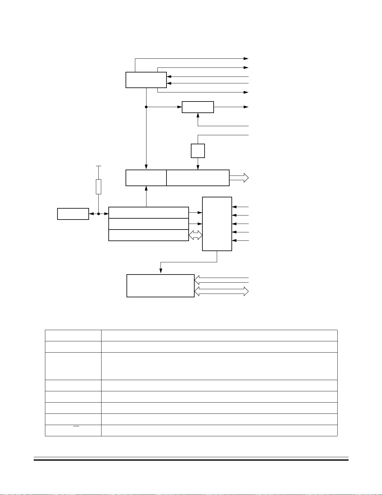
Freescale Semiconductor, Inc.
STOP/WAIT
CONTROL
System Integration Module (SIM)
MODULE STOP
MODULE WAIT
CPU STOP (FROM CPU)
CPU WAIT (FROM CPU)
SIMOSCEN (TO OSCILLATOR)
Introduction
nc...
I
cale Semiconductor,
Frees
INTERNAL
PULL-UP
RESET
PIN LOGIC
VDD
CLOCK
CONTROL
POR CONTROL
RESET PIN CONTROL
SIM RESET STATUS REGISTER
INTERRUPT CONTROL
AND PRIORITY DECODE
CLOCK GENERATORS
COUNTER
RESET
SIM
÷2
MASTER
RESET
CONTROL
COP CLOCK
OSCXCLK (FROM CLOCK DOUBLER)
OSCOUT (FROM CLOCK DOUBLER)
INTERNAL CLOCKS
ILLEGAL OPCODE (FROM CPU)
ILLEGAL ADDRESS (FROM ADDRESS
MAP DECODERS)
COP TIMEOUT (FROM COP MODULE)
LVI RESET (FROM LVI MODULE)
USB RESET (FROM USB MODULE)
INTERRUPT SOURCES
CPU INTERFACE
Figure 8-1. SIM Block Diagram
Table 8-1. SIM Module Signal Name Conventions
Signal Name Description
OSCXCLK Clock doubler output which has twice the frequency of OSC1 from the oscillator
The OSCXCLK frequency divided by two. This signal is again divided by two in the
OSCOUT
IAB Internal address bus
IDB Internal data bus
PORRST Signal from the power-on reset module to the SIM
IRST Internal reset signal
R/W
MC68HC908JB8•MC68HC08JB8•MC68HC08JT8 — Rev. 2.1 Technical Data
MOTOROLA System Integration Module (SIM) 95
SIM to generate the internal bus clocks.
(Bus clock = OSCXCLK ÷ 4 = f
Read/write signal
OSC
÷ 2)
For More Information On This Product,
Go to: www.freescale.com

Freescale Semiconductor, Inc.
System Integration Module (SIM)
Addr.Register Name Bit 7654321Bit 0
Read:
$FE00
Note: Writing a logic 0 clears SBSW.
$FE01
$FE02 Reserved
nc...
I
$FE03
$FE04
Break Status Register
(BSR)
Reset Status Register
(RSR)
Break Flag Control
Register
(BFCR)
Interrupt Status Register 1
(INT1)
Write: See note
Reset: 0
Read: POR PIN COP ILOP ILAD USB LVI 0
Write:
POR:10000000
Read:
Write:
Read:
Write:
Reset: 0
Read: IF6 IF5 IF4 IF3 IF2 IF1 0 0
Write:RRRRRRRR
Reset:00000000
RRRRRR
RRRRRRRR
BCFERRRRRRR
Figure 8-2. SIM I/O Register Summary
8.3 SIM Bus Clock Control and Generation
The bus clock generator provides system clock signals for the CPU and
cale Semiconductor,
peripherals on the MCU. The system clocks are generated from an
incoming clock, OSCOUT, as shown in Figure 8-3.
SBSW
R
Frees
FROM CLOCK
DOUBLER
FROM CLOCK
DOUBLER
OSCXCLK
OSCOUT
SIM COUNTER
÷ 2
SIM
BUS CLOCK
GENERATORS
Figure 8-3. SIM Clock Signals
Technical Data MC68HC908JB8•MC68HC08JB8•MC68HC08JT8 — Rev. 2.1
96 System Integration Module (SIM) MOTOROLA
For More Information On This Product,
Go to: www.freescale.com

Freescale Semiconductor, Inc.
8.3.1 Bus Timing
In user mode, the internal bus frequency is the oscillator frequency
divided by two.
8.3.2 Clock Startup from POR or LVI Reset
When the power-on reset (POR) module or the low-voltage inhibit
module generates a reset, the clocks to the CPU and peripherals are
inactive and held in an inactive phase until after the 4096 OSCXCLK
cycle POR timeout has completed. The RST pin is driven low by the SIM
during this entire period. The IBUS clocks start upon completion of the
nc...
I
timeout.
System Integration Module (SIM)
Reset and System Initialization
cale Semiconductor,
Frees
8.3.3 Clocks in Stop Mode and Wait Mode
Upon exit from stop mode by an interrupt, break, or reset, the SIM allows
OSCXCLK to clock the SIM counter. The CPU and peripheral clocks do
not become active until after the stop delay timeout. This timeout is
selectable as 4096 or 2048 OSCXCLK cycles. (See 8.7.2 Stop Mode.)
In wait mode, the CPU clocks are inactive. The SIM also produces two
sets of clocks for other modules. Refer to the wait mode subsection of
each module to see if the module is active or inactive in wait mode.
Some modules can be programmed to be active in wait mode.
8.4 Reset and System Initialization
The MCU has these reset sources:
• Power-on reset module (POR)
• External reset pin (RST
• Computer operating properly module (COP)
)
• Illegal opcode
• Illegal address
• Universal serial bus module (USB)
• Low-voltage inhibit module (LVI)
MC68HC908JB8•MC68HC08JB8•MC68HC08JT8 — Rev. 2.1 Technical Data
MOTOROLA System Integration Module (SIM) 97
For More Information On This Product,
Go to: www.freescale.com

Freescale Semiconductor, Inc.
System Integration Module (SIM)
All of these resets produce the vector $FFFE–FFFF ($FEFE–FEFF in
monitor mode) and assert the internal reset signal (IRST). IRST causes
all registers to be returned to their default values and all modules to be
returned to their reset states.
An internal reset clears the SIM counter (see 8.5 SIM Counter), but an
external reset does not. Each of the resets sets a corresponding bit in
the reset status register (RSR). (See 8.8 SIM Registers.)
8.4.1 External Pin Reset
nc...
I
cale Semiconductor,
Frees
The RST pin circuit includes an internal pullup device. Pulling the
asynchronous RST pin low halts all processing. The PIN bit of the reset
status register (RSR) is set as long as RST is held low for a minimum of
67 OSCXCLK cycles, assuming that neither the POR nor the LVI was the
source of the reset. See Table 8-2 for details. Figure 8-4 shows the
relative timing.
Reset Type Number of Cycles Required to Set PIN
POR/LVI 4163 (4096 + 64 + 3)
All others 67 (64 + 3)
OSCOUT
RST
IAB
PC
Table 8-2. PIN Bit Set Timing
VECT H VECT L
Figure 8-4. External Reset Timing
Technical Data MC68HC908JB8•MC68HC08JB8•MC68HC08JT8 — Rev. 2.1
98 System Integration Module (SIM) MOTOROLA
For More Information On This Product,
Go to: www.freescale.com

Freescale Semiconductor, Inc.
System Integration Module (SIM)
Reset and System Initialization
8.4.2 Active Resets from Internal Sources
All internal reset sources actively pull the RST pin low for 32 OSCXCLK
cycles to allow resetting of external peripherals. The internal reset signal
IRST continues to be asserted for an additional 32 cycles. (See Figure
8-5.) An internal reset can be caused by an illegal address, illegal
opcode, COP timeout, LVI, the USB module or POR. (See Figure 8-6 .
Sources of Internal Reset.)
NOTE: For LVI or POR resets, the SIM cycles through 4096 OSCXCLK cycles
during which the SIM forces the RST pin low. The internal reset signal
then follows the sequence from the falling edge of RST
nc...
I
Figure 8-5.
shown in
cale Semiconductor,
Frees
IRST
RST
OSCXCLK
IAB
RST PULLED LOW BY MCU
32 CYCLES 32 CYCLES
Figure 8-5. Internal Reset Timing
The COP reset is asynchronous to the bus clock.
ILLEGAL ADDRESS RST
ILLEGAL OPCODE RST
COPRST
POR
LVI
USB
INTERNAL RESET
Figure 8-6. Sources of Internal Reset
VECTOR HIGH
The active reset feature allows the part to issue a reset to peripherals
and other chips within a system built around the MCU.
MC68HC908JB8•MC68HC08JB8•MC68HC08JT8 — Rev. 2.1 Technical Data
MOTOROLA System Integration Module (SIM) 99
For More Information On This Product,
Go to: www.freescale.com

Freescale Semiconductor, Inc.
System Integration Module (SIM)
8.4.2.1 Power-On Reset
When power is first applied to the MCU, the power-on reset module
(POR) generates a pulse to indicate that power-on has occurred. The
external reset pin (RST) is held low while the SIM counter counts out
4096 OSCXCLK cycles. Sixty-four OSCXCLK cycles later, the CPU and
memories are released from reset to allow the reset vector sequence to
occur.
At power-on, the following events occur:
• A POR pulse is generated.
nc...
I
cale Semiconductor,
Frees
• The internal reset signal is asserted.
• The SIM enables the oscillator to drive OSCXCLK.
• Internal clocks to the CPU and modules are held inactive for 4096
OSCXCLK cycles to allow stabilization of the oscillator.
• The RST pin is driven low during the oscillator stabilization time.
• The POR bit of the reset status register (RSR) is set and all other
bits in the register are cleared.
OSC1
PORRST
4096
CYCLES
OSCXCLK
OSCOUT
32
CYCLES
32
CYCLES
RST
IAB
$FFFE $FFFF
Figure 8-7. POR Recovery
Technical Data MC68HC908JB8•MC68HC08JB8•MC68HC08JT8 — Rev. 2.1
100 System Integration Module (SIM) MOTOROLA
For More Information On This Product,
Go to: www.freescale.com
 Loading...