

Datasheet MC68HC711P2CFS4, MC68HC711P2CFN3, MC68HC711P2CFN4, MC68HC11P0CFN3, MC68HC11P1CFN3 Datasheet (Motorola)
...
M68HC11
Microcontrollers
MC68HC11P2
MC68HC711P2
Technical Data
MC68HC11P2/D
Rev. 1, 4/2002
WWW.MOTOROLA.COM/SEMICONDUCTORS


MC68HC11P2
MC68HC711P2
Technical Data — Rev 1.0
Motorola reserves the righ t to make changes without further notice to any products
herein. Motorola makes no warranty, representation or guarantee regarding the
suitability of i ts products for any partic ular purpose, nor does Moto rola assume any
liability arising out of the application or use of any prod uct or circuit, and s pecifically
disclaims any an d all liability, including withou t limitation consequential or inc idental
damages. "Typical" parameters which may be provided in Motorola data sheets and/or
specifications can an d do vary in different applications and actua l performance may
vary over time. A ll operating parameters, i ncluding "Typicals" must be validated for
each customer application by customer’s technical experts. Motorola does not convey
any license under i ts patent rights nor the rig hts of others. Motorola prod ucts are not
designed, intended, or authorized for use as components in systems intended for
surgical implant into the body, or other applications intended to support or sustain life,
or for any other applicat ion in wh ich the failure of the Mo torola pr oduct could cr eate a
situation where personal injury or death may oc cur. Should Buyer purchase o r use
Motorola products for any such unintended or una uthorized application, Buye r shall
indemnify and hold Motorola and its officers, employees, subsid iaries, affiliates, and
distributors harmless against all claims, costs, damages, and expenses, and
reasonable attorney fees arising out of, directly or indirectly, any claim of personal
injury or death associated with such unintended or unauthorized use, even if such claim
alleges that Motorola was negligent reg arding the design o r manufacture of the p art.
Motorola, Inc. is an Equal Opportunity/Affirmative Action Employer.
Motorola and are registered trademarks of Motorola, Inc.
DigitalDNA is a trademark of Motorola, Inc. © Motorola, Inc., 2002
MC68HC11P2 — Rev 1.0 Technical Data
MOTOROLA 3

Technical Data MC68HC11P2 — Rev 1.0
4 MOTOROLA

Technical Data — MC68HC11P2
List of Paragraphs. . . . . . . . . . . . . . . . . . . . . . . . . . . . . . . .5
Table of Contents . . . . . . . . . . . . . . . . . . . . . . . . . . . . . . . .7
List of Figures . . . . . . . . . . . . . . . . . . . . . . . . . . . . . . . . . .13
List of Tables. . . . . . . . . . . . . . . . . . . . . . . . . . . . . . . . . . .15
Section 1. General Description . . . . . . . . . . . . . . . . . . . .17
Section 2. Pin Descriptions . . . . . . . . . . . . . . . . . . . . . . .21
Section 3. Operating Modes and On-Chip Memory . . . .41
Section 4. Parallel In put/Output. . . . . . . . . . . . . . . . . . . .73
Section 5. Serial Communications Interface (SCI). . . . .87
List of Paragraphs
Section 6. Motorola Interconnect Bus (MI BUS). . . . . .109
Section 7. Serial Peripheral Interface (SPI). . . . . . . . . .125
Section 8. Timing System. . . . . . . . . . . . . . . . . . . . . . . .137
Section 9. Analog-to-Digital Converter . . . . . . . . . . . . .173
Section 10. Resets and Interrupts. . . . . . . . . . . . . . . . .185
Section 11. CPU Core and Instruction Set . . . . . . . . . .213
Section 12. Electrical Specificatio ns. . . . . . . . . . . . . . .231
Section 13. Mechanical Data . . . . . . . . . . . . . . . . . . . . .247
Section 14. Ordering Information . . . . . . . . . . . . . . . . .251
Section 15. Development Support. . . . . . . . . . . . . . . . .253
Glossary. . . . . . . . . . . . . . . . . . . . . . . . . . . . . . . . . . . . . .255
MC68HC11P2 — Rev 1.0 Technical Data
MOTOROLA List of Paragraphs 5

List of Paragraphs
Revision History . . . . . . . . . . . . . . . . . . . . . . . . . . . . . . .265
Technical Data MC68HC11P2 — Rev 1.0
6 List of Paragraphs MOTOROLA

Technical Data — MC68HC11P2
1.1 Contents. . . . . . . . . . . . . . . . . . . . . . . . . . . . . . . . . . . . . . . . . .17
Table of Contents
List of Paragraphs
Table of Contents
List of Figures
List of Tables
Section 1. General Description
1.2 Introduction. . . . . . . . . . . . . . . . . . . . . . . . . . . . . . . . . . . . . . . .17
1.3 Features . . . . . . . . . . . . . . . . . . . . . . . . . . . . . . . . . . . . . . . . . .18
Section 2. Pin Descriptions
2.1 Contents. . . . . . . . . . . . . . . . . . . . . . . . . . . . . . . . . . . . . . . . . .21
2.2 Introduction. . . . . . . . . . . . . . . . . . . . . . . . . . . . . . . . . . . . . . . .21
2.3 VDD and VSS. . . . . . . . . . . . . . . . . . . . . . . . . . . . . . . . . . . . . .22
2.4 RESET . . . . . . . . . . . . . . . . . . . . . . . . . . . . . . . . . . . . . . . . . . .23
2.5 Crystal driver and external clock input (XTAL, EXTAL) . . . . . .24
2.6 E clock output (E). . . . . . . . . . . . . . . . . . . . . . . . . . . . . . . . . . .26
2.7 Phase-locked loop (XFC, VDDSYN). . . . . . . . . . . . . . . . . . . . .26
2.8 Interrupt request (IRQ) . . . . . . . . . . . . . . . . . . . . . . . . . . . . . . .32
2.9 Nonmaskable interrupt (XIRQ/VPPE). . . . . . . . . . . . . . . . . . . .32
2.10 MODA and MODB (MODA/LIR and MODB/VSTBY) . . . . . . . .33
MC68HC11P2 — Rev 1.0 Technical Data
MOTOROLA Table of Contents 7

Table of Contents
2.11 VRH and VRL. . . . . . . . . . . . . . . . . . . . . . . . . . . . . . . . . . . . . .34
2.12 PG7/R/W. . . . . . . . . . . . . . . . . . . . . . . . . . . . . . . . . . . . . . . . . .34
2.13 Port signals. . . . . . . . . . . . . . . . . . . . . . . . . . . . . . . . . . . . . . . .34
Section 3. Operating Modes and On-Chip Memory
3.1 Contents. . . . . . . . . . . . . . . . . . . . . . . . . . . . . . . . . . . . . . . . . .41
3.2 Introduction. . . . . . . . . . . . . . . . . . . . . . . . . . . . . . . . . . . . . . . .41
3.3 Operating modes . . . . . . . . . . . . . . . . . . . . . . . . . . . . . . . . . . .41
3.4 On-chip memory. . . . . . . . . . . . . . . . . . . . . . . . . . . . . . . . . . . . 44
3.5 System initialization . . . . . . . . . . . . . . . . . . . . . . . . . . . . . . . . .51
3.6 EPROM, EEPROM and CONFIG register . . . . . . . . . . . . . . . .64
Section 4. Parallel Input/Output
4.1 Contents. . . . . . . . . . . . . . . . . . . . . . . . . . . . . . . . . . . . . . . . . .73
4.2 Introduction. . . . . . . . . . . . . . . . . . . . . . . . . . . . . . . . . . . . . . . .73
4.3 Port A . . . . . . . . . . . . . . . . . . . . . . . . . . . . . . . . . . . . . . . . . . . .74
4.4 Port B . . . . . . . . . . . . . . . . . . . . . . . . . . . . . . . . . . . . . . . . . . . .75
4.5 Port C . . . . . . . . . . . . . . . . . . . . . . . . . . . . . . . . . . . . . . . . . . . .77
4.6 Port D . . . . . . . . . . . . . . . . . . . . . . . . . . . . . . . . . . . . . . . . . . . .78
4.7 Port E . . . . . . . . . . . . . . . . . . . . . . . . . . . . . . . . . . . . . . . . . . . .79
4.8 Port F . . . . . . . . . . . . . . . . . . . . . . . . . . . . . . . . . . . . . . . . . . . .80
4.9 Port G . . . . . . . . . . . . . . . . . . . . . . . . . . . . . . . . . . . . . . . . . . . .81
4.10 Port H . . . . . . . . . . . . . . . . . . . . . . . . . . . . . . . . . . . . . . . . . . . .82
4.11 Internal pull-up/pull-down resistors. . . . . . . . . . . . . . . . . . . . . .83
4.12 System configuration . . . . . . . . . . . . . . . . . . . . . . . . . . . . . . . .84
Technical Data MC68HC11P2 — Rev 1.0
8 Table of Conten ts MOTOROLA

Table of Contents
Section 5. Serial Communications Interface (SCI)
5.1 Contents. . . . . . . . . . . . . . . . . . . . . . . . . . . . . . . . . . . . . . . . . .87
5.2 Introduction. . . . . . . . . . . . . . . . . . . . . . . . . . . . . . . . . . . . . . . .87
5.3 Data format. . . . . . . . . . . . . . . . . . . . . . . . . . . . . . . . . . . . . . . .88
5.4 Transmit operation . . . . . . . . . . . . . . . . . . . . . . . . . . . . . . . . . .89
5.5 Receive operation. . . . . . . . . . . . . . . . . . . . . . . . . . . . . . . . . . .89
5.6 Wakeup feature . . . . . . . . . . . . . . . . . . . . . . . . . . . . . . . . . . . .91
5.7 SCI error detection . . . . . . . . . . . . . . . . . . . . . . . . . . . . . . . . . . 92
5.8 SCI registers. . . . . . . . . . . . . . . . . . . . . . . . . . . . . . . . . . . . . . .93
5.9 Status flags and interrupts . . . . . . . . . . . . . . . . . . . . . . . . . . .101
5.10 Additional SCI subsystems. . . . . . . . . . . . . . . . . . . . . . . . . . .104
Section 6. Motorola Interconnect Bus (MI BUS)
6.1 Contents. . . . . . . . . . . . . . . . . . . . . . . . . . . . . . . . . . . . . . . . .109
6.2 Introduction. . . . . . . . . . . . . . . . . . . . . . . . . . . . . . . . . . . . . . .109
6.3 Push-pull sequence . . . . . . . . . . . . . . . . . . . . . . . . . . . . . . . .111
6.4 The push field. . . . . . . . . . . . . . . . . . . . . . . . . . . . . . . . . . . . .112
6.5 The pull field. . . . . . . . . . . . . . . . . . . . . . . . . . . . . . . . . . . . . .112
6.6 Biphase coding. . . . . . . . . . . . . . . . . . . . . . . . . . . . . . . . . . . .113
6.7 Message validation. . . . . . . . . . . . . . . . . . . . . . . . . . . . . . . . .113
6.8 Interfacing to MI BUS . . . . . . . . . . . . . . . . . . . . . . . . . . . . . . .116
6.9 MI BUS clock rate. . . . . . . . . . . . . . . . . . . . . . . . . . . . . . . . . .117
6.10 SCI/MI BUS2 registers . . . . . . . . . . . . . . . . . . . . . . . . . . . . . .117
6.11 SCI/MI BUS3 registers . . . . . . . . . . . . . . . . . . . . . . . . . . . . . .123
MC68HC11P2 — Rev 1.0 Technical Data
MOTOROLA Table of Contents 9

Table of Contents
Section 7. Serial Peripheral Interface (SPI)
7.1 Contents. . . . . . . . . . . . . . . . . . . . . . . . . . . . . . . . . . . . . . . . .125
7.2 Introduction. . . . . . . . . . . . . . . . . . . . . . . . . . . . . . . . . . . . . . .125
7.3 Functional description. . . . . . . . . . . . . . . . . . . . . . . . . . . . . . .126
7.4 SPI transfer formats . . . . . . . . . . . . . . . . . . . . . . . . . . . . . . . . 1 26
7.5 SPI signals . . . . . . . . . . . . . . . . . . . . . . . . . . . . . . . . . . . . . . .129
7.6 SPI system errors. . . . . . . . . . . . . . . . . . . . . . . . . . . . . . . . . .130
7.7 SPI registers. . . . . . . . . . . . . . . . . . . . . . . . . . . . . . . . . . . . . .132
Section 8. Timing System
8.1 Contents. . . . . . . . . . . . . . . . . . . . . . . . . . . . . . . . . . . . . . . . .137
8.2 Introduction. . . . . . . . . . . . . . . . . . . . . . . . . . . . . . . . . . . . . . .137
8.3 Timer structure . . . . . . . . . . . . . . . . . . . . . . . . . . . . . . . . . . . .139
8.4 Input capture. . . . . . . . . . . . . . . . . . . . . . . . . . . . . . . . . . . . . .142
8.5 Output compare . . . . . . . . . . . . . . . . . . . . . . . . . . . . . . . . . . . 1 45
8.6 Real-time interrupt . . . . . . . . . . . . . . . . . . . . . . . . . . . . . . . . .154
8.7 Computer operating properly watchdog function . . . . . . . . . .157
8.8 Pulse accumulator . . . . . . . . . . . . . . . . . . . . . . . . . . . . . . . . .158
8.9 Pulse-width modulation (PWM) timer . . . . . . . . . . . . . . . . . . .1 62
Section 9. Analog-to-Digital Converter
9.1 Contents. . . . . . . . . . . . . . . . . . . . . . . . . . . . . . . . . . . . . . . . .173
9.2 Introduction. . . . . . . . . . . . . . . . . . . . . . . . . . . . . . . . . . . . . . .173
9.3 Overview. . . . . . . . . . . . . . . . . . . . . . . . . . . . . . . . . . . . . . . . .174
9.4 A/D converter power-up and clock select. . . . . . . . . . . . . . . .178
9.5 Channel assignments. . . . . . . . . . . . . . . . . . . . . . . . . . . . . . . 1 80
9.6 Control, status and results registers. . . . . . . . . . . . . . . . . . . .181
Technical Data MC68HC11P2 — Rev 1.0
10 Table of Contents MOTOROLA

Table of Contents
9.7 Operation in STOP and WAIT modes. . . . . . . . . . . . . . . . . . .184
Section 10. Resets and Interrupts
10.1 Contents. . . . . . . . . . . . . . . . . . . . . . . . . . . . . . . . . . . . . . . . .185
10.2 Introduction. . . . . . . . . . . . . . . . . . . . . . . . . . . . . . . . . . . . . . .185
10.3 Resets. . . . . . . . . . . . . . . . . . . . . . . . . . . . . . . . . . . . . . . . . . .185
10.4 Effects of reset . . . . . . . . . . . . . . . . . . . . . . . . . . . . . . . . . . . .192
10.5 Reset and interrupt priority . . . . . . . . . . . . . . . . . . . . . . . . . . .195
10.6 Interrupts. . . . . . . . . . . . . . . . . . . . . . . . . . . . . . . . . . . . . . . . .200
10.7 Low power operation . . . . . . . . . . . . . . . . . . . . . . . . . . . . . . .203
Section 11. CPU Core and Instruction Set
11.1 Contents. . . . . . . . . . . . . . . . . . . . . . . . . . . . . . . . . . . . . . . . .213
11.2 Introduction. . . . . . . . . . . . . . . . . . . . . . . . . . . . . . . . . . . . . . .213
11.3 Registers. . . . . . . . . . . . . . . . . . . . . . . . . . . . . . . . . . . . . . . . .214
11.4 Data types. . . . . . . . . . . . . . . . . . . . . . . . . . . . . . . . . . . . . . . .220
11.5 Opcodes and operands . . . . . . . . . . . . . . . . . . . . . . . . . . . . .220
11.6 Addressing modes . . . . . . . . . . . . . . . . . . . . . . . . . . . . . . . . .221
11.7 Instruction set. . . . . . . . . . . . . . . . . . . . . . . . . . . . . . . . . . . . .2 23
Section 12. Electrical Specifications
12.1 Contents. . . . . . . . . . . . . . . . . . . . . . . . . . . . . . . . . . . . . . . . .231
12.2 Introduction. . . . . . . . . . . . . . . . . . . . . . . . . . . . . . . . . . . . . . .231
12.3 Maximum ratings . . . . . . . . . . . . . . . . . . . . . . . . . . . . . . . . . .232
12.4 Thermal characteristics and power considerations. . . . . . . . .233
12.5 Test methods . . . . . . . . . . . . . . . . . . . . . . . . . . . . . . . . . . . . .234
12.6 DC electrical characteristics. . . . . . . . . . . . . . . . . . . . . . . . . .235
MC68HC11P2 — Rev 1.0 Technical Data
MOTOROLA Table of Contents 11

Table of Contents
12.7 Control timing . . . . . . . . . . . . . . . . . . . . . . . . . . . . . . . . . . . . .237
Section 13. Mechanical Data
13.1 Contents. . . . . . . . . . . . . . . . . . . . . . . . . . . . . . . . . . . . . . . . .247
13.2 Pin assignments. . . . . . . . . . . . . . . . . . . . . . . . . . . . . . . . . . .248
13.3 Package dimensions. . . . . . . . . . . . . . . . . . . . . . . . . . . . . . . .249
Section 14. Ordering Information
14.1 Contents. . . . . . . . . . . . . . . . . . . . . . . . . . . . . . . . . . . . . . . . .251
14.2 Introduction. . . . . . . . . . . . . . . . . . . . . . . . . . . . . . . . . . . . . . .251
Section 15. Development Support
15.1 Contents. . . . . . . . . . . . . . . . . . . . . . . . . . . . . . . . . . . . . . . . .253
15.2 Introduction. . . . . . . . . . . . . . . . . . . . . . . . . . . . . . . . . . . . . . .253
15.3 EVS — Evaluation system . . . . . . . . . . . . . . . . . . . . . . . . . . .2 53
Glossary
Revision History
15.4 Major Changes Between Revision 1.0 and Revision 0.0 . . . .265
Technical Data MC68HC11P2 — Rev 1.0
12 Table of Contents MOTOROLA

Technical Data — MC68HC11P2
Figure Title Page
1-1 MC68HC11P2/MC68HC711P2 block diagram. . . . . . . . . . . . . 19
2-1 84-pin PLCC/CERQUAD pinout. . . . . . . . . . . . . . . . . . . . . . . .22
2-2 External reset circuitry . . . . . . . . . . . . . . . . . . . . . . . . . . . . . . .24
2-3 Oscillator connections. . . . . . . . . . . . . . . . . . . . . . . . . . . . . . . .25
2-4 PLL circuit. . . . . . . . . . . . . . . . . . . . . . . . . . . . . . . . . . . . . . . . .27
2-5 RAM stand-by connections. . . . . . . . . . . . . . . . . . . . . . . . . . . .33
3-1 MC68HC11P2 memory map. . . . . . . . . . . . . . . . . . . . . . . . . . .44
3-2 RAM and register overlap. . . . . . . . . . . . . . . . . . . . . . . . . . . . .57
5-1 SCI baud rate generator circuit diagram. . . . . . . . . . . . . . . . . .88
5-2 SCI1 block diagram . . . . . . . . . . . . . . . . . . . . . . . . . . . . . . . . .90
5-3 Interrupt source resolution within SCI. . . . . . . . . . . . . . . . . . .1 03
6-1 MI BUS timing. . . . . . . . . . . . . . . . . . . . . . . . . . . . . . . . . . . . .111
6-2 Biphase coding and error detection . . . . . . . . . . . . . . . . . . . .113
6-3 MI BUS block diagram . . . . . . . . . . . . . . . . . . . . . . . . . . . . . .115
6-4 A typical interface between the MC68HC11P2 and the MI BUS
. . . . . . . . . . . . . . . . . . . . . . . . . . . . . . . . . . . . . . . . . . . . . . . .116
7-1 SPI block diagram. . . . . . . . . . . . . . . . . . . . . . . . . . . . . . . . . .127
7-2 SPI transfer format . . . . . . . . . . . . . . . . . . . . . . . . . . . . . . . . .128
8-1 Timer clock divider chains . . . . . . . . . . . . . . . . . . . . . . . . . . .140
8-2 Capture/compare block diagram. . . . . . . . . . . . . . . . . . . . . . .141
8-3 Pulse accumulator block diagram. . . . . . . . . . . . . . . . . . . . . .159
8-4 PWM timer block diagram. . . . . . . . . . . . . . . . . . . . . . . . . . . .164
8-5 PWM duty cycle . . . . . . . . . . . . . . . . . . . . . . . . . . . . . . . . . . .170
9-1 A/D converter block diagram . . . . . . . . . . . . . . . . . . . . . . . . .174
9-2 Electrical model of an A/D input pin (in sample mode). . . . . .175
9-3 A/D conversion sequence. . . . . . . . . . . . . . . . . . . . . . . . . . . .177
10-1 Processing flow out of reset (1 of 2). . . . . . . . . . . . . . . . . . . .206
10-2 Processing flow out of reset (2 of 2). . . . . . . . . . . . . . . . . . . .207
10-3 Interrupt priority resolution (1 of 3) . . . . . . . . . . . . . . . . . . . . .208
List of Figures
MC68HC11P2 — Rev 1.0 Technical Data
MOTOROLA List of Figures 13

List of Figures
10-4 Interrupt priority resolution (2 of 3) . . . . . . . . . . . . . . . . . . . . .209
10-5 Interrupt priority resolution (3 of 3) . . . . . . . . . . . . . . . . . . . . .210
10-6 Interrupt source resolution within the SCI subsystem. . . . . . .211
11-1 Programming model. . . . . . . . . . . . . . . . . . . . . . . . . . . . . . . .214
11-2 Stacking operations . . . . . . . . . . . . . . . . . . . . . . . . . . . . . . . .2 16
12-1 Test methods . . . . . . . . . . . . . . . . . . . . . . . . . . . . . . . . . . . . .2 34
12-2 Timer inputs . . . . . . . . . . . . . . . . . . . . . . . . . . . . . . . . . . . . . .237
12-3 Reset timing . . . . . . . . . . . . . . . . . . . . . . . . . . . . . . . . . . . . . .238
12-4 Interrupt timing . . . . . . . . . . . . . . . . . . . . . . . . . . . . . . . . . . . .238
12-5 STOP recovery timing. . . . . . . . . . . . . . . . . . . . . . . . . . . . . . .239
12-6 WAIT recovery timing. . . . . . . . . . . . . . . . . . . . . . . . . . . . . . .239
12-7 Port read timing diagram . . . . . . . . . . . . . . . . . . . . . . . . . . . .240
12-8 Port write timing diagram . . . . . . . . . . . . . . . . . . . . . . . . . . . .240
12-9 SPI master timing (CPHA = 0) . . . . . . . . . . . . . . . . . . . . . . . .243
12-10 SPI master timing (CPHA = 1) . . . . . . . . . . . . . . . . . . . . . . . .243
12-11 SPI slave timing (CPHA = 0) . . . . . . . . . . . . . . . . . . . . . . . . .244
12-12 SPI slave timing (CPHA = 1) . . . . . . . . . . . . . . . . . . . . . . . . .244
12-13 Expansion bus timing . . . . . . . . . . . . . . . . . . . . . . . . . . . . . . .246
13-1 84-pin PLCC/CERQUAD pinout. . . . . . . . . . . . . . . . . . . . . . .248
13-2 84-pin PLCC mechanical dimensions. . . . . . . . . . . . . . . . . . .249
13-3 84-pin CERQUAD mechanical dimensions . . . . . . . . . . . . . .250
Technical Data MC68HC11P2 — Rev 1.0
14 List of Figures MOTOROLA

Technical Data — MC68HC11P2
Table Title Page
2-1 Port signal functions. . . . . . . . . . . . . . . . . . . . . . . . . . . . . . . . .35
3-1 Example bootloader baud rates . . . . . . . . . . . . . . . . . . . . . . . .43
3-2 Register and control bit assignments . . . . . . . . . . . . . . . . . . . .47
3-3 Registers with limited write access. . . . . . . . . . . . . . . . . . . . . .51
3-4 Hardware mode select summary . . . . . . . . . . . . . . . . . . . . . . .53
3-5 RAM and register remapping . . . . . . . . . . . . . . . . . . . . . . . . . .56
3-6 EEPROM remapping . . . . . . . . . . . . . . . . . . . . . . . . . . . . . . . .58
3-7 EEPROM block protect. . . . . . . . . . . . . . . . . . . . . . . . . . . . . . .62
3-8 Erase mode selection. . . . . . . . . . . . . . . . . . . . . . . . . . . . . . . .67
4-1 Port configuration . . . . . . . . . . . . . . . . . . . . . . . . . . . . . . . . . . .74
5-1 Example SCI baud rate control values . . . . . . . . . . . . . . . . . . .95
7-1 SPI clock rates . . . . . . . . . . . . . . . . . . . . . . . . . . . . . . . . . . . .1 33
8-1 Timer resolution and capacity. . . . . . . . . . . . . . . . . . . . . . . . .139
8-2 RTI periodic rates. . . . . . . . . . . . . . . . . . . . . . . . . . . . . . . . . .154
8-3 Pulse accumulator timing . . . . . . . . . . . . . . . . . . . . . . . . . . . .158
8-4 Clock A and clock B prescalers . . . . . . . . . . . . . . . . . . . . . . .167
9-1 A/D converter channel assignments. . . . . . . . . . . . . . . . . . . .180
10-1 COP timer rate select. . . . . . . . . . . . . . . . . . . . . . . . . . . . . . .187
10-2 Reset cause, reset vector and operating mode . . . . . . . . . . .192
10-3 Highest priority interrupt selection . . . . . . . . . . . . . . . . . . . . .198
10-4 Interrupt and reset vector assignments . . . . . . . . . . . . . . . . .199
10-5 Stacking order on entry to interrupts. . . . . . . . . . . . . . . . . . . .201
11-1 Reset vector comparison . . . . . . . . . . . . . . . . . . . . . . . . . . . .217
11-2 Instruction set. . . . . . . . . . . . . . . . . . . . . . . . . . . . . . . . . . . . .223
14-1 Ordering information. . . . . . . . . . . . . . . . . . . . . . . . . . . . . . . .251
15-1 M68HC11 development tools . . . . . . . . . . . . . . . . . . . . . . . . .253
List of Tables
MC68HC11P2 — Rev 1.0 Technical Data
MOTOROLA List of Tables 15

List of Tables
Technical Data MC68HC11P2 — Rev 1.0
16 List of Tables MOTOROLA

Technical Data — MC68HC11P2
1.1 Contents
1.2 Introduction. . . . . . . . . . . . . . . . . . . . . . . . . . . . . . . . . . . . . . .17
1.3 Features. . . . . . . . . . . . . . . . . . . . . . . . . . . . . . . . . . . . . . . . . .18
1.2 Introduction
The MC68HC11P2 8-bit microcomputer is a member of the M68HC11
family of HCMOS microco mput ers. In additi on to 32kbytes of ROM, the
MC68HC11P2 cont ains 1kbyte of RAM and 640 bytes of EEPROM. With
its advanced timer and communication features (including MI BUS
the MC68HC11P2 is especially suitable for mobile communications and
automotive applications.
Section 1. General Description
(1)
)
The MC68HC711P2 is an EPROM version of the MC68HC11P2, with
the User ROM replaced by a similar amount of EPROM. All references
to the MC68HC11P2 apply equally to the MC68HC711P2, unless
otherwise noted. References specific to the MC68HC711P2 are
italicised in the text.
1. The Motorola interconnect bus (MI BUS) is a serial communications protocol which supports
distributed real-tim e control effi ciently and with a high degr ee of noise immunity. I t allows data
to be transferred between the MCU and the slave de vice using only one wire, making this ty pe
of communication suitable for medium speed networks requiring very low cost multiplex wiring.
MC68HC11P2 — Rev 1.0 Technical Data
MOTOROLA General Description 17

General Description
1.3 Features
• Low power, high performanc e M68HC11 CPU core, with 4MHz
bus capability
• Power saving PLL clock circuit, with automatic disable during
WAIT mode
• 32kbytes of User ROM (MC68HC11P2); 32kbytes User EPROM
(MC68HC711P2)
• 1kbyte of RAM
• 640 bytes of byte-erasable User EEPROM, with on-chip charge
pump
• Up to 50 general purpose I/O lines, plus up to 12 input-only lines
• Non-multiplexed addr ess and data buses, permitting dir ect access
to the full 64k address map
• 16-bit timer with 3/4 input captures and 4/5 output compares;
pulse accumulator and COP watchdog timer
• Three 8- or 9-bit SCI subsystems, two with MI BUS† capability
• SPI subsystem, with software selectable MSB/LSB first option
• 8-channel, 8-bit analog-to-digital (A/D) converter
• Four 8-bit PWM timer channels (may be concatenated to form
one, or two, 16-bit channels)
• Available in 84-pin PLCC or 84-pin CERQUAD packages
Technical Data MC68HC11P2 — Rev 1.0
18 General Description MOTOROLA
General Description
Features
VPPE/XIRQ
IRQ
RESET
LIR/MODA
VSTBY/MODB
XTAL
EXTAL
XFC
VDDSYN
VDD
VSS
ROM or EPROM
Pulse accumula to r
Timer
Periodic inte rr u pt
COP watchdog
OC1/PAI
OC1/OC2
OC1/OC3
OC1/OC4
IC4/OC1/OC5
IC1
IC2
IC3
PA7
PA6
PA5
PA4
PA3
Port APort D
PA2
PA1
PA0
32768 x 8
(including 64 bytes for vectors)
SPI
SCI1+
640 bytes EEPROM
8-channel
A/D
converter
1024 bytes RAM
Interrupts
SS
SCK
MOSI
MISO
TXD1
RXD1
AD7
AD6
AD5
AD4
AD3
AD2
AD1
AD0
R/W
&
mode
select
E
Oscillator
PLL
5
5
M68HC11
CPU
SCI3+ (with MI BUS)
SCI2+ (with MI BUS)
PWM
TXD3
RXD3
TXD2
RXD2
PW4
PW3
PW2
PW1
PD5
PD4
PD3
PD2
PD1
PD0
VRH
VRL
PE7
PE6
PE5
PE4
PE3
Port E
PE2
PE1
PE0
PG7
PG6
PG5
PG4
PG3
Port G
PG2
PG1
PG0
PH7
PH6
PH5
PH4
PH3
Port H
PH2
PH1
PH0
Non-multiplexed address and data buses
A15
A14
A13
A12
A11
A10A9A8
A7A6A5A4A3A2A1A0D7D6D5D4D3D2D1
D0
Port B Port F Port C
PF6
PF5
PF4
PF3
PF2
PF1
PF0
PC7
PC6
PC5
PC4
PC3
PC2
PC1
PB7
PB6
PB5
PB4
PB3
PB2
PB1
PB0
PF7
PC0
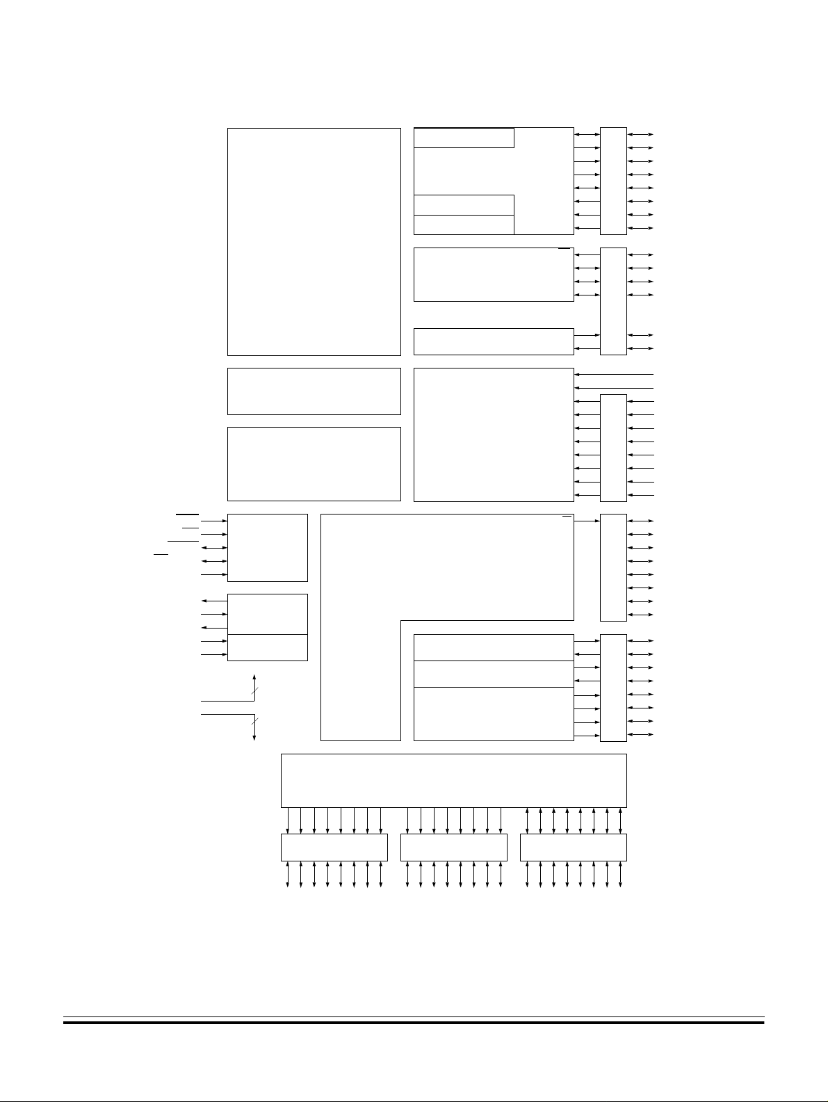
Figure 1-1. MC68HC11P2/MC68HC711P2 block diagram
MC68HC11P2 — Rev 1.0 Technical Data
MOTOROLA General Description 19

General Description
Technical Data MC68HC11P2 — Rev 1.0
20 General Description MOTOROLA

Technical Data — MC68HC11P2
2.1 Contents
2.2 Introduction. . . . . . . . . . . . . . . . . . . . . . . . . . . . . . . . . . . . . . .21
2.3 VDD and VSS. . . . . . . . . . . . . . . . . . . . . . . . . . . . . . . . . . . . . .22
2.4 RESET . . . . . . . . . . . . . . . . . . . . . . . . . . . . . . . . . . . . . . . . . . .23
2.5 Crystal driver and external clock input (XTAL, EXTAL) . . .24
2.6 E clock output (E). . . . . . . . . . . . . . . . . . . . . . . . . . . . . . . . . .26
2.7 Phase-locked loop (XFC, VDDSYN) . . . . . . . . . . . . . . . . . . .26
2.8 Interrupt request (IRQ). . . . . . . . . . . . . . . . . . . . . . . . . . . . . .32
2.9 Nonmaskable interrupt (XIRQ/VPPE) . . . . . . . . . . . . . . . . . .32
Section 2. Pin Descriptions
2.2 Introduction
2.10 MODA and MODB (MODA/LIR and MODB/VSTBY) . . . . . . .33
2.11 VRH and VRL. . . . . . . . . . . . . . . . . . . . . . . . . . . . . . . . . . . . . .34
2.12 PG7/R/W. . . . . . . . . . . . . . . . . . . . . . . . . . . . . . . . . . . . . . . . . .34
2.13 Port signals. . . . . . . . . . . . . . . . . . . . . . . . . . . . . . . . . . . . . . .34
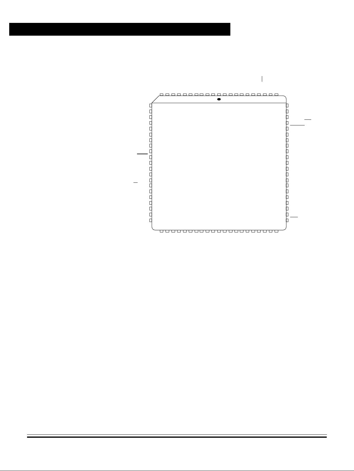
The MC68HC11P2 is available in an 84-pin plastic-leaded chip carrier
(PLCC); the MC68HC711P2 is also available in an 84-pin windowed
cerquad package, to all ow full use of the EPROM. Most pins on this MCU
serve two or more functions, as described in the following paragraphs.
Refer to Figure 2-1 which shows the pin assignments for both 84-pin
packages.
MC68HC11P2 — Rev 1.0 Technical Data
MOTOROLA Pin Descriptions 21
Pin Descriptions
PW1/PH0
PW2/PH1
PW3/PH2
PW4/PH3
RXD2/PH4
TXD2/PH5
RXD3/PH6
TXD3/PH7
MODB/VSTBY
R/W
XIRQ
VDD
VDDL
VSSX
VSS
/PG7
PG6
PG5
PG4
PG3
PG2
PG1
PB0/A8
PB1/A9
PB2/A10
PB3/A11
PB4/A12
PB5/A13
PB6/A14
PB7/A15
VSS
VDD
PA0/IC3
PA1/IC2
PA2/IC1
PA3/OC1/OC5/IC4
PA4/OC1/OC4
PA5/OC1/OC3
PA6/OC1/OC2
65432
987
11
10
12
13
14
15
16
17
18
19
20
21
22
23
24
25
26
27
28
29
30
31
32
333435363738394041424344454647484950515253
8483828180
7978777675
PA7/OC1/PAI
PD5/SS
PD4/SCK
PD3/MOSI
74
PD2/MISO
73
PD1/TXD1
72
PD0/RXD1
71
MODA/LIR
RESET
70
XFC
69
VDDSYN
68
EXTAL
67
XTAL
66
E
65
VDDR
64
VSSX
63
PC7/D7
62
PC6/D6
61
PC5/D5
60
PC4/D4
59
PC3/D3
58
PC2/D2
57
PC1/D1
56
PC0/D0
55
IRQ
54
2.3 VDD and VSS
PG0
VDD AD
AD7/PE7
AD6/PE6
AD5/PE5
AD4/PE4
AD3/PE3
VRL
VRH
A7/PF7
A6/PF6
A5/PF5
A4/PF4
A3/PF3
A2/PF2
A1/PF1
AD2/PE2
AD1/PE1
VSS AD
AD0/PE0
A0/PF0
Figure 2-1. 84-pin PLCC/CERQUAD pinout
Power is supplied to the microcontroller via these pins. VDD is the
positive supply and VSS is grou nd. The MCU op erates from a single 5V
(nominal) power supply.
It is in the nature of CMOS designs that very fast signal transitions occur
on the MCU pins. These short rise and fall times place very high shortduration current demands on the power supply. To prevent noise
problems, special care must be taken to provide good power supply
bypassing at the MCU. Bypass capacitors should have good highfrequency characteristics and be as close to the MCU as possible.
Technical Data MC68HC11P2 — Rev 1.0
22 Pin Descriptions MOTOROLA

2.4 RESET
Pin Descriptions
RESET
Bypassing requirem e nts v ar y, depending on how heavily the MCU p ins
are loaded.
The MC68HC11P2 MCU has five VDD pins and five VSS pins. One pair
of these pins is reserved for supplying power to the analog-to-digital
converter (VDD AD, VSS AD); two pairs are used for the internal logic
(VDD, VSS); the remaining two pairs supply power for the port logic on
either half of the chip (VDDL, VSSX and VDDR, VSSX). This
arrangement minimizes the injection of noise into the digital circuitry on
the chip.
An active low bidirectional control signal, RESET, acts as an input to
initialize the MCU to a known start- up state. It also acts as an open-drain
output to indicate that an internal failure has been detected in either the
clock monitor or the COP watchdog circuit. The CPU distinguishes
between internal and external reset conditions by sensing whether the
reset pin rises to a logic one in less than six E clock cycles after a reset
has occurred. It is therefore not advisable to connect an external
resistor-capacitor (RC) power-up delay circuit to the reset pin of
M68HC11 devices because the circuit charge time constant can cause
the device to misinterpret the type of reset that occurred. Refer to
Resets and Interrupts for further information.
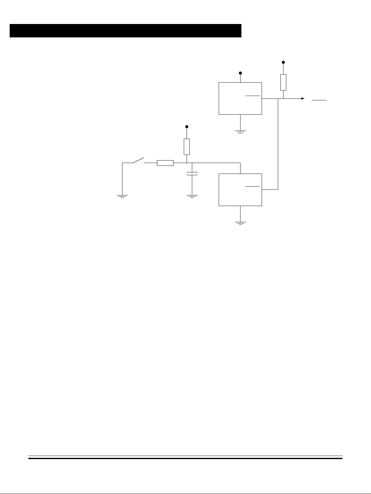
Figure 2-2 illustrates a typical reset circuit that includes an external
switch together with a low voltage inhibit circuit, to prevent power
transitions, or RAM or EEPROM corruption.
MC68HC11P2 — Rev 1.0 Technical Data
MOTOROLA Pin Descriptions 23
Pin Descriptions
V
V
DD
DD
Manual
reset
4.7 k¾
2
IN
1
GND
IN
GND
RESET
3
2
RESET
3
1
MC34064
V
DD
4.7 k¾
1µF
MC34164
4.7 k¾
To M68HC11
RESET
Figure 2-2. External reset circuitry
2.5 Crystal driver and external clock input (XTAL, EXTAL)
These two pins provide the interface for either a cr ystal or a CMOS
compatible clock to control the internal clock generator circuitry. The
frequency applied to these pins must be four times higher than the
desired E clock rate (unless the PLL circuit is used to provide the E
clock).
The XTAL pin is normally left unconnected when an external CMOS
compatible clock inp ut is connected to the EXTAL pin. However , a 10 k¾
to 100 k¾ load resistor connected from XTAL to ground can be used to
reduce RFI noise emission. The XTAL output is normally intended to
drive only a crys tal. The XTAL output can be buffered with a highimpedance buffe r, o r i t can be u sed to dri ve the EX TAL inp ut of a nothe r
M68HC11 family device.
Technical Data MC68HC11P2 — Rev 1.0
24 Pin Descriptions MOTOROLA
Pin Descriptions
Crystal driver and external clock input (XTAL, EXTAL)
In all cases, use caution when designing circuitry associated with the
oscillator pins. Load cap acitances shown in the oscillator cir cuits include
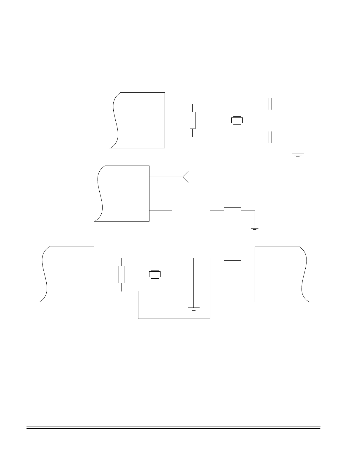
all stray layout capacitances. See Figure 2-3.
(a) Common crystal
connections
(b) External oscilla tor
connections
EXTAL
M68HC11
M68HC11
EXTAL
XTAL
EXTAL
XTAL
10 M¾
External oscillator
NC or
10–100k¾ load
25 pF
25 pF
4•E
crystal
25 pF
220¾
EXTAL
M68HC11
XTAL
(c) One crystal driving two MCUs
10 M¾
4•E
crystal
25 pF
M68HC11
NC or
10–100k¾
load
Note: capacitor values include all stray capacitance.
XTAL
Figure 2-3. Oscillator connections
MC68HC11P2 — Rev 1.0 Technical Data
MOTOROLA Pin Descriptions 25

Pin Descriptions
2.6 E clock output (E)
E is the output connect ion for the internally generated E clo ck. The signal
from E is used as a timing reference. The frequency of the E clock output
is one quarter that of the input frequency at the XTAL and EXTAL pins
(except when the PLL is used as the clock source). When E clock outp ut
is low, an internal process is taking place; when it is high, data is being
accessed. All clocks, including the E clock, are halted when the MCU is
in STOP mode. The E clock output can be turned off in single chip
modes to reduce the effects of RFI.
2.7 Phase-locked loop (XFC, VDDSYN)
The XFC and VDDSYN pins are the inputs for the on-chip PLL (phaselocked loop) circuitry. On rese t all the device clocks are de rived from the
EXTAL input. The EXTAL clock is used as a reference for the PLL circuit,
which generates a cl ock that is a multiple of the EXTAL frequency. Once
the PLL has stabilized, alternate clocks may be selected.
VDDSYN is the powe r supply pin for the PL L. Connecting it high en ables
the internal low frequency oscillator circuitry designed for the PLL. The
PLL has been designed particularly for use with 614.4 and 640kHz
crystals, though other values may be used. The maximum
recommended crystal freq uency for PLL opera tion is 2MHz. Above this
frequency VDDSYN sh ould be g roun ded to disa ble the PLL a nd en able
the high frequency oscillator circuit; in this state EXTAL is designed for
16MHz operation and XFC may be left unconnected.
The PLL consists of a variable bandwidth loop filter, a voltage controlled
oscillator (VCO), a feedback frequency divider and a digital phase
detector. VDDSYN is the supply voltage for th e PLL and must be suitab ly
bypassed. The extern al capacito r on XFC sh ould be located a s close to
the chip as possible to minimi ze nois e. A typical val ue for thi s capacito r
is 0.047µF, for a crystal frequency of 614.4kHz.
1. In general, a larger capacitor will improve the PLL’s frequency stability, at the expense of increasing the time required for it to settle (t
cation, or one in which the slew rate is not critical, a capacitor value of 0.1µF is usually
adequate. For a crystal frequency of 614.4kHz and a slew time of 1–2ms (from 614kHz in
WAIT mode to 16MHz in RUN mode), a capacitor of 0.047µF has been found satisfactory.
Technical Data MC68HC11P2 — Rev 1.0
26 Pin Descriptions MOTOROLA
) at the desired frequency. For a 32kHz appli-
PLLS
(1)

Pin Descriptions
Phase-locked loop (XFC, VDDSYN)
The PLL filter has two band widths that are au tomatically selected by th e
PLL, if the AUTO bit in PLL CR is set. Whenever the PLL is first enable d,
the wide bandwidth mode is used. This enables the PLL frequency to
ramp up quickly. When the output frequency is near the desired value,
the filter is switched to the narrow bandwidth mode, to make the final
frequency more stable. Manual control is possible, by clearing AUTO in
PLLCR, and setting the appropriate value for BWC.
A block diagram of the PLL circuitry is given in Figure 2-4.
V
DDSYN
EXTAL
t
REF
EXTAL
Low frequency
crystal oscillator
Phase
detect
PCOMP
t
FB
XFC
Loop filter VCO
Frequency divider
SYNR
VCOOUT
Figure 2-4. PLL circuit
4XCLK
Bus clock
select
To clock
generation
circuitry
BCS
ST4XCK
Module clock
select
For SCI
and timer
EXTAL
MCS
2.7.1 Synchronization of PLL with subsystems
The timer and SCI subsystems operate off the EXTAL clock, but are
accessed by the CPU relative to the internal PH2 signal. Although the
EXTAL clock is used as the referenc e for the PLL, the PH2 clock and the
module clocks for the timer and the SCI are not synchronized. In order
to ensure synchronized data , special circuitry has been incorporated into
both subsystems.
MC68HC11P2 — Rev 1.0 Technical Data
MOTOROLA Pin Descriptions 27

Pin Descriptions
2.7.2 Changing the PLL frequency
To change the PLL frequency it is necessary to perform the following
sequence of events, in order to prevent possible bursts of high frequency
operation during the reconfiguration of the PLL:
1. Switch to the low frequency bus rate (BCS = 0)
2. Disable the PLL (PLLON = 0)
3. Change the value in SYNR
4. Enable the PLL (PLLON = 1)
5. Wait a time t
6. Switch to the high frequency bus rate (BCS = 1)
2.7.3 PLL registers
Two registers are used to control the operation of the MC68HC11P2
phase-locked loop circuitry. These are the PLL control register and the
synthesizer program register, each of which is described below.
2.7.3.1 PLLCR — PLL control register
Address bit 7 bit 6 bit 5 bit 4 bit 3 bit 2 bit 1 bit 0
PLL control (PLLCR) $002E PLLON BCS AUTO BWC VCOT MCS LCK WEN 1010 1000
This read/write register contains two bits that are used to enable and
disable the synthesizer and to switch from slow (EXTAL) to one of the
fast speeds. Two further bi ts are used to control the filt er bandwidth. The
SCI and timer clock source and the slow clock for WAIT mode are also
controlled by this register.
for the PLL frequency to stabilize
PLLS
State
on reset
PLLON — PLL on
1 = Switch PLL on.
0 = Switch PLL off.
Technical Data MC68HC11P2 — Rev 1.0
28 Pin Descriptions MOTOROLA

Pin Descriptions
Phase-locked loop (XFC, VDDSYN)
This bit activates the synthesizer circuit without connecting it to the
control circuit. This allows the circuit to stabilize before it drives the
CPU clocks. PLLON is set by reset, to allow the control loop to
stabilize during power up.
PLLON cannot be cleared whilst using VCOOUT to drive the internal
processor clock, i.e. when BCS is set.
BCS — Bus clock select
1 = VCOOUT output drives the clock circuit (4XCLK).
0 = EXTAL drives t he clock circuit (4XCLK).
This bit determine s which signal drives the clock cir cuit generating the
bus clocks. Once BCS has been altered it can take up to [1.5 EX TAL
+ 1.5 VCOOUT] cycles for the change in the clock to occur. Reset
clears this bit.
NOTE: PLLON and BCS have built-in safeguards so that VCOOUT cannot be
selected as the clock source (BCS = 1) if the PLL is off (PLLON = 0).
Similarly, the PLL ca nnot be tu rned off ( PLLON = 0) if it is on and in us e
(BCS = 1). Turning th e PLL on and selecting VCOOUT as the clock
source therefore requires two independent writes to PLLCR.
AUTO — Automatic bandwidth control
1 = Automatic bandwidth control selected.
0 = Manual bandwidth control selected.
AUTO selects between automatic bandwidth control circuits in the
phase detect block and manual bandwidth control. Reset sets this bit.
BWC — Bandwidth control
1 = High bandwidth control selected.
0 = Low bandwidth control selected.
Bandwidth control is unde r manu al cont rol onl y when AU TO is clear.
(When AUTO is set, BWC acts as a read-only status bit to indicate
which mode has been selected by the internal circuit.) A delay of t
is required between changes to BWC. The low bandwidth driver is
always enabled, so this bit determines whether the high bandwidth
driver is on or off. On PLL start-up in automatic mode (AUTO = 1), th e
high bandwidth driver is enabled (BWC = 1) by internal circuitry until
PLLS
MC68HC11P2 — Rev 1.0 Technical Data
MOTOROLA Pin Descriptions 29

Pin Descriptions
the PLL is near the specif ied frequ ency. The high bandwidth driver is
then disabled and BWC is cleared by internal circuitry. Reset clears
this bit.
Auto BWC
00 Off
01 On
1XAuto
High
bandwidth
VCOT — VCO test (Test mode only)
1 = Loop filter operates as specified by AUTO and BWC.
0 = Low bandwidth mode of the PLL filter is disabled .
This bit is used to isolate the loop filter from the VCO for testing
purposes. VCOT is always set when AUTO = 1 when running in
automatic mode. This bit is writable only in test mode. Reset sets this
bit.
MCS — Module clock select
1 = 4XCLK is the source for the SCI and timer divider chain.
0 = EXTAL is the source for the SCI and timer divider chain.
Reset clears this bit.
LCK — Synthesizer lock detect
1 = The PLL has stabilized.
0 = The PLL is not stable.
This bit is used as an indicator for software that it is all right to set
BCS.
WEN — WAIT enable
1 = Low-power WAIT mode selected (PLL set to ‘idle’ in WAIT
mode).
0 = Do not alter the 4XCLK during WAIT mode.
This bit determines whether the 4XCLK is disconnected from
VCOOUT during WAIT and connected to EXTAL. Reset clears this
bit.
When set, the CPU will respond to a WAIT instruction by first stacking
the relevant registers, then by clearing BCS and setting the PLL to
‘idle’, with modulus = 1.
Technical Data MC68HC11P2 — Rev 1.0
30 Pin Descriptions MOTOROLA

Any interrupt, any reset, or the assertion of RAF in any of the SCIs will
allow the PLL to resume operating at the frequency specified in the
SYNR. The user must set BCS after the PLL has had time to adjust
(t
). If, for a specific SCI, the RE bit is clear, then RAF cannot
PLLS
become set, hence the PLL will not resume normal operation.
2.7.3.2 SYNR — Synthesizer program register
Pin Descriptions
Phase-locked loop (XFC, VDDSYN)
Addressbit 7bit 6bit 5bit 4bit 3bit 2bit 1bit 0
Synthesizer program (SYNR) $002F SYNX1SYNX0SYNY5SYNY4SYNY3SYNY2SYNY1SYNY00000 1011
State
on reset
The PLL frequency synthesizer multiplies the frequency of the crystal
oscillator. The mult ipl ication factor is softw are pro gramm able vi a a loop
divider, which c onsists of a six-bit modulo N counter, with a further two
bit scaling factor.
The multiplicatio n factor is given by 2(Y + 1)2X, where 0 ð X ð 3 and 0 ð
Y ð 63.
NOTE: Exceeding recommended operating frequencies can result in
indeterminate MCU operation.
SYNX[1:0]
These bits program the binary taps (divide by 1, 2, 4 and 8). Reset
clears these bits.
SYNY[5:0]
These bits program the six-bit modulo N (1 to 64) counter. Reset sets
these bits to %001011.
NOTE: The resolut ion of the multiplic ation facto rs decreases b y a fa ctor of two,
as X increases:
X Y Possible multipliers
00 – 63 2, 4, 6, 8, …, 128
10 – 63 4, 8, 12, 16, …, 256
20 – 63 8, 16, 24, 32, …, 512
30 – 63 16, 32, 48, 64, …, 1024
MC68HC11P2 — Rev 1.0 Technical Data
MOTOROLA Pin Descriptions 31

Pin Descriptions
2.8 Interrupt request (IRQ)
The IRQ input provides a means of applying asynchronous interrupt
requests to the MCU. Either falling edge sensitive triggering or level
sensitive triggering is program selectable (OPTION register). IRQ is
always configured to level sensitive triggering at reset.
NOTE: Connect an external pull-up resistor, typically 4.7k¾, to V
is used in a level sensitive wired-OR configuration. See also
Nonmaskable interrupt (XIRQ/VPPE).
2.9 Nonmaskable interrupt (XIRQ/VPPE)
The XIRQ input provides a means of requesting a non-maskable
interrupt after reset initialization. During reset, the X bit in the condition
code register (CCR) is set and any interrupt is masked until MCU
software enables it. B ecause the X IRQ input is level-sensitive, it can be
connected to a multiple-source wired- OR network with an external pullup resistor to VDD. XIRQ is often used as a power loss detect interrupt.
Whenever XIRQ or IRQ is used with multip le interrupt sources (IRQ
must be configured for level sensitive operation if there is more than one
source of IRQ interrupt), each source must drive the interrupt input with
an open-drain type of driver t o avoid con tention betw een outputs. There
should be a single pull-up resistor near the MCU interrupt input pin
(typical ly 4. 7 k¾). There must also be an interlock mechanism at each
interrupt source so that the source holds the interrupt line low until the
MCU recognizes and ackn owledges the interrupt req uest. If one or more
interrupt source is still pending after the MCU services a re quest, the
interrupt line will still be held low and the MCU will be interrupted again
as soon as the interrupt mask bit in the MCU is cleared (normally upon
return from an interrupt). Refer to Resets and Interrupts.
when IRQ
DD
The VPPE pin is used to input the external EPROM programming
voltage, which must be present during EPROM programming.
Technical Data MC68HC11P2 — Rev 1.0
32 Pin Descriptions MOTOROLA

MODA and MODB (MODA/LIR and MODB/VSTBY)
2.10 MODA and MODB (MODA/LIR and MODB/VSTBY)
During reset, MODA and MODB sele ct one of the fo ur operatin g modes.
Refer to Operating Modes and On-Chip Memory.
After the operating mode has been selected, the LIR pin provides an
open-drain output to indicate that executi on of an instruction has begun.
The LIR pin is normally configured for wired-OR operation (only pulls
low). In order to detect consecutive instructions in a high-speed
application, this signal can be made to drive high for a short time to
prevent false triggering. A series of E clock cycles occurs during
execution of each instruction. The LIR signal goes low during the first E
clock cycle of each instruction (opcod e fetch). This output is provided for
assistance in program debugging and its operation is controlled by the
LIRDV bit in the OPT2 register.
Pin Descriptions
The VSTBY pin is used to input RAM stand-by power. The MCU is
powered from the VDD pin unless the difference between the level of
VSTBY and VDD is greater than one MOS threshold (about 0.7 volts).
When these voltages differ by more than 0.7 volts, the internal 1024-byte
RAM and part of the reset logic are powered from VSTBY rather than
VDD. This allows RAM contents to be retained without VDD power
applied to the MCU. Reset must be driven low before VDD is removed
and must remain low until VDD has been restored to a valid level.
V
DD
4.8 V NiCd
(+)
V
DD
MAX 690
V
BATT
V
OUT
4.7k¾
To MODB/VSTBY
pin of M68HC1 1
Figure 2-5. RAM stand-by connections
MC68HC11P2 — Rev 1.0 Technical Data
MOTOROLA Pin Descriptions 33

Pin Descriptions
2.11 VRH and VRL
2.12 PG7/R/W
These pins provide the reference voltages for the analog-to-digital
converter.
This pin provides two separate functions, depending on the operating
mode. In single chip and bootstr ap mo de s, PG7/R /W acts as
input/output port G bit 7. Refer to Parallel Input/Output for further
information.
In expanded and test m odes, PG7/R/W performs the read/writ e function.
PG7/R/W signals the direction of transfers on the external data bus. A
high on this pin indicates that a read cycle is in progress.
2.13 Port signals
NOTE: When using the information about port functions, do not confuse pin
In the 84-pin PLCC package , 62 pins are arranged into seven 8-bit ports:
A, B, C, E, F, G, and H, and on e six- bit port ( D). The lines of ports A, B,
C, D, F, G, and H are fully bidirectional; E is input only. Each of the
bidirectional ports serves a purpose other than I/O, depending on the
operating mode or p eri ph er al fun cti on se le cte d. N ote t hat ports B, C, F,
and one bit of port G are available for I/O functions only in single chip
and bootstrap modes. Refer to Table 2-1 for details of the port signals’
functions in different operating modes.
function with the electrical state of the pin at reset. All general-purpose
I/O pins configure d as inputs at reset are in a high-impedance state. P ort
data registers reflect the functional state of the port at reset. The pin
function is mode dependent.
Technical Data MC68HC11P2 — Rev 1.0
34 Pin Descriptions MOTOROLA

Table 2-1. Port signal functions
Pin Descriptions
Port signals
Single chip
Port/bit
PA0 PA0/IC3
PA1 PA1/IC2
PA2 PA2/IC1
PA3 PA3/OC5/IC4 and/or OC1
PA4 PA4/OC4 and/or OC1
PA5 PA5/OC3 and/or OC1
PA6 PA6/OC2 and/or OC1
PA7 PA7/PAI and/or OC1
PB[7:0] PB[7:0] A[15:8]
PC[7:0] PC[7:0] D[7:0]
PD0 PD0/RXD1
PD1 PD1/TXD1
PD2 PD2/MISO
PD3 PD3/MOSI
PD4 PD4/SCK
PD5 PD5/SS
PE[7:0] Input only or analog inputs
PF[7:0] PF[7:0] A[7:0]
PG[6:0] PG[6:0]
PG7 PG7/R/W
PH0 PH0/PW1
PH1 PH1/PW2
PH2 PH2/PW3
PH3 PH3/PW4
PH4 PH4/RXD2
PH5 PH5/TXD2
PH6 PH6/RXD3
PH7 PH7/TXD3
and
bootstrap mode
Expanded multiplexed
and
special test mode
2.13.1 Port A
Port A is an 8-bit general- purpose I/O port w ith a data regist er (PORTA)
and a data direction register (DDRA). Port A pins share functions with
the 16-bit timer system (see Timing System for further information).
PORTA can be read at any time: inputs return the pin level; outputs
return the pin driver input level. If written, PORTA stores the data in
internal latches. The pins are driven only if they are configured as
MC68HC11P2 — Rev 1.0 Technical Data
MOTOROLA Pin Descriptions 35

Pin Descriptions
2.13.2 Port B
outputs. Writes to PORTA do not change the pin state wh en the pins are
configured for timer output compares.
Out of reset, port A pins [7:0] are general-purpose high-impedance
inputs. When the function s associa ted wi th the se pin s are disab led, the
bits in DDRA govern the I/O state of the associated pin. For further
information, refer to Parallel Input/Output.
Port B is an 8-bit general- purpose I/O port w ith a data regist er (PORTB)
and a data direction re gister (DDRB). In single chip mode, por t B pins are
general-purpose I/O pins (PB[7:0]). In expanded mode, port B pins act
as the high-order address lines (A[15:8]) of the address bus.
PORTB can be read at any time: inputs return the pin level; outputs
return the pin dr iver inpu t level. If POR TB is writ ten, the data i s stored in
internal latches. The pins are driven only if they are configured as
outputs in single chip or b ootstrap mode. For further information, refer to
Parallel Input/Output.
2.13.3 Port C
Port B pins include on-chip pull-up devices which can be enabled or
disabled.
Port C is an 8 -bit general -purpose I/O port with a data regi ster (PORTC)
and a data direction register (DDRC). In single chip mode, port C pins
are general-purpose I/O pins (PC[7:0]). In the expanded mode, port C
pins are configured as data bus pins (D[7:0]).
PORTC can be read at any time: inputs return the pin level; outputs
return the pin driver i nput level . If PORTC is writt en, the d ata is store d in
internal latches. The pins are driven only if they are configured as
outputs in single chip or bootstrap mode. Port C pins are generalpurpose inputs out of reset in single chip and bootstrap modes. In
expanded and test modes, these pins are data bus lines out of reset.
Technical Data MC68HC11P2 — Rev 1.0
36 Pin Descriptions MOTOROLA

2.13.4 Port D
Pin Descriptions
Port signals
The CWOM control bit in the OPT2 register disables port C’s P-channel
output drivers. Be cau se the N-ch annel dr iver is no t affecte d by C WOM,
setting CWOM causes port C to become an open -drain- type output port
suitable for wired-OR oper ation. In wired -OR mode (PORTC bits at logic
level zero), the pins are actively dr i ven lo w by the N-chan ne l dr i ver .
When a port C bit is at logic level one, the associated pin is in a high
impedance state as neither the N-channel nor the P-channel devices are
active. It is customary to have an external pull-up resistor on lines that
are driven by open-drain devices. Port C can only be configured for
wired-OR operation when the MCU is in single chip mode. For further
information, refer to Parallel Input/Output.
Port D, a 6-bit g eneral-purpose I/O port, has a data register (PORTD)
and a data direction register (DDRD). The six p ort D lines (D[5:0]) can
be used for general-purpose I/O, for one of the serial communications
interfaces (SCI1, bits [0:1]) and for the serial peripheral interface (SPI,
bits [2:5]) subsystem.
2.13.5 Port E
PORTD can be read at any time: inputs return the pin level; outputs
return the pin driver i nput level . If PORTD is writt en, the d ata is store d in
internal latches and are driven only if port D is configured for generalpurpose output.
For further information, refer to Parallel Input/Output, Serial
Communications Interface (SCI) and Serial Peripheral Interface
(SPI).
Port E, PE/AD[7:0], is an input-only port that can also be used as the
analog inputs for the analog-to-digital converter.
For further information, refer to Parallel Input/Output and Analog-to-
Digital Converter.
MC68HC11P2 — Rev 1.0 Technical Data
MOTOROLA Pin Descriptions 37

Pin Descriptions
2.13.6 Port F
Port F is an 8-bit general-purpose I/O port with a data register (P ORTF)
and a data direction register (DDRF). In single chip mode, port F pins are
general-purpose I/O pins (PF[7:0]). In expanded mode, port F pins act
as the low-order address lines (A[7:0]) of the address bus.
PORTF can be read at any time: inputs return the pin level; outputs
return the pin driver input level. If PORTF is written, the data is stored in
internal latches. The pins are driven only if they are configured as
outputs in single chip or bootstrap mode.
Port F pins include on-chip pull-up devices that can be enabled or
disabled.
For further information, refer to Parallel Input/Output.
2.13.7 Port G
2.13.8 Port H
In normal modes, Port G is a n 8-bit general-purpose I/O port with a data
register (PORTG) and a data direction register (DDRG). Port G bit 7 is
the R/W line in expanded mode; the remaining bits are always general
purpose I/O.
PORTG can be read at any time: inputs return the pin level; outputs
return the pin driver input level. If PORTG is written, the data is stored in
internal latches.The pins are driven only if they are configured as outputs
in single chip or bootstrap mode. For further information, refer to Parallel
Input/Output.
Port G pins include on-chip pull-up devices that can be enabled or
disabled.
Port H is an 8 -bit general -purpose I/O port with a data regi ster (PORTH)
and a data direction register (DDRH). Port H pins support either
input/output, SCI2 (bits [7:6]), SCI3 (bits [5:4]), or pulse-width
modulation channels (bits [3:0]). Both of these SCI subsystems also
have MI BUS capability.
Technical Data MC68HC11P2 — Rev 1.0
38 Pin Descriptions MOTOROLA

Pin Descriptions
Port signals
PORTH can be read at any time: inputs return the pin level; outputs
return the pin driver i nput level . If PORTH is writt en, the d ata is store d in
internal latches. The pins are driven only if they are configured as
outputs in single chip or bootstrap mode.
Port H pins includ e on-chip pull-up or pull-down de vices that can be
enabled or disabled via the Port pull-up assignment register (PPAR).
Port H [7:4] have pull-up resistors; p ort H [3 :0] h ave pull-do wn resistors.
For further information, refer to Parallel Input/Output, Serial
Communications Interface (SCI), Motorola Interconnect Bus
(MI BUS) and Timing System.
MC68HC11P2 — Rev 1.0 Technical Data
MOTOROLA Pin Descriptions 39

Pin Descriptions
Technical Data MC68HC11P2 — Rev 1.0
40 Pin Descriptions MOTOROLA

Technical Data — MC68HC11P2
Section 3. Operating Modes and On-Chip Memory
3.1 Contents
3.2 Introduction. . . . . . . . . . . . . . . . . . . . . . . . . . . . . . . . . . . . . . .41
3.3 Operating modes . . . . . . . . . . . . . . . . . . . . . . . . . . . . . . . . . .41
3.4 On-chip memory . . . . . . . . . . . . . . . . . . . . . . . . . . . . . . . . . . .44
3.5 System initialization. . . . . . . . . . . . . . . . . . . . . . . . . . . . . . . .51
3.6 EPROM, EEPROM and CONFIG register . . . . . . . . . . . . . . .64
3.2 Introduction
This section contains information about the modes that define
MC68HC11P2 op erating conditions , and about the on-chi p memory that
allows the MCU to be configur ed for var i ou s appl ic ati o ns.
3.3 Operating modes
The values of the mode select inputs MODB and MODA during reset
determine the ope rating mode. Single chi p and expanded modes are the
normal modes. In single chip mode only on-board memory is available.
Expanded mode, however, allows access to external memory. Each of
these two normal modes is paired with a special mode. Bootstrap, a
variation of the single chip mode, is a special mode that executes a
bootloader program in an internal bootstrap ROM. Test is a special
mode that allows privileged access to internal resources.
MC68HC11P2 — Rev 1.0 Technical Data
MOTOROLA Operating Modes and On-Chip Memory 41

Operating Modes and On-Chip Memory
3.3.1 Single chip operating mode
In single chip ope rating mode, the MC68HC11P2 microc ontroller has no
external address or data bus. Ports B, C, F, and the R/W pin are
available for general-purpose parallel I/O.
3.3.2 Expanded operating mode
In expanded operating mode, the MCU can access a 64kbyte physical
address space. The address space includes the same on-chip me m or y
addresses used for single chip mode, in add ition to external memo ry and
peripheral devices.
The expansion bus is made up of ports B, C, and F, and the R/W signal.
In expanded mode, hig h order address bits are o utput on the port B pins,
low order address bits on t he port F pins, and the data bus on port C. Th e
R/W/PG7 pin signals the direction of data transfer on the port C bus.
3.3.3 Special test mode
Special test, a variatio n of the expa nd ed mode, i s primar ily us ed duri ng
Motorola’s internal production testing; however, it is accessible for
programming the CO NFIG register, programming calibration data into
EEPROM, and supporting emulation and debugging during
development.
Technical Data MC68HC11P2 — Rev 1.0
42 Operating Modes and On-Chip Memory MOTOROLA

3.3.4 Special bootstrap mode
When the MCU is reset in special bootstrap mode, a small on-chip ROM
is enabled at address $BE 40–$BFFF. The ROM conta ins a reset vector
and a bootloader program. The MCU fetches the reset vector, then
executes the bootloader.
For normal use of the bootloader program, send a synchronization byte
$FF to the SCI receiver at either E clock ÷25 6, or E clo ck ÷1664 (7812
or 1200 baud respectively, for an E clock of 2MHz). Then download up
to 1024 bytes of progr am data (which is p ut into RAM star ting at $0080).
These characters are echoed through the transmitter. The bootloader
program ends the download after a timeout of four character times or
1024 bytes. When loading is complete, the program jumps to location
$0080 and begins exec uting the code. Use of an external pull-up resistor
is required when using the SCI transmitter pin (TXD) because port D pins
are configured for wired-OR op eration by the bootloader. In bootstrap
mode, the interrupt vectors point to RAM. This allows the use of
interrupts through a jump table.
Operating Modes and On-Chip Memory
Operating modes
Further baud rate op tions are available on the MC68HC11P2 by using a
different value for the synchro nization byte, as shown in Table 3-1. Refer
also to Motorola appl ic at ion note AN1060, M68HC11 Bootstrap Mode
(the bootloader mode is similar to that used on the MC68HC11K4).
Table 3-1. Example bootloader baud rates
Sync.
byte
$FF 4 char. 7812 8192 11718 12288 15624
$FF 4 1200 1260 1800 1890 2400
$F0 4.9 9600 10080 14400 15120 19200
$FD 17.3 5208 5461 7812 8192 10416
$FD 13 3906 4096 5859 6144 7812
Timeout
delay
2.00MHz 2.10MHz 3.00MHz 3.15MHz 4.00MHz
Baud rates for an E clock of:
MC68HC11P2 — Rev 1.0 Technical Data
MOTOROLA Operating Modes and On-Chip Memory 43

Operating Modes and On-Chip Memory
3.4 On-chip memory
The MC68HC11P2 M CU includes 1024 bytes of on-chip RAM, 32kbytes
of ROM/EPROM and 640 bytes of EEPROM. The bootloader ROM
occupies a 512 byte block of the memory map. The CONFIG register is
implemented as a separate EEPROM byte.
Start
address
$0000
$0080
$0480
$0D80
$1000
$8000
$BE40
$C000
$FFC0
–$FFFF
Single
chip
Expanded Special
Bootstrap
Special
Test
Register
block
RAM
1024 bytes
EEPROM
640 bytes
BootROM
Vectors
NVM
32kbytes
Vectors
$x000
$x07F
$x080
$x47F
$xD80
$xFFF
$BE40
$BFFF
$8000
$FFBF
$FFFF
Each of these blocks
can be mapped to any
4k page boundary,
using the INIT register.
This block may be remapped
to any 4k page, using INIT2.
Special Bootstrap mode only.
Special modes only.
32kbytes ROM
(MC68H C 11P2) or
32kbytes EPROM
(MC68HC711P2).
Can be mapped to either
$0000–$7FFF or
$8000–$FFFF,
using the CONFIG register.
Normal mode vectors.
Figure 3-1. MC68HC11P2 memory map
3.4.1 Mapping allocations
Memory locations for on-chi p resources are the same for both expanded
and single chip modes. The 12 8-byte regi ster blo ck origi nates at $0000
after reset and can be placed at any other 4k boundary ($x000) after
reset by writing an app ropriate value to the IN IT register. Refer to Figure
3-1, which shows the memory map.
The on-board 1024-b yte RAM is initially located at $0080 aft er reset. The
RAM is divided into two sections of 128 byt es and 896 bytes. If RAM and
Technical Data MC68HC11P2 — Rev 1.0
44 Operating Modes and On-Chip Memory MOTOROLA

Operating Modes and On-Chip Memory
On-chip memory
registers are both mapped to the same 4k boundary, RAM starts at
$x080 and 128 bytes are remapped at $x400–$x47F. Otherwise, RAM
starts at $x00 0.
Remapping is accomplished by writing appropriate values into the two
nibbles of the INIT register.
The 640-byte EEPROM is initially located at $0D80 after reset when
EEPROM is enabled in the memory map by the CONFIG register.
EEPROM can be placed at any ot her 4k bounda ry ($xD80) by writi ng to
the INIT2 register.
If ROM is available, the ROMAD and ROMON bits in the CONFIG
register control the position and presence of ROM in the memory map.
In special test mode, the ROMON bit is cleared so the ROM is removed
from the memory map. In single chip mode, the ROMAD bit is set to one
after reset, which enables the ROM at $8000–$FFFF. In expanded
mode, the ROM may be enabled from $0000–7FFF (ROMAD = 0) to
allow an external memory to contain the interrupt vectors and
initialization code.
In special bootstrap mode, a bootloader ROM is enabled at locations
$BE40–$BFFF. The vectors for special bootstrap mode are contained in
the bootloader progr am. The boot ROM occupies a 512 by te block of the
memory map, though not all locations are used.
3.4.1.1 RAM
The MC68HC11P2 ha s 10 24 b y te s of f ul ly stat ic R A M t hat are used for
storing instructions, variables and temporary data during program
execution. RAM can be placed at any 4k boundary in the 64kbyte
address space by writing an appropriate value to the INIT register.
By default, RAM is initially located at $0080 in the memory map. Direct
addressing mode can acce ss the first 128 location s of RAM using a onebyte address op erand. Direct mode accesses save program memory
space and execution time. R egisters c an be mo ved to oth er bounda ries
to allow 256 bytes of RAM to be located in direct addressing space.
MC68HC11P2 — Rev 1.0 Technical Data
MOTOROLA Operating Modes and On-Chip Memory 45

Operating Modes and On-Chip Memory
The on-chip RAM is a fully static memory. RAM contents can be
preserved during periods of processor inactivity by either of two
methods, both of which reduce power consumption:
1. During the software-based STOP mode, MCU clocks are stop ped,
but the MCU continues to draw power from VDD. Power supply
current is directly related to operating frequency in CMOS
integrated circuits and there is very little leakage when the clocks
are stopped. Thes e two factors reduce power consumptio n while
the MCU is in STOP mode.
2. To reduce power consumption to a minimum, VDD can be turned
off, and the MODB/VSTBY p in can be used to supply RAM power
from either a battery back-up or a second power supply. Although
this method requires external hardware, it is very effective. Refer
to Pin Descriptions for information about how to connect the
stand-by RAM power supply and to Resets and Interrupts for a
description of low power operation.
3.4.1.2 ROM and EPROM
3.4.1.3 Bootloader ROM
The MC68HC11P2 MCU has 32kbytes of ROM/EPROM. The
ROM/EPROM array is enabled when the ROMON bit in the CONFIG
register is set to one (erased). The ROMAD bit in CONFIG places the
ROM/EPROM at either $8000–$FFFF out of reset (ROMAD = 1) or at
$0000–$7FFF (ROMAD = 0) in expanded mode.
The bootloader ROM is enabled at address $BE40–$BFFF during
special bootstrap mode. The reset vector is fetched from this ROM an d
the MCU executes the bootloader firmware. In normal modes, the
bootloader ROM is disabled.
Technical Data MC68HC11P2 — Rev 1.0
46 Operating Modes and On-Chip Memory MOTOROLA

3.4.2 Registers
Table 3-2. Register and control bit assignments (Sheet 1 of 4)
Operating Modes and On-Chip Memory
On-chip memory
In Table 3-2, a summary of registers and control bits, the registers are
shown in ascending order within the 128-byte register block. The
addresses shown are for default block mapping ($0000–$007F),
however, the INIT register remaps the block to any 4k page
($x000–$x07F).
Register name
Port A data (PORTA) $0000 PA7 PA6 PA5 PA4 PA3 PA2 PA1 PA0 undefined
Data direction A (DDRA) $0001 DDA7 DDA6 DDA5 DDA4 DDA3 DDA2 DDA1 DDA0 0000 0000
Data direction B (DDRB) $0002 DDB7 DDB6 DDB5 DDB4 DDB3 DDB2 DDB1 DDB0 0000 0000
Data direction F (DDRF) $0003 DDF7 DDF6 DDF5 DDF4 DDF3 DDF2 DDF1 DDF0 0000 0000
Port B data (PORTB) $0004 PB7 PB6 PB5 PB4 PB3 PB2 PB1 PB0 undefined
Port F data (PORTF) $0005 PF7 PF6 PF5 PF4 PF3 PF2 PF1 PF0 undefined
Port C data (PORTC) $0006 PC7 PC6 PC5 PC4 PC3 PC2 PC1 PC0 undefined
Data direction C (DDRC) $0007 DDC7 DDC6 DDC5 DDC4 DDC3 DDC2 DDC1 DDC0 0000 0000
Port D data (PORTD) $0008 0 0 PD5 PD4 PD3 PD2 PD1 PD0 undefined
Data direction D (DDRD) $0009 0 0 DDD5 DDD4 DDD3 DDD2 DDD1 DDD0 0000 0000
Port E data (PORTE) $000A PE7 PE6 PE5 PE4 PE3 PE2 PE1 PE0 undefined
Timer compare force (CFORC) $000B FOC1 FOC2 FOC3 FOC4 FOC5 0 0 0 0000 0000
Output compare 1 mask (OC1M) $000C OC1M7 OC1M6 OC1M5 OC1M4 OC1M3 0 0 0 0000 0000
Output compare 1 data (OC1D) $000D OC1D7 OC1D6 OC1D5 OC1D4 OC1D3 0 0 0 0000 0000
Timer count (TCNT) high $000E (bit 15) (14) (13) (12) (11) (10) (9) (bit 8) 0000 0000
Timer count (TCNT) low $000F (bit 7) (6) (5) (4) (3) (2) (1) (bit 0) 0000 0000
Timer input capture 1 (TIC1) high $0010 (bit 15) (14) (13) (12) (11) (10) (9) (bit 8) undefined
Timer input capture 1 (TIC1) low $0011 (bit 7) (6) (5) (4) (3) (2) (1) (bit 0) undefined
Timer input capture 2 (TIC2) high $0012 (bit 15) (14) (13) (12) (11) (10) (9) (bit 8) undefined
Timer input capture 2 (TIC2) low $0013 (bit 7) (6) (5) (4) (3) (2) (1) (bit 0) undefined
Timer input capture 3 (TIC3) high $0014 (bit 15) (14) (13) (12) (11) (10) (9) (bit 8) undefined
Timer input capture 3 (TIC3) low $0015 (bit 7) (6) (5) (4) (3) (2) (1) (bit 0) undefined
Timer output compare 1 (TOC1) high $001 6 (bit 15) (14) (13) (12) (11) (10) (9) (bit 8) 1111 1111
Timer output compare 1 (TOC1) low $0017 (bit 7) (6) (5) (4) (3) (2) (1) (bit 0) 1111 1111
Timer output compare 2 (TOC2) high $001 8 (bit 15) (14) (13) (12) (11) (10) (9) (bit 8) 1111 1111
Timer output compare 2 (TOC2) low $0019 (bit 7) (6) (5) (4) (3) (2) (1) (bit 0) 1111 1111
Timer output compare 3 (TOC3) high $001A (bit 15) (14) (13) (12) (11) (10) (9) (bit 8) 1111 1111
Timer output compare 3 (TOC3) low $001B (bit 7) (6) (5) (4) (3) (2) (1) (bit 0) 1111 1111
Address
bit 7 bit 6 bit 5 bit 4 bit 3 bit 2 bit 1 bit 0
State
on reset
MC68HC11P2 — Rev 1.0 Technical Data
MOTOROLA Operating Modes and On-Chip Memory 47

Operating Modes and On-Chip Memory
Table 3-2. Register and control bit assignments (Sheet 2 of 4)
Register name
Timer output compare 4 (TOC4) high $001C (bit 15) (14) (13) (12) (11) (10) (9) (bit 8) 1111 1111
Timer output compare 4 (TOC4) low $ 001D (bit 7) (6) (5) (4) (3) (2) (1) (b it 0) 1111 1111
Capture 4/compare 5 (TI4/O5) high $001E (bit 15) (14) (13) (12) (11) (10) (9) (bit 8) 1111 1111
Capture 4/compare 5 (TI4/O5) low $001F (bit 7) (6) (5) (4) (3) (2) (1) (bit 0) 1111 1111
Timer control 1 (TCTL1) $0020 OM2 OL2 OM3 OL3 OM4 OL4 OM5 OL5 0000 0000
Timer control 2 (TCTL2) $0021 EDG4B EDG4A EDG1B EDG1A EDG2B EDG2A EDG3B EDG3A 0000 0000
Timer interrupt mask 1 (TMSK1) $0022 OC1I OC2I OC3I OC4I I4/O5I IC1I IC2I IC3I 0000 0000
Timer interrupt flag 1 (TFLG1) $0023 OC1F OC2F OC3F OC4F I4/O5F IC1F IC2F IC3F 0000 0000
Timer interrupt mask 2 (TMSK2) $0024 TOI RTII PAOVI PAII 0 0 PR1 PR0 0000 0000
Timer interrupt flag 2 (TFLG2) $0025 TOF RTIF PAOVF PAIF 0 0 0 0 0000 0000
Pulse accumulator control (PACTL) $0026 0 PAEN PAMODPEDGE 0 I4/O5 RTR1 RTR0 0000 0000
Pulse accumulator count (PACNT) $0027 (bit 7) (6) (5) (4) (3) (2) (1) (bit 0) undefined
SPI control (SPCR) $0028 SPIE SPE DWOM MSTR CPOL CPHA SPR1 SPR0 0000 01uu
SPI status (SPSR) $0029 SPIF WCOL 0 MODF 0 0 0 0 0000 0000
SPI data (SPDR) $002A (bit 7) (6) (5) (4) (3) (2) (1) (bit 0) undefined
EPROM programming (EPROG)
Port pull-up assignment (PPAR) $002C 0 0 0 0 HPPUE GPPUE FPPUE BPPUE 0000 1111
reserved $002D
PLL control (PLLCR) $002E PLLON BCS AUTO BWC VCOT MCS LCK WEN 1010 1000
Synthesizer program (SYNR) $002F SYNX1 SYNX0 SYNY5 SYNY4 SYNY3 SYNY2 SYNY1 SYNY0 0000 1011
A/D control & status (ADCTL) $0030 CCF 0 SCAN MULT CD CC CB CA u0uu uuuu
A/D result 1 (ADR1) $0031 (bit 7) (6) (5) (4) (3) (2) (1) (bit 0) undefined
A/D result 2 (ADR2) $0032 (bit 7) (6) (5) (4) (3) (2) (1) (bit 0) undefined
A/D result 3 (ADR3) $0033 (bit 7) (6) (5) (4) (3) (2) (1) (bit 0) undefined
A/D result 4 (ADR4) $0034 (bit 7) (6) (5) (4) (3) (2) (1) (bit 0) undefined
B lock protect (BPROT) $0035 BULKP 0 BPRT4 PTCON BPRT3 BPRT2 BPRT 1 BPRT0 1011 1111
reserved $0036
EEPROM mapping (INIT2) $0037 EE3 EE2 EE1 EE0 M3DL1 M3DL0 M2DL1 M2DL0 0000 0000
System config. options 2 (OPT2) $0038 LIRDV CWOM STRCH IRVNE LSBF SPR2 0 0 000x 0000
System config. options 1 (OPTION) $0039 ADPU CSEL IRQE DLY CME FCME CR1 CR0 0001 0000
COP timer arm/reset (COPRST) $003A (bit 7) (6) (5) (4) (3) (2) (1) (bit 0) undefined
EEPROM programming (PPROG) $003B ODD EVEN 0 BYTE ROW ERASE EELAT EEPGM 0000 0000
Highest priority interrupt (HPRIO) $003C RBOOT SMOD MDA PSEL4 PSEL3 PSEL2 PSEL1 PSEL0 xxx0 0110
RAM & I/O mapping (INIT) $003D RAM3 RAM2 RAM1 RAM0 REG3 REG2 REG1 REG0 0000 0000
Factory test (TEST1) $003E TILOP PLTST OCCR CBYP DISR FCM FCOP MIDLY 0000 x000
Configuration control (CONFIG ) $003F ROMAD 1 1 PAREN NOSECNOC OPRO MON EEON x1 1x 1xxx
Address
‡
$002B MBE 0 ELAT EXCOL EXROW 0 0 EPGM 0000 0000
bit 7 bit 6 bit 5 bit 4 bit 3 bit 2 bit 1 bit 0
State
on reset
Technical Data MC68HC11P2 — Rev 1.0
48 Operating Modes and On-Chip Memory MOTOROLA

Operating Modes and On-Chip Memory
Table 3-2. Register and control bit assignments (Sheet 3 of 4)
On-chip memory
Register name
reserved $0040
reserved $0041
reserved $0042
reserved $0043
reserved $0044
reserved $0045
reserved $0046
reserved $0047
reserved $0048
reserved $0049
reserved $004A
reserved $004B
reserved $004C
reserved $004D
reserved $004E
reserved $004F
SCI/MI 2/3 baud high (S2BDH) $0050 B2TST B2SPL 0 S2B12 S2B11 S2B10 S2B9 S2B8 0000 0000
SCI/MI 2/3 baud low (S2BDL) $0051 S2B7 S2B6 S2B5 S2B4 S2B3 S2B2 S2B1 S2B0 0000 0100
SCI/MI 2 control 1 (S2CR1) $0052 LOPS2 WOMS2 MIE2 M2 WAKE2 ILT2 PE2 PT2 0000 0000
SCI/MI 2 control 2 (S2CR2) $0053 TIE2 TCIE2 RIE2 ILIE2 TE2 RE2 RWU2 SBK2 0000 0000
SCI/MI 2 status 1 (S2SR1) $0054 TDRE2 TC2 RDRF2 IDLE2 OR2 NF2 FE2 PF2 1100 0000
SCI/MI 2 status 2 (S2SR2) $0055 0 0 0 0 0 0 0 RAF2 0000 0000
SCI/MI 2 data high (S2DRH) $0056 R8B T 8B 0 0 0 0 0 0 undefined
SCI/MI 2 data low (S2DRL) $0057 R7T7B R6T6B R5T5B R4T4B R3T3B R2T2B R1T1B R0T0B undefined
reserved $0058
reserved $0059
SCI/MI 3 control 1 (S3CR1) $005A LOPS3 WOMS3 MIE3 M3 WAKE3 ILT3 PE3 PT3 0000 0000
SCI/MI 3 control 2 (S3CR2) $005B TIE3 TCIE3 RIE3 ILIE3 TE3 RE3 RWU3 SBK3 0000 0000
SCI/MI 3 status 1 (S3SR1) $005C TDRE3 TC3 RDRF3 IDLE3 OR3 NF3 FE3 PF3 1100 0000
SCI/MI 3 status 2 (S3SR2) $005D 0 0 0 0 0 0 0 RAF3 0000 0000
SCI/MI 3 data high (S3DRH) $005E R8C T8C 0 0 0 0 0 0 undefined
SCI/MI 3 data low (S3DRL) $005F R7T7C R6T6C R5T5C R4T4C R3T3C R2T2C R1T1C R0T0C undefined
Pulse width clock select (PWCLK) $0060 CON34 CON12 PCKA2 PCKA1 0 PCKB3 PCKB2 PCKB1 0000 0000
Pulse width polarity select (PWPOL) $0061 PCLK4 PCLK3 PCLK2 PCLK1 PPOL4 PPOL3 PPOL2 PPOL1 0000 0000
Pulse width scale (PWSCAL) $0062 (bit 7) (6) (5) (4) (3) (2) (1) (bit 0) 0000 0000
Pulse width enable (PWEN) $0063 TPWSL DISCP 0 0 PWEN4PWEN3 PWEN2PWEN1 0000 0000
Pulse width count 1 (PWCNT1) $0064 (bit 7) (6) (5) (4) (3) (2) (1) (bit 0) 0000 0000
Address
bit 7 bit 6 bit 5 bit 4 bit 3 bit 2 bit 1 bit 0
State
on reset
MC68HC11P2 — Rev 1.0 Technical Data
MOTOROLA Operating Modes and On-Chip Memory 49

Operating Modes and On-Chip Memory
Table 3-2. Register and control bit assignments (Sheet 4 of 4)
Register name
Pulse width count 2 (PWCNT2) $0065 (bit 7) (6) (5) (4) (3) (2) (1) (bit 0) 0000 0000
Pulse width count 3 (PWCNT3) $0066 (bit 7) (6) (5) (4) (3) (2) (1) (bit 0) 0000 0000
Pulse width count 4 (PWCNT4) $0067 (bit 7) (6) (5) (4) (3) (2) (1) (bit 0) 0000 0000
P ulse width period 1 (PWPER1) $0068 (bit 7) (6) (5) (4) (3) (2) (1) (bit 0) 1111 1111
P ulse width period 2 (PWPER2) $0069 (bit 7) (6) (5) (4) (3) (2) (1) (bit 0) 1111 1111
P ulse width period 3 (PWPER3) $006A (bit 7) (6) ( 5) (4) (3) (2) (1) (bit 0) 1111 1111
P ulse width period 4 (PWPER4) $006B (bit 7) (6) ( 5) (4) (3) (2) (1) (bit 0) 1111 1111
P ulse width duty 1 (PWDTY1) $006C (bit 7) (6) (5) (4) (3) (2) (1) (bit 0) 1111 1111
P ulse width duty 2 (PWDTY2) $006D (bit 7) (6) (5) (4) (3) (2) (1) (bit 0) 1111 1111
P ulse width duty 3 (PWDTY3) $006E (bit 7) (6) (5) (4) (3) (2) (1) (bit 0) 1111 1111
P ulse width duty 4 (PWDTY4) $006F (bit 7) (6) (5) (4) (3) (2) (1) (bit 0) 1111 1111
SCI 1 baud rate high (SCBDH) $0070 BTST BSPL 0 SBR12 SBR11 SBR10 SBR9 SBR8 0000 0000
SCI 1 baud rate low (SCBDL) $0071 SBR7 SBR6 SBR5 SBR4 SBR3 SBR2 SBR1 SBR0 0000 0100
SCI 1 control 1 (SCCR1) $0072 LOOPS WOMS 0 M WAKE ILT PE PT 0000 0000
SCI 1 control 2 (SCCR2) $0073 TIE TCIE RIE ILIE TE RE RWU SBK 0000 0000
SCI 1 status 1 (SCSR1) $0074 TDRE TC RDRF IDLE OR NF FE PF 1100 0000
SCI 1 status 2 (SCSR2) $0075 0 0 0 0 0 0 0 RAF 0000 0000
SCI 1 data high (SCDRH) $0076 R8 T8 0 0 0 0 0 0 undefined
SCI 1 data low (SCDRL) $0077 R7T7 R6T6 R5T5 R4T4 R3T3 R2T2 R1T1 R0T0 undefined
reserved $0078
reserved $0079
reserved $007A
reserved $007B
Port H data (PORTH) $007C PH7 PH6 PH5 PH4 PH3 PH2 PH1 PH0 undefined
Data direction H (DDRH) $007D DDH7 DDH6 DDH5 DDH4 DDH3 DDH2 DDH1 DDH0 0000 0000
Port G data (PORTG) $007E PG7 PG6 PG5 PG4 PG3 PG2 PG1 PG0 undefined
Data direction G (DDRG) $007F DDG7 DDG6 DDG5 DDG4 DDG3 DDG2 DDG1 DDG0 0000 0000
Address
bit 7 bit 6 bit 5 bit 4 bit 3 bit 2 bit 1 bit 0
State
on reset
KEY
‡
Applies only to EPROM devices
x State on reset depends on mode selected
u State of bit on reset is undefined
Technical Data MC68HC11P2 — Rev 1.0
50 Operating Modes and On-Chip Memory MOTOROLA

3.5 System initialization
Registers and bi ts that control init ialization and the basic operation o f the
MCU are protected against writes except under special circumstances.
The following table lists registers that can be written only once after
reset, or that must be written within the first 64 cycles after reset.
Table 3-3. Registers with limited write access
Operating Modes and On-Chip Memory
System initialization
Register
address
$x024 Timer interrupt mask register 2 (TMSK2)
$x035 Block protect register (BPROT)
$x037 EEPROM mapping register (INIT2) No Yes
$x038 System configuration options regis ter 2 (OPT2) No
$x039 System configuration options register (OPTION)
$x03D RAM and I/O map register (INIT) Yes —
1. Bits 1 and 0 can be written once and only in first 64 cycles; when SMOD = 1, however, these bits can be written at any
time. All other bits can be written at any time.
2. Bits can be written to zero once and only in first 64 cycles or in special modes. Bits can be set to one at any time.
3. Bit 4 (IRVNE) can be written only once.
4. Bits 5, 4, 2, 1, and 0 can be written once and only in first 64 cycles; when SMOD = 1, however, bits 5, 4, 2, 1, and 0 can
be written at any time. All other bits can be written at any time.
Register
name
Must be written in
first 64 cycles
(1)
(2)
(4)
Write
once only
—
—
(3)
—
3.5.1 Mode selection
The four mode variations ar e selected by the lo gic states of th e mode A
(MODA) and mode B (MODB ) pins during reset. The MO DA and MODB
logic levels determine the logic state of special mode (SMOD) and the
mode A (MDA) control bits in the highest priority I-bit interrupt and
miscellaneous (HPRIO) register.
After reset is released, the mode select pins no longer influence the
MCU operating mode. In single chip operating mode, MODA pin is
connected to a logic zero. In expanded mode, MODA is normally
connected to VDD through a pull-up resistor of 4.7 k¾. The MODA pin
also functions as the lo ad instruction r egister (LIR) pin when the MCU is
not in reset. The open-drain active low LIR output pin drives low during
the first E cycle of each instruction. The MODB pin also functions as the
MC68HC11P2 — Rev 1.0 Technical Data
MOTOROLA Operating Modes and On-Chip Memory 51

Operating Modes and On-Chip Memory
stand-by power input (VSTBY), which allows the RAM contents to be
maintained in the absence of VDD.
Refer to Table 3-4, which is a summary of mode pin operation, the mode
control bits and the four operating modes.
A normal mode is selected when MODB is logic one during reset. One
of three reset vectors is fetched from address $FFFA–$FFFF, and
program execut ion begins from the address in dicated by this vector. If
MODB is logic zero during reset, the special mode reset vector is fetched
from addresses $BFFA–$BFFF and software has access to special test
features. Refer to Resets and Interrupts.
3.5.1.1 HPRIO — Highest priority I-bit interrupt & misc. register
Highest priority interrupt (HPRIO) $003C
NOTE: RBOOT, SMOD and MDA bits depend on the power-up initialization
mode and can only be written in special modes when SMOD = 1. Refer
to Table 3-4.
RBOOT — Read bootstrap ROM
SMOD — Special mode sele ct
MDA — Mode select A
Addressbit 7bit 6bit 5bit 4bit 3bit 2bit 1bit 0
RBOO
SMOD MDA PSEL4 PSEL3 PSEL2 PSEL1PSEL0 xxx0 0110
T
1 = Bootloader ROM enabled, at $BE40–$BFFF.
0 = Bootloader ROM disabled and not in map.
1 = Special mode variation in effect.
0 = Normal mode variation in effect.
Once cleared, cannot be set again.
1 = Normal expanded or special test mode. (Expanded buses
active.)
0 = Normal single chip or special bootstrap mode. (Ports a cti ve.)
State
on reset
Technical Data MC68HC11P2 — Rev 1.0
52 Operating Modes and On-Chip Memory MOTOROLA

Operating Modes and On-Chip Memory
System initialization
Table 3-4. Hardware mode select summary
3.5.2 Initialization
Inputs
MODB MODA RBOOT SMOD MDA
1 0 Single chip 0 0 0
1 1 Expanded 0 0 1
0 0 Special bootstrap 1 1 0
0 1 Special test 0 1 1
Mode
Control bits in HPRIO
(latched at reset)
PSEL[4:0] — Priority select bits (refer to Resets and Interrupts)
Because bits in the foll owin g registe rs contr ol th e basic config uratio n of
the MCU, an accidental change of their values could cause serious
system problems. The protection mechanism, overridden in special
operating modes, requires a write to the protected bits only within the
first 64 bus cycles after any reset, or only once after each reset. See
Table 3-3.
3.5.2.1 CONFIG — System configuration register
Addressbit 7bit 6bit 5bit 4bit 3bit 2bit 1bit 0
Configuration control (CONFIG) $003F
ROMA
D
11
PARENNOSECNOCOPROMO
EEON x11x 1xxx
N
State
on reset
CONFIG controls the presence and/or location of ROM and EEPROM in
the memory map and enables the COP watchdog system. A security
feature that protects data in EEPROM and RAM is available on mask
programmed MCUs, controlled by the NOSEC bit. Refer to RAM and
EEPROM security.
CONFIG is made up of EEPROM cells and static working latches. The
operation of the MC U is con tr oll ed d i re ctl y by the s e latches and not the
EEPROM byte. When pro gramming the CONFIG register , the EEPROM
byte is accessed. When the CONFIG register is read, the static latches
are accessed.
MC68HC11P2 — Rev 1.0 Technical Data
MOTOROLA Operating Modes and On-Chip Memory 53

Operating Modes and On-Chip Memory
These bits can be read at any time. The value read is the one latched
into the register fro m the EEPRO M cells duri ng the last re set sequence.
A new value programmed into this register is not readable until after a
subsequent reset sequence. Unused bits always read as ones.
If SMOD = 1, CONFIG bits can be written at any time. If SMOD = 0,
CONFIG bits can only be written using the EEPROM programming
sequence, and are neit her re adab le nor active until latche d via the next
reset.
ROMAD — ROM mapping control
1 = ROM addressed from $8000 to $FFFF.
0 = ROM addressed from $0000 to $7FFF (expanded mode only).
In single chip mode, reset sets this bit.
Bits [6,5] — Not implemented; always read one
PAREN — Pull-up assignment registe r en abl e (see Parallel
Input/Output)
1 = PPAR register enabled; pull-ups can be enabled using PPAR.
0 = PPAR register disabled; all pull-ups disabled.
NOSEC — EEPROM security disabled (see RAM and EEPROM
security)
1 = Disable security.
0 = Enable security.
NOCOP — COP system disable (see Resets and Interrupts)
1 = COP system disabled.
0 = COP system enabled (forces reset on timeout).
ROMON — ROM enable
1 = ROM included in the memory map.
0 = ROM excluded from the memory map.
In single chip mode, reset sets this bit. In special test mode, reset
clears ROMON.
EEON — EEPROM enable
1 = EEPROM included in the memory map.
0 = EEPROM is excluded from the memory map.
Technical Data MC68HC11P2 — Rev 1.0
54 Operating Modes and On-Chip Memory MOTOROLA

3.5.2.2 INIT — RAM and I/O mapping register
Operating Modes and On-Chip Memory
System initialization
Addressbit 7bit 6bit 5bit 4bit 3bit 2bit 1bit 0
RAM & I/O mapping (INIT) $003D RAM3 RAM2 RAM1 RAM0 REG3 REG2 REG1 REG0 0000 0000
State
on reset
The internal registers used to control the operation of the MCU can be
relocated on 4k boundaries within the memory space with the use of
INIT. This 8-bit special-purpose register can change the default locations
of the RAM and contr ol registers with in the MCU memo ry map. It can be
written to only once within the first 64 E clock cycles af ter a reset. It then
becomes a read-only register.
RAM[3:0] — RAM map position
These four bits, which specify the upper hexa de cim a l digi t of the RAM
address, control the position of the RAM in the memory map. The RAM
can be positioned at the beginning of any 4k page in the memory map.
Refer to Table 3-5.
REG[3:0] — 128-byte register block position
These four bits specify the u pper hexadecimal digit of the add ress for the
128-byte block of internal registers. The register block is positioned at
the beginning of any 4k page in the memory map. Refer to Table 3-5.
MC68HC11P2 — Rev 1.0 Technical Data
MOTOROLA Operating Modes and On-Chip Memory 55

Operating Modes and On-Chip Memory
Table 3-5. RAM and register remapping
RAM[3:0] Location REG[3:0] Location
0000 $0000–$03FF 0000 $0000–$007F
0001 $1000–$13FF 0001 $1000–$107F
0010 $2000–$23FF 0010 $2000–$207F
0011 $3000–$33FF 0011 $3000–$307F
0100 $4000–$43FF 0100 $4000–$407F
0101 $5000–$53FF 0101 $5000–$507F
0110 $6000–$63FF 0110 $6000–$607F
0111 $7000–$73FF 0111 $7000–$707F
1000 $8000–$83FF 1000 $8000–$807F
1001 $9000–$93FF 1001 $9000–$907F
1010 $A000–$A3FF 1010 $A000–$A07F
1011 $B000–$B3FF 1011 $B000–$B07F
1100 $C000–$C3FF 1100 $C000–$C07F
1101 $D000–$D3FF 1101 $D000–$D07F
1110 $E000–$E3FF 1110 $E000–$E07F
1111 $F000–$F3FF 1 11 1 $F000–$F07F
NOTE: When the memory map has the 128-byte register block mapped at the
same location as RAM, the registers have priority and the RAM is
relocated to the memory space immediately follow ing the register block.
This mapping featur e keep s all t he RAM avai la bl e for use. Refer t o
Figure 3-2, which illustrates the overlap.
Technical Data MC68HC11P2 — Rev 1.0
56 Operating Modes and On-Chip Memory MOTOROLA

Operating Modes and On-Chip Memory
System initialization
$x000
$x07F
$x080
$x3FF
Register and RAM mapped
to different 4k boundaries.
RAM A
RAM B
Figure 3-2. RAM and register overlap
$x000
$x07F
$x080
$x3FF
$x400
$x47F
Register block
RAM B
RAM A
Register and RAM ma pped
to the same 4k boundary.
3.5.2.3 INIT2 — EEPROM mapping and MI BUS delay register
Addressbit 7bit 6bit 5bit 4bit 3bit 2bit 1bit 0
EEPROM mapping (INIT2) $0037 EE3 EE2 EE1 EE0 M3DL1 M3DL0M2DL1M2DL00000 0000
on reset
This register determines the location of EEPROM in the memory map.
INIT2 may be read at any time but bits 7–4 may be written only once after
reset in normal modes (bits 3–0 may be written at any time).
EE[3:0] — EEPROM map position
EEPROM is located at $xD80–$xFFF, where x is the hexadecimal
digit represented by EE[3:0]. Refer to Table 3-6.
State
MC68HC11P2 — Rev 1.0 Technical Data
MOTOROLA Operating Modes and On-Chip Memory 57

Operating Modes and On-Chip Memory
Table 3-6. EEPROM remapping
EE[3:0] Location
0000 $0D80–$0FFF
0001 $1D80–$1FFF
0010 $2D80–$2FFF
0100 $4D80–$4FFF
0101 $5D80–$5FFF
1000 $8D80–$8FFF
1001 $9D80–$9FFF
1010 $AD80–$AFFF
0011 $3D80–$3FFF
0110 $6D80–$6FFF
0111 $7D80–$7FFF
1011 $BD80–$BFFF
1100 $CD80–$CFFF
1101 $DD80–$DFFF
1110 $ED80–$EFFF
1111 $FD80–$FFFF
M3DL1, M3DL0, M2DL1, M2DL0 — MI BUS delay select (refer to
Motorola Interconnect Bus (MI BUS))
3.5.2.4 OPTION — System configuration options register 1
Addressbit 7bit 6bit 5bit 4bit 3bit 2bit 1bit 0
System config. options 1
(OPTION)
$0039 A DP U CSEL IRQE DLY CME FC M E CR1 CR0 0001 0000
The 8-bit special-purpose OPTION register sets internal system
configuration opti ons during initialization. The time protected control bits,
IRQE, DLY, FCME and CR[1:0] can be written only once in the first 64
cycles after a reset and t hen they become read-only bi ts. This minimizes
the possibility of any accidental changes to the system configuration.
They may be written at any time in special modes.
ADPU — A/D power-up (refer to Analog-to-Digital Converter)
1 = A/D system power enabled.
0 = A/D system disabled, to reduce supply current.
State
on reset
Technical Data MC68HC11P2 — Rev 1.0
58 Operating Modes and On-Chip Memory MOTOROLA

Operating Modes and On-Chip Memory
System initialization
After enabling the A/D power, at least 100 µs should be allowed for
system stabilization.
CSEL — Clock select (refer to Analog-to-Digital Converter)
1 = A/D and EEPROM use internal RC clock source (about
1.5MHz).
0 = A/D and EEPROM use system E clock (must be at least 1MHz).
Selects alternate clock source for on-ch ip EE PROM and A/D charge
pumps. The on-chip RC clock should be used when the E clock
frequency falls below 1MHz.
IRQE — Configure IRQ for falling edge sensitive operation
1 = Falling edge sensitive operation.
0 = Low level sensitive oper ati o n.
DLY — Enable oscillator start-up delay
1 = A delay of approximately 4064 E clock cycles is imposed as the
MCU is started up from the STOP mode.
0 = The oscillator start-up delay coming out of STOP is bypassed
and the MCU resumes processing within about four bus
cycles. A stable external oscillator is required if this option is
selected.
CME — Clock monitor enable (refer to Resets and In terrupts)
1 = Clock monitor enabled.
0 = Clock monitor disabled.
In order to use both STOP and clock monitor, the CME bit should be
set before executing STOP, then set again after recovering from
STOP.
FCME — Force clock monitor enable (refer to Resets and Interrupts)
1 = Clock monitor enabled; cannot be disabled until next reset.
0 = Clock monitor follows the state of the CME bi t.
When FCME is set, slow or stopped clocks will cause a clock failure
reset sequence. To utilize STOP mode, FCME should always be
cleared.
CR[1:0] — COP timer rate select bits (refer to Resets and Interrupts)
These control bits determine a scaling factor for the watchdog timer.
MC68HC11P2 — Rev 1.0 Technical Data
MOTOROLA Operating Modes and On-Chip Memory 59

Operating Modes and On-Chip Memory
3.5.2.5 OPT2 — System configuration options register 2
Addressbit 7bit 6bit 5bit 4bit 3bit 2bit 1bit 0
System config. options 2 (OPT2) $0038 LIRDV CWOM
LIRDV — LIR driven
1 = Enable LIR drive high pulse.
0 = LIR only driven low (requires pull-up on pin).
In single chip and bootstrap modes, this bit has no meaning or effect.
The LIR pin is no rmally co nfigured for wire d-OR op eratio n (only pul ls
low). In order to detect consecutive instructions in a high-speed
application, this signal can be made to drive high for a quarter of a
cycle to prevent false triggering.
CWOM — Port C wired-OR mode
1 = Port C outputs are open-drain.
0 = Port C operates normally.
STRCH — Stretch external accesses
1 = Off-chip accesses are extended by one E clock cycle.
0 = Normal operation.
STRC
H
State
on reset
IRVNE LSBF SPR2 0 0 000x 0000
When this bit is set, off-chip accesses of addresses $0000–$7FFF
($8000–$FFFF, if ROMAD is clear) are extended by one E clock cycle
to allow access to slow peripherals. The E clock stret ches externally,
but the internal clocks are not affected, so that timers and serial
systems are not corrupted. In single chip and boo t modes this bit has
no effect.
IRVNE — Internal read visibility/not E
IRVNE can be written once in any user mode . In expanded modes,
IRVNE determines whether IRV is on or off. In special test mode,
IRVNE is reset to one. In all other modes, IRVNE is reset to zero.
1 = Data from internal reads is driven out of the external data bus.
0 = No visibility of internal reads on external bus.
Technical Data MC68HC11P2 — Rev 1.0
60 Operating Modes and On-Chip Memory MOTOROLA

Operating Modes and On-Chip Memory
System initialization
In single chip modes this bit determin es wheth er the E clo ck drive s
out from the c hip.
1 = E pin is driven lo w.
0 = E clock is driven out from the chip.
Refer to the following table for a summary of the operation
immediately following reset.
Mode
Single chip 0 On Off E Once
Expanded 0 On Off IRV Once
Boot 0 On Off E Once
Special test 1 On On IRV Unlimited
IRVNE
after reset
LSBF — LSB-first enable (ref er t o Serial Peripheral Interface (SPI))
1 = Data is transferred LSB first.
0 = Data is transferred MSB first.
SPR2 — SPI clock rate select (refer to Serial Peripheral Interfa ce
(SPI))
This bit adds a divide-by-four to the SPI clock chain.
Bits 1, 0 — not implemented; always read zero.
3.5.2.6 BPROT — Block protect register
Addressbit 7bit 6bit 5bit 4bit 3bit 2bit 1bit 0
Block protect (BPROT) $0035 BULKP 0 BPRT4
E clock
after reset
PTCO
IRV
after reset
BPRT3BPRT2BPRT1BPRT0 1011 1111
N
IRVNE
affects only
can be written
IRVNE
State
on reset
BPROT prevents accidental writes to EEPROM and the CONFIG
register. The bits in this register can be written to zer o only on ce during
the first 64 E clock cycles after reset in the normal modes; they can be
set at any time. Once the bits are cleared, the EEPROM array and the
CONFIG register can be programmed or erased. Setting the bits in the
BPROT register to logic one protects the EEPROM and CONFIG
register until the next reset. Refer to Table 3-7.
MC68HC11P2 — Rev 1.0 Technical Data
MOTOROLA Operating Modes and On-Chip Memory 61

Operating Modes and On-Chip Memory
BULKP — Bulk erase of EEPROM protect
1 = EEPROM cannot be bulk or row erased.
0 = EEPROM can be bulk erased normally.
Bit 6 — not implemented; always reads zero.
BPRT4 — Block protect bit for top 128 bytes of EEPROM (see below)
PTCON — Protect for CONFIG register
1 = CONFIG register cannot be programmed or erased.
0 = CONFIG register can be programmed or erased normally.
Note that, in special modes, CONFIG may be written regardless of the
state of PTCON.
BPRT[4:0] — Block protect bits for EEPROM
1 = Protection is enabled for associated block; it cannot be
programmed or erased.
0 = Protection disabled for associated block.
Each of these five bits protect s a block of EEPROM against writing or
erasure, as follows:
Table 3-7. EEPROM block protect
Bit name Block protected Block size
BPRT0 $xD80–$xD9F 32 bytes
BPRT1 $xDA0–$xDDF 64 bytes
BPRT2 $xDE0–$xE5F 128 bytes
BPRT3 $xE60–$xF7F 288 bytes
BPRT4 $xF80–$xFFF 128 bytes
Technical Data MC68HC11P2 — Rev 1.0
62 Operating Modes and On-Chip Memory MOTOROLA

3.5.2.7 TMSK2 — Timer interrupt mask register 2
Operating Modes and On-Chip Memory
System initialization
Addressbit 7bit 6bit 5bit 4bit 3bit 2bit 1bit 0
Timer interrupt mask 2 (TMSK2) $0024 TOI RTII PAOVI PAII 0 0 PR1 PR0 0000 0000
State
on reset
PR[1:0] are time-protected control bi ts and can be changed only once
and then only within the first 64 bus cycles after reset in normal modes.
NOTE: Bits in TMSK2 correspond bit for bit with flag bits in TFLG2. Ones in
TMSK2 enable the corresponding interrupt sources.
TOI — Timer overflow interrupt enable
1 = Interrupt requested when TOF is set.
0 = TOF interrupts disabled.
RTII — Real-time interrupt enable
1 = Interrupt requested when RTIF set.
0 = RTIF interrupt s disabled.
PAOVI — Pulse accumulato r overflow interr upt enable (Ref er to Timing
System)
1 = Interrupt requested when PAOVF set.
0 = PAOVF interr upts disabled.
PAII — Pulse accumulator in terrupt enable (Refer to Timing System)
1 = Interrupt requested when PAIF set.
0 = PAIF interrupts disabled.
PR[1:0] — Timer prescaler select
These two bits select the prescale rate for the main 16-bit free-running
timer system. These bits can be written only once during the first 64
E clock cycles after reset in normal modes, or at any time in special
modes. Refer to the following table:
PR[1:0]
0 0 1
0 1 4
1 0 8
1 1 16
MC68HC11P2 — Rev 1.0 Technical Data
Prescale
factor
MOTOROLA Operating Modes and On-Chip Memory 63

Operating Modes and On-Chip Memory
3.6 EPROM, EEPROM and CONFIG register
3.6.1 EPROM
Using the on-chip EPROM programming feature requires an external
power supply (V
EPROG register. Pro gram EPROM at r oom temperatu re only and place
an opaque label ov er the quartz window after pr ogramming.
The erased state of each EPROM byte is $FF.
3.6.1.1 EPROG — EPROM programming control register
). Normal programming is accomplished using the
PPE
Address bit 7 bit 6 bit 5 bit 4 bit 3 bit 2 bit 1 bit 0
EPROM programming (EPROG) $002B MBE 0 ELAT
MBE — Multiple byte program enable
1 = Program four bytes with the same dat a.
0 = Normal programming.
When programming four bytes simultaneously, address bits 7 and 4
are ignored, hence a write to, for example, $99 wi ll actually program
$09, $19, $89 and $99 (i.e. %x00x 1001). This bit may be read or
written only in special modes; it will always read zero in normal
modes.
Bits 6, 2, 1 — Not implemented; always read zero.
ELAT — EPROM latch control
1 = EPROM address and data buses configured for programming.
EPROM cannot be read.
0 = EPROM addres s and data buses configured for normal
operation.
EXCOLEXRO
W
State
on reset
0 0 EPGM 0000 0000
When set, this bit causes the address and data for writes to the
EPROM to be latched. ELAT may be read and written at any time.
Technical Data MC68HC11P2 — Rev 1.0
64 Operating Modes and On-Chip Memory MOTOROLA

Operating Modes and On-Chip Memory
EPROM, EEPROM and CONFIG register
EXCOL — Select extra columns
1 = User array disabled; extra column selected.
0 = User array selected.
The extra column may be accessed at bit 7; addresses use bits 11–5,
bits 4–0 must be ones. The EXCOL bit always reads zero in normal
modes and may be read or written only in special modes.
EXROW — Select extra rows
1 = User array disabled; extra rows selected.
0 = User array selected.
There are four extra r ows (two in each block). Addresse s use bits 6–0,
bits 11–7 must be zeros. (The high nib ble determines which 16k block
is accessed.) The EXROW bit always reads zero in normal modes
and may be read or written only in special modes.
EPGM — EPROM program command
1 = Programming voltage (V
0 = Programming voltage (V
) switched to the EPROM array.
PPE
) disconnected from the EPROM
PPE
array.
This bit can be re ad at any time, but may o nly be written if ELAT is set.
NOTE: If ELAT = 0 (normal operation) then EPGM = 0 (programming voltage
disconnected).
3.6.1.2 EPROM programming
The EPROM may be prog rammed and verified i n software, via the MCU,
using the following procedure. The ROMON bit in the CONFIG register
should be set. On entry, A contains the data to be programmed and X
contains the EPROM address.
EPROG LDAB #$20
With this method, the EPROM is programmed by software while in the
special test or bootstrap mode. User-developed software can be
uploaded through the SCI, or a ROM resident EPROM programming
STAB $102B Set ELAT bit (PGM=0) to enable EPROM latches.
STAA $0, X Store data to EPROM address
LDAB #$21
STAB $102B Set EPGM bit, with ELAT=1, to enable prog. voltage
JSR DLYEP Delay 2–4 ms
CLR $102B Turn off programming voltage and set to READ mode
MC68HC11P2 — Rev 1.0 Technical Data
MOTOROLA Operating Modes and On-Chip Memory 65

Operating Modes and On-Chip Memory
utility can be used. To use the resident utility, bootload a three-byte
program consisting of a single jump instruction to $BF00. $BF00 is the
starting address of a resident EPROM programming utility. The utility
program sets the X and Y index regi sters to default values, then receives
programming data from an external host and puts it in EPROM. The
value in IX determines programming delay time. The value in IY is a
pointer to the first address in EPROM to be programmed (default =
$D000). When the utility program is ready to receive programming data,
it sends the host an $FF character; the n it waits. When the host sees the
$FF character, the EPROM programming data is sent, starting with
location $D000. After the last byte to be programmed is sent and the
corresponding verification data is returned , the programming operation
is terminated by resetting the MCU.
3.6.2 EEPROM
The 640-byte on-board EEPROM is initially located from $0D80 to
$0FFF after reset in all modes. It can be mapped to any other 4k
boundary by writing to the INIT2 register. The EEPROM is enabled by
the EEON bit in the CONFIG register. Programming and erasing is
controlled by the P PROG register.
Unlike information stored in ROM, data in the 640 bytes of EEPROM can
be erased and reprogrammed under software control. Because
programming and erasing operations use an on-chip charge pump
driven by VDD, a separate external power supply is not required.
An internal charg e pu mp supp l ie s the pro gr am m ing vol tag e. U se of t he
block protect registe r (BPROT) prevents in advertent writes to (o r erases
of) blocks of EEPROM (see BPROT — Block protect register). The
CSEL bit in the OPTION register selects an on-chip oscillator clock for
programming and erasing while operating at frequencies below 2MHz.
Refer to Resets and Interrupts.
In special mode s there two e xtra row s and co lumns of EEPROM, whic h
are used for factory testing. Endurance and data retention specifications
do not apply to these cells.
The erased state of each EEPROM byte is $FF.
Technical Data MC68HC11P2 — Rev 1.0
66 Operating Modes and On-Chip Memory MOTOROLA

3.6.2.1 PPROG — EEPROM programming control register
Operating Modes and On-Chip Memory
EPROM, EEPROM and CONFIG register
EEPROM programming
(PPROG)
NOTE: Writes to EEPROM addresses are inhibited while E EPGM is one. A write
Addressbit 7bit 6bit 5bit 4bit 3bit 2bit 1bit 0
$003B ODD EVEN 0 BYTE ROW
ERAS
E
EELAT
EEPG
M
State
on reset
0000 0000
to a different EEPROM location is prevented while a program or erase
operation is in pr ogress.
ODD — Program odd rows in half of EEPROM (Test)
EVEN — Program even rows in half of EEPROM (Test)
If both ODD and EVEN are set to one then all odd and even rows in
half of the EEPROM will be programmed with the same data, within
one programming cycle.
Bit 5 — Not implemented; always reads zero.
BYTE — EEPROM byte erase mode
1 = Erase only one byte of EEPROM.
0 = Row or bulk erase mode used.
ROW — EEPROM row/bulk erase mode (only valid when BYTE = 0)
1 = Erase only one 16 byte row of EEPROM.
0 = Erase all 640 bytes of EEPROM.
Table 3-8. Erase mode selection
Byte Row Action
0 0 Bulk erase (all 640 bytes)
0 1 Row erase (16 bytes)
1 0 Byte er ase
1 1 Byte er ase
ERASE — Erase/normal control for EEPROM
1 = Erase mode.
0 = Normal read or program mode.
MC68HC11P2 — Rev 1.0 Technical Data
MOTOROLA Operating Modes and On-Chip Memory 67

Operating Modes and On-Chip Memory
EELAT — EEPROM latch control
1 = EEPROM address and data bus set up for progr amm i ng or
erasing.
0 = EEPROM address and data bus set up for normal reads.
When the EELAT bit is cleared, the EEPROM can be read as if it were
a ROM. The block protect register has no effect during reads.
EEPGM — EEPROM program command
1 = Program or erase voltage switched on to EEPROM array.
0 = Program or erase voltage switched off to EEPROM array.
During EEPROM programming, the ROW and BYTE bits of PPROG
are not used. If the frequency of the E clock is 1MHz or less, set the
CSEL bit in the OPTION register. Remember that zeros must be
erased by a separate erase operation be fore programming. The
following exampl e of how to program an EEPROM byte assumes that
the appropriate bits in BPROT have been cleared.
3.6.2.2 EEPROM bulk erase
PROG LDAB #$02 EELAT=1
STAB $103B Set EELAT bit
STAA $0D80 Store data to EEPROM address
LDAB #$03 EELAT=EEPGM=1
STAB $103B Turn on programming voltage
JSR DLY10 Delay 10 ms
CLR $103B Turn off high voltage and set to READ mode
To erase the EEPROM, ensure that the proper bits of the BPROT
register are cleared, then complete the following steps using the PPROG
register:
1. Write to PPROG w it h th e E RA SE, EELAT and appropriate BYTE
and ROW bits set.
2. Write to the appropriate EEPROM address with any data. Row
erase only requires a write to any location in the row. Bulk erase
is accomplished by writing to any location in the array.
3. Write to PPROG with ERASE, EELAT, EEPGM and the
appropriate BYTE and ROW bits set.
4. Delay for 10 ms.
5. Clear the EEPGM bit in PPROG to turn off the high voltage.
Technical Data MC68HC11P2 — Rev 1.0
68 Operating Modes and On-Chip Memory MOTOROLA

Operating Modes and On-Chip Memory
EPROM, EEPROM and CONFIG register
6. Clear the PPROG register to reconfigure the EEPROM address
and data buses for normal operation.
The following is an example of ho w to bulk erase the 512-byte EEPROM.
The CONFIG register is not affected in this example.
BULKE LDAB #$02 EELAT=1
3.6.2.3 EEPROM row erase
The following example shows how to perform a fast erase of large
sections of EEPROM:
ROWE LDAB #$0E ROW=ERASE=EELAT=1
3.6.2.4 EEPROM byte erase
The following is an example of how to erase a single byte of EEPROM:
STAB $103B Set EELAT bit
STAA $0D80 Store data to any EEPROM address
LDAB #$03 EELAT=EEPGM=1
STAB $103B Turn on programming voltage
JSR DLY10 Delay 10 ms
CLR $103B Turn off high voltage and set to READ mode
STAB $103B Set to ROW erase mode
STAB 0,X Write any data to any address in ROW
LDAB #$0F ROW=ERASE=EELAT=EEPGM=1
STAB $103B Turn on high voltage
JSR DLY10 Delay 10 ms
CLR $103B Turn off high voltage and set to READ mode
BYTEE LDAB #$16 BYTE=ERASE=EELAT=1
STAB $103B Set to BYTE erase mode
STAB 0,X Write any data to address to be erased
LDAB #$17 BYTE=ERASE=EELAT=EEPGM=1
STAB $103B Turn on high voltage
JSR DLY10 Delay 10 ms
CLR $103B Turn off high voltage and set to READ mode
MC68HC11P2 — Rev 1.0 Technical Data
MOTOROLA Operating Modes and On-Chip Memory 69

Operating Modes and On-Chip Memory
3.6.3 CONFIG register programming
Because the CONF IG re gister is im plemen ted w ith EEPROM cell s, use
EEPROM procedures to erase and program this register. The pr ocedure
for programmin g is the same as for p rogramming a byte in the EEPROM
array, except that the CONFIG register address is used. C ONFIG can be
programmed or er ased (including byte erase) while t he MCU is
operating in any mode, provided that PTCON in BPROT is clear. To
change the value in the CONFIG register, complete the following
procedure. Do not initiate a reset until the procedure is complete.
1. Erase the CONFIG register.
2. Program the new value to the CONFIG address.
3. Initiate reset.
CONFIG — System configuration register
Configuration control (C ONF I G) $003F
For a description of the bits contained in the CONFIG register refer to
CONFIG — System configuration register.
CONFIG is made up of EEPROM cells and static working latches. The
operation of the MC U is con tr oll ed d i re ctl y by the s e latches and not the
EEPROM byte. When pro gramming the CONFIG register , the EEPROM
byte is accessed. When the CONFIG register is read, the static latches
are accessed.
These bits can be read at any time. The value read is the one latched
into the register fro m the EEPRO M cells duri ng the last re set sequence.
A new value programmed into this register is not readable until after a
subsequent reset sequence. Unused bits always read as ones.
If SMOD = 1, CONFIG bits can be written at any time. If SMOD = 0,
CONFIG bits can only be written using the EEPROM programming
sequence, and are neit her re adab le nor active until latche d via the next
reset.
Addressbit 7bit 6bit 5bit 4bit 3bit 2bit 1bit 0
ROMA
D
11
PARENNOSECNOCOPROMO
N
EEON x11x 1xxx
State
on reset
Technical Data MC68HC11P2 — Rev 1.0
70 Operating Modes and On-Chip Memory MOTOROLA

3.6.4 RAM and EEPROM security
The optional security feature protects the contents of EEPROM and
RAM from unauthorized access. A program, or a key portion of a
program, can be protected against duplication. To accomplish this, the
protection m echanism restricts operation of protected devices to single
chip modes, and thus prevents the memory locations from being
monitored externally (single chip modes do not allow visibility of the
internal address and data buses). Resident programs, however, have
unlimited access to the internal EEPROM and RAM and can read, write,
or transfer the contents of these memories. The NOSEC bit in the
CONFIG register disables this feature on devices that incorporate it.
Contact a Motorola representative for information on the availability of
this feature.
If the security feature is present and enabled and bootstrap mode is
selected, th en the following sequence is performed by the bootstrap
program:
Operating Modes and On-Chip Memory
EPROM, EEPROM and CONFIG register
1. Output $FF on the SCI.
2. Turn block protect off. Clear BPROT register.
3. IF EEPROM is enabled, er ase it all.
4. Verify that the EEPROM is erased; if not, begin sequence again.
5. Write $FF to every RAM byte.
6. Erase the CONFIG register.
If all the above operations are successful, the bootloading process
continues as if the device has not been secured.
CONFIG — System configuration register
Addressbit 7bit 6bit 5bit 4bit 3bit 2bit 1bit 0
Configuration control (CONFI G) $003F
For a description of the other bits contained in the CONFIG register refer
to CONFIG — System configuration register.
ROMA
D
11PAREN
NOSECNOCOPROMO
EEON x11x 1xxx
N
State
on reset
MC68HC11P2 — Rev 1.0 Technical Data
MOTOROLA Operating Modes and On-Chip Memory 71

Operating Modes and On-Chip Memory
NOSEC — EEPROM security disabled
1 = Disable security.
0 = Enable security.
NOTE: MC68HC11P2 devices are normally manufactured with NOSEC set to
one and the securit y option is unavailable. On special request, a mask
option is selected during fabrication that enables the security mode. On
these parts, the secure mode is invoked by programming the N OSEC bit
to zero.
Technical Data MC68HC11P2 — Rev 1.0
72 Operating Modes and On-Chip Memory MOTOROLA

Technical Data — MC68HC11P2
4.1 Contents
4.2 Introduction. . . . . . . . . . . . . . . . . . . . . . . . . . . . . . . . . . . . . . .73
4.3 Port A. . . . . . . . . . . . . . . . . . . . . . . . . . . . . . . . . . . . . . . . . . . .74
4.4 Port B. . . . . . . . . . . . . . . . . . . . . . . . . . . . . . . . . . . . . . . . . . . .75
4.5 Port C. . . . . . . . . . . . . . . . . . . . . . . . . . . . . . . . . . . . . . . . . . . .77
4.6 Port D. . . . . . . . . . . . . . . . . . . . . . . . . . . . . . . . . . . . . . . . . . . .78
4.7 Port E . . . . . . . . . . . . . . . . . . . . . . . . . . . . . . . . . . . . . . . . . . . .79
4.8 Port F . . . . . . . . . . . . . . . . . . . . . . . . . . . . . . . . . . . . . . . . . . . .80
4.9 Port G. . . . . . . . . . . . . . . . . . . . . . . . . . . . . . . . . . . . . . . . . . . .81
Section 4. Parallel Input/Output
4.2 Introduction
4.10 Port H. . . . . . . . . . . . . . . . . . . . . . . . . . . . . . . . . . . . . . . . . . . .82
4.11 Internal pull-up/pull-down resistors . . . . . . . . . . . . . . . . . . .83
4.12 System configuration. . . . . . . . . . . . . . . . . . . . . . . . . . . . . . .84
The MC68HC11P2 ha s up to 54 input/output lines and 8 input-o nly lines,
depending on the operating mo de . To enhan ce the I/O fun c tion s, the
data bus of this microcontroller is nonmultiplexed. The following table is
a summary of the configuration and features of each port.
MC68HC11P2 — Rev 1.0 Technical Data
MOTOROLA Parallel Input/Output 73

Parallel Input/Output
Table 4-1. Port configuration
4.3 Port A
Port
A —— 8Timer
B —— 8 High order address
C —— 8 Data bus
D —— 6 SPI and SCI1
E8 ——A/D converter
F —— 8 Low order address
G —— 8R/W
H —— 8 PWM and SCI2/3 (with MI BUS)
Input
pins
Output
pins
Bidirectional
pins
Alternate functions
on PG7
NOTE: Do not confuse pin function with the electrical state of that pin at reset.
All general-purpose I/O pins that a re configured as input s at reset are in
a high-impedance state and the contents of the port data registers are
undefined; in port descriptions, a ‘u’ indicates this condition. The pin
function is mode dependent.
Port A is an 8-bit bidirectional port, with both data and data direction
registers. In addition to their I/O capability, port A pins are shared with
timer functions, as shown in the following table.
Pin Alternate function
PA0 IC3
PA1 IC2
PA2 IC1
PA3 OC5 and/or OC1, or IC4
PA4 OC4 and/or OC1
PA5 OC3 and/or OC1
PA6 OC2 and/or OC1
PA7 PAI and/or OC1
See Timing System
for more information.
On reset the pins are configured as general purpose high-impedance
inputs.
Technical Data MC68HC11P2 — Rev 1.0
74 Parallel Input/Output MOTOROLA

4.3.1 PORTA — Port A data register
Parallel Input/Output
Port B
Address bit 7 bit 6 bit 5 bit 4 bit 3 bit 2 bit 1 bit 0
Port A data (PORTA) $0000 PA7 PA6 PA5 PA4 PA3 PA2 PA1 PA0 undefined
This is a read/write register and i s not affected by re set. The bits may b e
read and written a t any ti me, but, when a pin i s allo cated to its al ternat e
function, a write to the cor responding register bit has n o affect on the pin
state.
4.3.2 DDRA — Data direction register for port A
Addressbit 7bit 6bit 5bit 4bit 3bit 2bit 1bit 0
Data direction A (DDRA) $0001 DDA7 DDA6 DDA5 DDA4 DDA3 DDA2 DDA1 DDA0 0000 0000
DDA[7:0] — Data direction for port A
1 = The corresponding pin is configured as an output.
0 = The corresponding pin is configured as an input.
State
on reset
State
on reset
4.4 Port B
Port B is an 8-bit bidirectional port, with both data and data direction
registers. In addition to their I/O capability, port B pins ar e used as the
nonmultiplexed high order address pins, as shown in the following
table.
Pin
PB0 A8
PB1 A9
PB2 A10
PB3 A11
PB4 A12
PB5 A13
PB6 A14
PB7 A15
Alternate
function
In expanded or test
mode, the pins
become the high
order address and
port B is not
included in the
memory map.
MC68HC11P2 — Rev 1.0 Technical Data
MOTOROLA Parallel Input/Output 75

Parallel Input/Output
The state of the pins on reset is mode dependent. In single chip or
bootstrap mode, port B pins are high-impedance inputs with selectable
internal pull-up resistors (see Internal pull-up/pull-down resistors). In
expanded or test mode , port B pins ar e high or der add ress out puts and
PORTB/DDRB are not in the memory map.
4.4.1 PORTB — Port B data register
Addressbit 7bit 6bit 5bit 4bit 3bit 2bit 1bit 0
Port B data (PORTB) $0004 PB7 PB6 PB5 PB4 PB3 PB2 PB1 PB0 undefined
The bits may be read and written at any time and are not affected by
reset.
4.4.2 DDRB — Data direction register for port B
Data direction B (DDRB) $0002 DDB7 DDB6 DDB5 DDB4 DDB3 DDB2 DDB1 DDB0 0000 0000
Addressbit 7bit 6bit 5bit 4bit 3bit 2bit 1bit 0
DDB[7:0] — Data direction for port B
1 = The corresponding pin is configured as an output.
0 = The corresponding pin is configured as an input.
State
on reset
State
on reset
Technical Data MC68HC11P2 — Rev 1.0
76 Parallel Input/Output MOTOROLA

4.5 Port C
Parallel Input/Output
Port C
Port C is an 8-bit bi directional port, with both data and dat a direction
registers. In addition to their I/O capability, port C pins are used as the
nonmultiplexed data bus pins, as shown in the following table.
Pin
PC0 D0
PC1 D1
PC2 D2
PC3 D3
PC4 D4
PC5 D5
PC6 D6
PC7 D7
Alternate
function
In expanded or test
mode, the pins
become the data bus
and port C is not
included in the
memory map.
The state of the pins on reset is mode dependent. In single chip or
bootstrap mode, port C pins are high-i mpedance inpu ts. In expand ed or
test modes, port C pins are the data bus I/O and PORTC/DDRC are not
in the memory map.
4.5.1 PORTC — Port C data register
Addressbit 7bit 6bit 5bit 4bit 3bit 2bit 1bit 0
Port C data (PORTC) $0006 PC7 PC6 PC5 PC4 PC3 PC2 PC1 PC0 undefined
State
on reset
The bits may be read and written at any time and are not affected by
reset.
MC68HC11P2 — Rev 1.0 Technical Data
MOTOROLA Parallel Input/Output 77

Parallel Input/Output
4.5.2 DDRC — Data direction register for port C
Data direction C (DDRC) $0007 DDC7 DDC6 DDC5 DDC4 DDC3 DDC2 DDC1 DDC0 0000 0000
4.6 Port D
Addressbit 7bit 6bit 5bit 4bit 3bit 2bit 1bit 0
State
on reset
DDC[7:0] — Data direction for port C
1 = The corresponding pin is configured as an output.
0 = The corresponding pin is configured as an input.
Port D is a 6-bit bidirectional port, with both data and data direction
registers. In addition to their I/O capability, port D pins are shar ed with
SCI and SPI functions, as shown in the following table.
Pin
PD0 RXD1
PD1 TXD1
PD2 MISO
PD3 MOSI
PD4 SCK
PD5 SS
Alternate
function
See Serial
Communications Interface
(SCI) for more information.
See Serial Peripheral
Interface (SPI) for more
information.
On reset the pins are configured as general purpose high-impedance
inputs.
4.6.1 PORTD — Port D data register
Addressbit 7bit 6bit 5bit 4bit 3bit 2bit 1bit 0
Port D data (PORTD) $0008 0 0 PD5 PD4 PD3 PD2 PD1 PD0 undefined
State
on reset
This is a read/write register and i s not affected by re set. The bits may b e
read and written a t any ti me, but, when a pin i s allo cated to its al ternat e
function, a write to the cor responding register bit has n o affect on the pin
state.
Technical Data MC68HC11P2 — Rev 1.0
78 Parallel Input/Output MOTOROLA

4.6.2 DDRD — Data direction register for port D
Parallel Input/Output
Port E
Address bit 7 bit 6 bit 5 bit 4 bit 3 bit 2 bit 1 bit 0
Data direction D (DDRD) $0009 0 0 DDD5 DDD4 DDD3 DDD2 DDD1 DDD0 0000 0000
Bits [7:6] — Reserved; always read zero
DDD[5:0] — Data direction for port D
1 = The corresponding pin is configured as an output.
0 = The corresponding pin is configured as an input.
4.7 Port E
Port E is an 8- bit input -only p ort. In ad dition to their input cap ability, port
E pins are shared with A/D functions, as shown in the following table.
Pin
PE0 AD0
PE1 AD1
PE2 AD2
PE3 AD3
PE4 AD4
PE5 AD5
PE6 AD6
PE7 AD7
Alternate
function
See Analog-to-Digital
Converter for more
information.
State
on reset
On reset the pins are configured as general purpose high-impedance
inputs.
MC68HC11P2 — Rev 1.0 Technical Data
MOTOROLA Parallel Input/Output 79

Parallel Input/Output
4.7.1 PORTE — Port E data register
4.8 Port F
Addressbit 7bit 6bit 5bit 4bit 3bit 2bit 1bit 0
Port E data (PORTE) $000A PE7 PE6 PE5 PE4 PE3 PE2 PE1 PE0 undefined
State
on reset
This is a read-only register and is not affected by reset. The bits may be
read at any ti me.
NOTE: As port E shares pins with the A/D converter, a read of the this register
may affect any conversion currently in progress, if it coincides with the
sample portion of the conversion cycle. Hence, normally port E should
not be read during the sample portion of any conversion.
Port F is an 8-bit bi directional port, with both data and data direction
registers. In addition to their I/O ca pability, port F pins are used as the
non-multiplexed low order address pins, as shown in the following
table.
Pin
PF0 A0
PF1 A1
PF2 A2
PF3 A3
PF4 A4
PF5 A5
PF6 A6
PF7 A7
Alternate
function
In expanded or test
mode, the pins become
the low order address
and port F is not included
in the memory map.
The state of the pins on reset is mode dependent. In single chip or
bootstrap mode, port F pins are high-impedance inpu ts with selectable
internal pull-up resistors (see Internal pull-up/pull-down resistors). In
expanded or test mod es, port F pi ns are l ow orde r addre ss outpu ts and
PORTF/DDRF are not in the memory map.
Technical Data MC68HC11P2 — Rev 1.0
80 Parallel Input/Output MOTOROLA

4.8.1 PORTF — Port F data register
Parallel Input/Output
Port G
Addressbit 7bit 6bit 5bit 4bit 3bit 2bit 1bit 0
Port F data (PORTF) $0005 PF7 PF6 PF5 PF4 PF3 PF2 PF1 PF0 undefined
The bits may be read and written at any time and are not affected by
reset.
4.8.2 DDRF — Data direction register for port F
Address bit 7 bit 6 bit 5 bit 4 bit 3 bit 2 bit 1 bit 0
Data direction F (DDRF) $0003 DDF7 DDF6 DDF5 DDF4 DDF3 DDF2 DDF1 DDF0 0000 0000
DDF[7:0] — Data direction for port F
1 = The corresponding pin is configured as an output.
0 = The corresponding pin is configured as an input.
4.9 Port G
State
on reset
State
on reset
Port G is an 8-bit bidirectional port, with both data and data direction
registers. In addition to its I/O capability, port G pin 7 (PG7) is used as
the R/W pin in expanded and test modes.
The state of PG7 on reset is mode dependent. In single chip or bootstrap
mode, PG7 is a high-i mpedance inp ut. In expande d or test modes, PG 7
is the R/W output. The remaining pins (PG[6:0]) are high-impedance
inputs, with software selectable internal pull-up resistors (see Internal
pull-up/pull-down resistors).
MC68HC11P2 — Rev 1.0 Technical Data
MOTOROLA Parallel Input/Output 81

Parallel Input/Output
4.9.1 PORTG — Port G data register
Addressbit 7bit 6bit 5bit 4bit 3bit 2bit 1bit 0
Port G data (PORTG) $007E PG7 PG6 PG5 PG4 PG3 PG2 PG1 PG0 undefined
The bits may be read and written at any time and are not affected by
reset.
4.9.2 DDRG — Data direction register for port G
Addressbit 7bit 6bit 5bit 4bit 3bit 2bit 1bit 0
Data direction G (DDRG) $007F DDG7 DDG6 DDG5 DDG4 DDG3 DDG2 DDG1 DDG0 0000 0000
DDG[7:0] — Data direction for port G
1 = The corresponding pin is configured as an output.
0 = The corresponding pin is configured as an input.
4.10 Port H
State
on reset
State
on reset
Port H is an 8-bit bi directional port, with both data and dat a direction
registers. In addition to their I/O capability, port H pins are shar ed with
SCI/MI BUS and PWM functions, as shown in the following table.
Pin
PH0 PW1
PH1 PW2
PH2 PW3
PH3 PW4
PH4 RXD2
PH5 TXD2
PH6 RXD3
PH7 TXD3
Alternate
function
See Timing System
for more information.
See Serial Communications
Interface (SCI) and Motorola
Interconnect Bus (MI BUS)
for more information.
On reset the pins are configured as general purpose high-impedance
inputs with selectable internal resistors. The internal resistors are pull-
Technical Data MC68HC11P2 — Rev 1.0
82 Parallel Input/Output MOTOROLA

ups on pins 7–4 and pull-downs on pins 3–0 (see Internal pull-up/pull-
down resistors).
4.10.1 PORTH — Port H data register
Parallel Input/Output
Internal pull-up/pull-do wn res isto rs
Addressbit 7bit 6bit 5bit 4bit 3bit 2bit 1bit 0
Port H data (PORTH) $007C PH7 PH6 PH5 PH4 PH3 PH2 PH1 PH0 undefined
This is a read/write register and i s not affected by re set. The bits may b e
read and written a t any ti me, but, when a pin i s allo cated to its al ternat e
function, a write to the cor responding register bit has n o affect on the pin
state.
4.10.2 DDRH — Data direction register for port H
Address bit 7 bit 6 bit 5 bit 4 bit 3 bit 2 bit 1 bit 0
Data direction H (DDRH) $007D DDH7 DDH6 DDH5 DDH4 DDH3 DDH2 DDH1 DDH0 0000 0000
DDH[7:0] — Data direction for port H
1 = The corresponding pin is configured as an output.
0 = The corresponding pin is configured as an input.
State
on reset
State
on reset
4.11 Internal pull-up/pull-down resistors
Three of the ports (B, F and G) have i nternal, software selectab le pull-up
resistors. Port H ha s bo th pul l- up an d p ul l-d own re si stor s, as d escri bed
below.
MC68HC11P2 — Rev 1.0 Technical Data
MOTOROLA Parallel Input/Output 83

Parallel Input/Output
4.11.1 PPAR — Port pull-up assignment register
Addressbit 7bit 6bit 5bit 4bit 3bit 2bit 1bit 0
Port pull-up assignment (PPAR)$002C0000HPPUEGPPUEFPPUEBPPUE 0000 1111
Bits [7:4] — Not implemented; always read zero
xPPUE — Port x pin pull-up enable
These bits control the on-chip pull-up devices connected to all the
pins on I/O ports B, F, G and H. They are collectively enabled or
disabled via the PAREN bit in the CONFIG register (see below).
1 = Port x pin on-chip pull-up devices enabled.
0 = Port x pin on-chip pull-up devices disabled.
NOTE: Port H [7:4] have pull-up resistors; port H [3:0] have pull-down resistors.
All eight internal resistors are enabled if HPPUE is set.
NOTE: FPPUE and BPPUE have no effect in exp anded mode since port s F and
B are dedicated address bus outputs.
State
on reset
4.12 System configuration
One bit in each of the following registers is directly concerned with the
configuration of the I/O ports. For full details on the other bits in the
registers, refe r to the appropriate section.
4.12.1 OPT2 — System configuration options register 2
Addressbit 7bit 6bit 5bit 4bit 3bit 2bit 1bit 0
System config. options 2 (OPT2) $0038 LIRDV CWOMSTRCHIRVNE LSBF SPR2 0 0 000x 0000
LIRDV — L IR driven (ref er to Operating Modes and On-Chip Memory)
1 = Enable LIR drive high pulse.
0 = LIR only driven low – requires pull-up on pin.
State
on reset
Technical Data MC68HC11P2 — Rev 1.0
84 Parallel Input/Output MOTOROLA

Parallel Input/Output
System configuration
CWOM — Port C wired-OR mode
1 = Port C outputs are open-drain.
0 = Port C operates normally.
STRCH — Stretch external accesses (refer to Operating Modes and
On-Chip Memory)
1 = Off-chip accesses are extended by one E clock cycle.
0 = Normal operation.
IRVNE — Internal read visibility/not E (refer to O perating Modes and
On-Chip Memory)
1 = Data from internal reads is driven out of the external data bus.
0 = No visibility of internal reads on external bus.
In single chip mode this bit determines whether the E clock drives
out from the c hip.
1 = E pin is driven lo w.
0 = E clock is driven out from the chip.
LSBF — LSB first enable (refer to Serial Peripheral Interface (SPI))
1 = Data is transferred LSB first.
0 = Data is transferred MSB first.
SPR2 — SPI clock rate select (refer to Serial Peripheral Interfa ce
(SPI))
Bits 1, 0 — not implemented; always read zero.
4.12.2 CONFIG — System configuration register
Address bit 7 bit 6 bit 5 bit 4 bit 3 bit 2 bit 1 bit 0
Configuration control (CONFIG) $003F ROMAD 1 1 PARENNOSECNOCOPROMON EEON x11x 1xxx
State
on reset
ROMAD — ROM mapping contro l (re fer t o Operating Modes and On-
Chip Memory)
1 = ROM addressed from $8000 to $FFFF.
0 = ROM addressed from $0000 to $7FFF (expanded mode only).
Bits 6,5 — Not imp l emented; always read one
MC68HC11P2 — Rev 1.0 Technical Data
MOTOROLA Parallel Input/Output 85

Parallel Input/Output
PAREN — Pull-up assignment registe r en abl e
NOSEC — EEPROM security di sabled (re fer to Operating Modes and
On-Chip Memory)
NOCOP — COP system disable (refer to Resets and Interrupts)
ROMON — ROM enable (refer to Operating Modes and On-Chip
Memory)
1 = PPAR register enabled; pull-ups can be enabled using PPAR.
0 = PPAR register disabled; all pull-ups disabled.
1 = Disable security.
0 = Enable security.
1 = COP system disabled.
0 = COP system enabled (forces reset on timeout).
1 = ROM present in the memory map.
0 = ROM disabled from the memo ry ma p.
EEON — EEPROM enable (refer to Operating Modes and On-Chip
Memory)
1 = EEPROM is present in the memory map.
0 = EEPROM is disabled from the memory map.
Technical Data MC68HC11P2 — Rev 1.0
86 Parallel Input/Output MOTOROLA

Technical Data — MC68HC11P2
Section 5. Serial Communications Interface (SCI)
5.1 Contents
5.2 Introduction. . . . . . . . . . . . . . . . . . . . . . . . . . . . . . . . . . . . . . .87
5.3 Data fo rmat . . . . . . . . . . . . . . . . . . . . . . . . . . . . . . . . . . . . . . .88
5.4 Transmit operation. . . . . . . . . . . . . . . . . . . . . . . . . . . . . . . . .89
5.5 Receive operation. . . . . . . . . . . . . . . . . . . . . . . . . . . . . . . . . .89
5.6 Wakeup feature. . . . . . . . . . . . . . . . . . . . . . . . . . . . . . . . . . . .91
5.7 SCI error detection . . . . . . . . . . . . . . . . . . . . . . . . . . . . . . . . .92
5.8 SCI registers . . . . . . . . . . . . . . . . . . . . . . . . . . . . . . . . . . . . . .93
5.9 Status flags and interrupts . . . . . . . . . . . . . . . . . . . . . . . . .101
5.2 Introduction
5.10 Additional SCI subsystems . . . . . . . . . . . . . . . . . . . . . . . . .104
The serial communications interface (SCI) is a universal asynchronous
receiver transmitter (UART). It has a non-re turn to zero (NRZ) format
(one start, eight or nine data, and one stop bit) that is compatible with
standard RS-232 systems.
The MC68HC11P2 con tai n s th ree serial communications interface s, a l l
having similar operation. For ease of reference, a full description of SCI1
(PD0/RXD1, PD1/TXD1) is given first, followed by summaries for SCI2
and SCI3, detailing their differences.
MC68HC11P2 — Rev 1.0 Technical Data
MOTOROLA Serial Communications Interface (SCI) 87

Serial Communications Interface (SCI)
The SCI shares I/O with two of port D’s pins:
Pin
PD0 RXD1
PD1 TXD1
Alternate
function
The SCI transmit and receive functions are enabled by TE and RE
respectively, in SCCR2.
The SCI features enabled on this MCU include: 13-bit modulus
prescaler; idle line detect; receiver-active flag; transmitter and receiver
hardware parity. A block diagram of the enhanced baud rate generator
is shown in Figure 5-1. See Table 5-1 for example baud rate control
values.
ST4XCK
13-bit counter
Reset
13-bit compare
SCBDH/L: SCI baud control
EQ
÷ 2
Internal
phase 2 clock
÷ 16
Sync
Transmitter
baud rate
clock
Receiver
baud rate
clock
Figure 5-1. SCI baud rate generator circuit diagram
5.3 Data format
The serial data format requires the following conditions:
• An idle-line condition before transmission or reception of a
message.
• A start bit, logic zero, transmitted or received, that indicates the
start of each character.
• Data that is transmitted and received least significant bit (LSB)
first.
Technical Data MC68HC11P2 — Rev 1.0
88 Serial Communications Interface (SCI) MOTOROLA

• A stop bit, logic one, u sed to indica te the end of a fra me. (A frame
• A break (defined as the transmission or reception of a logic zero
Selection of the word length is controlled by the M bit of SCCR1.
5.4 Transmit operation
The SCI transmitter includes a parallel data register (SCDRH/SCDRL)
and a serial shift register. Th e contents of the shift register c an only be
written through the serial data r egist ers. This do uble bu ffered op erat ion
allows a character to be shifted out serially while another character is
waiting in the serial data registers to be transferred into the sh ift register.
The output of the shift r egister is applied to TXD as long as tran smission
is in progress or the transmit enable (TE) bit of serial communication
control register 2 (SCC R2) is set. The block diagr am, Figure 5-2, shows
the transmit serial shift register and the buffer logic at the top of the
figure.
Serial Communications Interface (SCI)
Transmit operation
consists of a start bit, a character of eight or nine data bits, and a
stop bit.)
for some multiple number of frames).
5.5 Receive operation
During receive operations, the transmit sequence is reversed. The serial
shift register receives data and transfers it to the parallel receive data
registers (SCDRH/SCDRL) as a complete word. This doub le buffered
operation allows a character to be shifted in serially while another
character is still in the ser ial d ata r egiste r s. An ad van c ed dat a r eco ver y
scheme distinguis hes valid data from noise in the serial data stream.
The data input is sel ectively sampled to detec t receive data, and majority
sampling logic determines the value and integrity of each bit.
MC68HC11P2 — Rev 1.0 Technical Data
MOTOROLA Serial Communications Interface (SCI) 89

Serial Communications Interface (SCI)
LOOPS
WOMS
†
M
WAKE
SCCR1
ILT
PE
PT
TIE
TCIE
RIE
ILIE
TE
SCCR2
RE
RWU
SBK
T8
LOOPS
M
PE
PT
TE
SBK
WAKE
PE
PT
RE
RWU
M
LOOPS
ILT
Transmit buffer
10/11-bit TX shift register
H8 L07
Transmitter
control
Flag control
Receiver
control
TXD1
ST4XCK
clock
SCBDH
Rate generator
SCBDL
WOMS
WOMS
10/11-bit RX shift register
807
STOP START
Data
recovery
RXD1
Receive bufferR8
TDRE
TC
SCSR1
RDRF
FE
NF
OR
IDLE
OR
&
RIE
RDRF
&
RIE
TDRE
&
TIE
PF
IDLE
ILIE
TCIE
SCSR2
RAF
&
+
TC
&
SCI interrupt request
Note: † = always reads as zero
Internal data bus
Figure 5-2. SCI1 block diagram
Technical Data MC68HC11P2 — Rev 1.0
90 Serial Communications Interface (SCI) MOTOROLA

5.6 Wakeup feature
Serial Communications Interface (SCI)
Wakeup feature
The wakeup feature reduces SCI service overhead in multiple receiver
systems. Software for each receiver evaluates the first character or
frame of each message. All receivers are placed in wakeup mode by
writing a one to the RWU bit in the SCCR2 register. When RWU is set,
the receiver-related status flags (RDRF, IDLE, OR, NF, FE, and PF) are
inhibited (cannot be set). Although RWU can be cleared by a software
write to SCCR2, to do so would be unusual. Normally RWU is set by
software and is cleared automatically with hardware. Whenever a new
message begins, logic alerts the dormant receivers to wake up and
evaluate the initial character of the new message.
Two methods of wakeup are available: idle-line wakeup and address
mark wakeup. During idle-line wakeup, a dormant receiver activates as
soon as the RXD line becomes id l e. In the ad dr ess mar k wa keu p, l og ic
one in the most si gnificant bit ( MSB) of a characte r activates all sleeping
receivers. To use either receiver wakeup method, establish a software
addressing scheme to allow the transmitting devices to direct messages
to individual receivers or to groups of receivers. This addressing scheme
can take any form as long as all transmitting and receiving devices are
programmed to understand the same scheme.
5.6.1 Idle-line wakeup
Clearing the WAKE bit in SCCR1 register enables idle-line wakeup
mode. In idle-line wakeup mode, all receivers are active (RWU bit in
SCCR2 = 0) when eac h message begins. The first fra m es of each
message are addressing frames. Each receiver in the system evaluates
the addressing frames of a message to determine if the message is
intended for that recei ver. When a receiver finds tha t the message is not
intended for it, it sets the RWU bit. Once set, the RWU control bit
disables all but the necessary receivers for the remainder of the
message, thus reducing software overhead for the remainder of that
message. As soon as an idle l ine is detected by receiver logic, hardware
automatically clears the RWU bit so that the first frames of the next
message can be evaluated by all receivers in the system. This type of
MC68HC11P2 — Rev 1.0 Technical Data
MOTOROLA Serial Communications Interface (SCI) 91

Serial Communications Interface (SCI)
receiver wakeup requires a minimum of one idle frame time between
messages, and no idle time between frames within a message.
5.6.2 Address-mark wakeup
Setting the WAKE bit in SCCR1 register enables address-mark wakeup
mode. The address-mark wa keup me thod use s the MSB of ea ch fram e
to differentiate between address information (MSB = 1) and actual
message data (MSB = 0). All frames consist of seven information bits
(eight bits if M bit in SCCR1 = 1) and an MSB which, when set to one,
indicates an address frame. The first frames of each message are
addressing frames. Receiver logic evaluates these marked frames to
determine the receivers for which that message is intended. When a
receiver finds tha t the message is not intended for it, it sets the RWU bit.
Once set, the RWU control bit disables all but the necessary receivers
for the remainder of the message, thus reducing software overhead for
the remainder of th at message . When the ne xt message b egins, its fir st
frame will have the MSB set which will automatica lly clear the RWU bit
and indicate that this is an addressing frame. This frame is always the
first frame received after wakeup because the RWU bit is cleared before
the stop bit for the first frame is received. This method o f wakeup allows
messages to include idle times, however, there is a loss in efficiency due
to the extra bit time required for the address bit in each frame.
5.7 SCI error detection
Four error conditions can occur during SCI operation. These error
conditions are: serial data register overrun, received bit noise, framing,
and parity error. Four bits (OR, NF, FE, and PF) in serial
communications st atus registe r 1 (S CSR1) i ndicate if one of these err or
conditions exists.
The overrun error (OR) bit is set when the next byte is ready to be
transferred from the receive shift regis ter to the serial data register s
(SCDRH/SCDRL) and the registers are already full (RDRF bit is set).
When an overrun error occurs, the data that caused the overrun is lost
and the data that was already in serial data registers is not disturbed.
Technical Data MC68HC11P2 — Rev 1.0
92 Serial Communications Interface (SCI) MOTOROLA

Serial Communications Interface (SCI)
SCI registers
The OR is cleared when the SCSR is read (with OR set), followed by a
read of the SCI data registers.
The noise flag (NF) bit i s set if ther e is noise on any of the receive d bits,
including the start and stop bits. The NF bit is not set until the RDRF flag
is set. The NF bit is cleared when the SCSR is read (with FE equal to
one) followed by a read of the SCI data registers.
When no stop bit is detected in the received data character, the framing
error (FE) bit is set. FE is set at the same time as the RDRF. If the byte
received causes both framing and overrun errors, the processor only
recognizes the overrun error. The framing error flag inhibits further
transfer of data into the SCI data registers until it is cleared. The FE bit
is cleared when the SCSR is read (with FE equal to one) followed by a
read of the SCI data registers.
The parity error fla g (PF) is set if r eceived dat a has incorr ect parity. Th e
flag is cleared by a read of SCSR1 with PE set, followed by a read of
SCDR.
5.8 SCI registers
There are eight addressable registers in the SCI. SCBDH, SCBDL,
SCCR1, and SCCR2 are control registers. The contents of these
registers control functions and indicate conditions within the SCI. The
status registers SCSR1 and SCSR2 contain bits that indicate certain
conditions within the SCI. SCDRH and SCDRL are SCI data registers.
These double buffered registers are used for the transmission and
reception of data, and are used to form the 9-bit data word for the SCI.
If the SCI is being used with 7 or 8-bit data, only SCDRL needs to be
accessed. Note that if 9-b it data format is used, the upp er register should
be written first to ensure that it is transferred to the transmitter shift
register with the lower register.
MC68HC11P2 — Rev 1.0 Technical Data
MOTOROLA Serial Communications Interface (SCI) 93

Serial Communications Interface (SCI)
5.8.1 SCBDH, SCBDL — SCI baud rate control registers
Addressbit 7bit 6bit 5bit 4bit 3bit 2bit 1bit 0
SCI 1 baud rate high (SCBDH) $0070 BTST BSPL 0 SBR12 SBR11 SBR10 SBR9 SBR8 0000 0000
SCI 1 baud rate low (SCBDL) $0071 SBR7 SBR6 SBR5 SBR4 SBR3 SBR2 SBR1 SBR0 0000 0100
The contents of this register determine the baud rate of the SCI.
BTST — Baud register test (Test mode only)
BSPL — Baud rate counter split (Test mode only)
Bit 5 — Not implemented; always reads zero
SBR[12:0] — SCI ba ud ra te sel ect s
Use the following formula to calculate SCI baud rate. Refer to the
table of baud rate control values for example rates:
SCI baud rate
where the baud rate control value (BR) is the contents of SCBDH/L
ST4XC K
---------------------------- -=
16 2BR()×
(BR = 1, 2, 3,... 8191).
BR = 0 disables the baud rate generator. For example, to obtain a
baud rate of 12 00 with a 12MHz crystal, the baud registe r (SCBDH/L)
should contain $0138 (see Table 5-1).
State
on reset
NOTE: ST4XCK may be the output of the PLL circuit or it may be the EXTAL
input of the MCU. Selection is made by the MCS bit in the PLLCR (see
Crystal driver and external clock input (XTAL, EXTAL)).
Technical Data MC68HC11P2 — Rev 1.0
94 Serial Communications Interface (SCI) MOTOROLA

Serial Communications Interface (SCI)
Table 5-1. Example SCI baud rate control values
SCI registers
Target
baud
rate
110 2272 $08E0 3409 $0D51 4545 $11C1
150 1666 $0682 2500 $09C4 3333 $0D05
300 833 $0341 1250 $04E2 1666 $0682
600 416 $01A0 625 $0271 833 $0341
1200 208 $00D0 312 $0138 416 $01A0
2400 104 $0068 156 $009C 208 $00D0
4800 52 $0034 78 $004E 104 $0068
9600 26 $001A 39 $0027 52 $0034
19200 13 $000D 20 $0014 26 $001A
38400
5.8.2 SCCR1 — SCI control register 1
Addressbit 7bit 6bit 5bit 4bit 3bit 2bit 1bit 0
SCI 1 control 1 (SCCR1) $0072
LOOP
S
Crystal frequency (EXTAL)
8 MHz 12 MHz 16 MHz
Dec
value
WOMS 0 M WAKE ILT PE PT 0000 0000
Hex
value
Dec
value
Hex
value
Dec
value
13 $000D
Hex
value
on reset
State
The SCCR1 register provides the control bits that determine word length
and select the method used for the wakeup feature.
LOOPS — SCI loop mode enable
1 = SCI transmit and receive are disconnected from TX D and RXD
pins, and transmitter output is fed back into the receiver input.
0 = SCI transmit and receive operate normally.
Both the transmitter and receiver must be enabled to use the LOOP
mode. When the LOO P mode is enabled, the TXD pin is driven high
(idle line state) if the transmitter is enabled.
WOMS — Wired-OR mode for SCI pins (PD1, PD0)
1 = TXD and RXD are open drains if operating as outputs.
0 = TXD and RXD operate normally.
Bit 5 — Not implemented; always reads zero
MC68HC11P2 — Rev 1.0 Technical Data
MOTOROLA Serial Communications Interface (SCI) 95

Serial Communications Interface (SCI)
M — Mode (select character format)
1 = Start bit, 9 data bits, 1 stop bit.
0 = Start bit, 8 data bits, 1 stop bit.
WAKE — Wakeup by address mark/idle
1 = Wakeup by address mark (most significant data bit set).
0 = Wakeup by IDLE line recognition.
ILT — Idle line type
1 = Long (SCI counts ones only after stop bit).
0 = Short (SCI counts consecutive ones after start bit).
This bit determine s which of two type s of idle line dete ction method is
used by the SCI receiver. In sho rt mode the stop bit and any bits that
were ones before the stop bit will be considered as part of that string
of ones, possibly resultin g in erro neous or premat ure det ectio n of an
idle line condition. In long mode the SCI system does not begin
counting ones until a stop bit is receive d.
PE — Parity enable
1 = Parity enabled.
0 = Parity disabl ed.
PT — Parity type
1 = Parity odd ( an odd number o f ones causes p arity bit to be zer o,
an even number of ones causes parity bit to be one).
0 = Parity even (an even number of ones causes parity bit to be
zero, an odd number of ones causes parity bit to be one).
Technical Data MC68HC11P2 — Rev 1.0
96 Serial Communications Interface (SCI) MOTOROLA

5.8.3 SCCR2 — SCI control register 2
Serial Communications Interface (SCI)
SCI registers
Addressbit 7bit 6bit 5bit 4bit 3bit 2bit 1bit 0
SCI 1 control 2 (SCCR2) $0073 TIE TCIE RIE ILIE TE RE RWU SBK 0000 0000
State
on reset
The SCCR2 register provides the control bits that enable or disable
individual SCI functions.
TIE — Transmit interrupt enable
1 = SCI interrupt requested when TDRE status flag is set.
0 = TDRE interrupts disabled.
TCIE — Transmit complete interrupt enable
1 = SCI interrupt requested when TC status flag is set.
0 = TC interrupts disabled.
RIE — Receiver interrupt enable
1 = SCI interrupt requ ested when RDRF f lag or the OR statu s flag
is set.
0 = RDRF and OR interrupts disabled.
ILIE — Idle line interrupt enable
1 = SCI interrupt requested when IDLE status flag is set.
0 = IDLE interrupts disabled.
TE — Transmitter enable
1 = Transmitter enabled .
0 = Transmitter disabled.
RE — Receiver enable
1 = Receiver enabled.
0 = Receiver disabled.
RWU — Receiver wakeup control
1 = Wakeup enabled and receiver interrupts inhibited.
0 = Normal SCI receiver.
SBK — Send break
1 = Break codes generated as long as SBK is set.
0 = Break generator off.
MC68HC11P2 — Rev 1.0 Technical Data
MOTOROLA Serial Communications Interface (SCI) 97

Serial Communications Interface (SCI)
5.8.4 SCSR1 — SCI status register 1
Addressbit 7bit 6bit 5bit 4bit 3bit 2bit 1bit 0
SCI 1 status 1 (SCSR1) $0074 TDRE TC RDRF IDLE OR NF FE PF 1100 0000
State
on reset
The bits in SCSR1 indicate certain conditions in the SCI hardware and
are automatically cleared by special acknowledge sequences.
TDRE — Transmit data register empty flag
1 = SCDR empty.
0 = SCDR busy.
This flag is set when SCDR is empty. Clear the TDRE flag by reading
SCSR1 with TDRE set and then writing to SCDR.
TC — Transmit complete flag
1 = Transmitter idle.
0 = Transmitter busy.
This flag is set when the transmitter is idle (no data, preamble, or
break transmission in progr ess). Clear the TC flag by reading SC SR1
with TC set and then writing to SCDR.
RDRF — Receive data register full flag
1 = SCDR full.
0 = SCDR empty.
Once cleared, IDLE is not set again until the RXD line has been active
and becomes idle again. RDRF is set if a received character is ready
to be read from SCDR. Clear the RDRF flag by reading SCSR1 with
RDRF set and then reading SCDR.
IDLE — Idle line detected flag
1 = RXD line is idle.
0 = RXD line is active.
This flag is set if the RXD line is idle. Once cleared, IDLE is not set
again until the RXD line has been acti ve and becomes idle again. The
IDLE flag is inhibited when RWU = 1. Clear IDLE by reading SCSR1
with IDLE set and then reading SCDR.
Technical Data MC68HC11P2 — Rev 1.0
98 Serial Communications Interface (SCI) MOTOROLA

Serial Communications Interface (SCI)
SCI registers
OR — Overrun error flag
1 = Overrun detected.
0 = No overrun.
OR is set if a new character is received before a previously received
character is read from SCDR. Clear the OR flag by reading SCSR1
with OR set and then reading SCDR.
NF — Noise error flag
1 = Noise detected.
0 = Unanimous decision.
NF is set if the majority sample logic detects anything other than a
unanimous decision. Clear NF by reading SCSR1 with NF set and
then reading SCDR.
FE — Framing error
1 = Zero detected.
0 = Stop bit detected.
FE is set when a zero is detected where a stop bit was expected.
Clear the FE flag by reading SCSR1 with FE set and then reading
SCDR.
PF — Parity error flag
1 = Incorrect parity detected.
0 = Parity correct.
PF is set if received data has incorrect parity. Clear PF by reading
SCSR1 with PE set and then read in g SC DR.
MC68HC11P2 — Rev 1.0 Technical Data
MOTOROLA Serial Communications Interface (SCI) 99

Serial Communications Interface (SCI)
5.8.5 SCSR2 — SCI status register 2
Addressbit 7bit 6bit 5bit 4bit 3bit 2bit 1bit 0
SCI 1 status 2 (SCSR2)$00750000000RAF0000 0000
In the SCSR2 only bit 0 is used, to indicate receiver active. The other
seven bits always read zero.
Bits [7:1] — Not implemented; always read zero
RAF — Receiver active flag (read only)
1 = A character is being received.
0 = A character is not being received.
5.8.6 SCDRH, SCDRL — SCI data high/low registers
Addressbit 7bit 6bit 5bit 4bit 3bit 2bit 1bit 0
SCI 1 data high (SCDRH) $0076 R8 T8 0 0 0 0 0 0 undefined
SCI 1 data low (SCDRL) $0077 R7T7 R6T6 R5T5 R4T4 R3T 3 R2T2 R1T1 R0T0 undefined
State
on reset
State
on reset
SCDRH/SCDRL is a parallel register that performs two functions. It is the
receive data regist er when it is read, an d the transmit data r egister when
it is written. Reads access th e receive data buffer and writes access the
transmit data buffer. Data received or transmitted is double buffered.
R8 — Receiver bit 8
Ninth serial data bit received when SCI is configured for a nine data
bit operation
T8 — Transmitter bit 8
Ninth serial data bit tr ansmitted when SCI is configu red for a nine data
bit operation
Bits [5:0] — Not implemented; always read zero
R/T[7:0] — Receiver/transmitter data bits [7:0]
SCI data is double buffered in both directions.
Technical Data MC68HC11P2 — Rev 1.0
100 Serial Communications Interface (SCI) MOTOROLA
 Loading...