

Motorola MC68L11KA1FN3, MC68L11KA1FU1, MC68L11KA1FU3, MC68L11KA2FN1, MC68L11KA0FU3 Datasheet
...
Order this document
by MC68HC11KA4TS/D
© MOTOROLA INC., 1996
This document contains information on a new product. Specifications and information herein are subject to change without notice.
MOTOROLA
SEMICONDUCTOR
TECHNICAL DATA
M68HC11 KA Series
Technical Summary
8-Bit Microcontroller
1 Introduction
The MC68HC11KA4 family of microcontrollers are enhanced derivatives of the MC68HC11F1 and, as
shown in the block diagram, include many additional features. The family includes the MC68HC11KA0,
MC68HC11KA1, MC68HC11KA3, MC68HC11KA4, MC68HC711KA4, MC68HC11KA2, and the
MC68HC711KA2. These MCUs, with a non-multiplexed expanded bus, are characterized by high
speed and low power consumption. The fully static design allows operation at frequencies from 4 MHz
to dc.
This technical summary contains information concerning standard, custom-ROM, and extended-voltage devices. Standard devices are those with disabled ROM (MC68HC11KA1), disabled EEPROM
(MC68HC11KA0), and EPROM replacing ROM (MC68HC711KA4). The MC68HC11KA2 and
MC68HC711KA2 contain 32 Kbytes of ROM/EPROM instead of 24 Kbytes. Custom-ROM devices have
a ROM array that is programmed at the factory to customer specifications. Extended-voltage devices
are guaranteed to operate over a much greater voltage range (3.0 Vdc to 5.5 Vdc) at lower frequencies
than the standard devices. Refer to the ordering information on the following pages.
In this summary, ROM/EPROM refers to ROM for ROM-based devices and refers to EPROM for
EPROM-based devices.
1.1 Features
• M68HC11 Central Processing Unit (CPU)
• Power Saving STOP and WAIT Modes
• 768 Bytes RAM in MC68HC11KA4, 1024 Bytes RAM in MC68HC11KA2 (Saved During Standby)
• 640 Bytes Electrically Erasable Programmable ROM (EEPROM)
• 24 Kbytes ROM/EPROM, 32 Kbytes ROM/EPROM in MC68HC11KA2
• PROG Mode Allows Use of Standard EPROM Programmer (27256 Footprint)
• Non-multiplexed Address and Data Buses
• Enhanced 16-Bit Timer with Four-Stage Programmable Prescaler
— Three Input Capture (IC) Channels
— Four Output Compare (OC) Channels
— One Additional Channel, Selectable as Fourth IC or Fifth OC
• 8-Bit Pulse Accumulator
• Four 8-Bit or Two 16-Bit Pulse-Width Modulation (PWM) Timer Channels
• Real-Time Interrupt Circuit
• Computer Operating Properly (COP) Watchdog
• Enhanced Asynchronous Nonreturn to Zero (NRZ) Serial Communications Interface (SCI)
• Enhanced Synchronous Serial Peripheral Interface (SPI)
• Eight-Channel 8-Bit Analog-to-Digital (A/D) Converter (Four Channels on 64-Pin Version)
• Seven Bidirectional Input/Output (I/O) Ports (43 Pins)
• One Fixed Input-Only Port (8 Pins, 4 Pins on 64-Pin Version)
• Available in 68-Pin Plastic Leaded Chip Carrier (Custom ROM/OTPROM), 68-Pin Windowed Ce-
ramic Leaded Chip Carrier (EPROM), or 64-Pin Quad Flat Pack (Custom ROM/OTPROM)

MOTOROLA MC68HC11KA4
2 MC68HC11KA4TS/D
Table 1 Standard Device Ordering Information
Package Temperature CONFIG Description Frequency MC Order Number
68-Pin Plastic
Leaded Chip
Carrier
–40 °το + 85° C $DF BUFFALO ROM 4 MHz MC68HC11KA4BCFN4
–40 ° to + 85 ° C $DD No ROM 2 MHz MC68HC11KA1CFN2
3 MHz MC68HC11KA1CFN3
4 MHz MC68HC11KA1CFN4
–40 ° to + 105 ° C $DD No ROM 2 MHz MC68HC11KA1VFN2
3 MHz MC68HC11KA1VFN3
4 MHz MC68HC11KA1VFN4
–40 ° to + 125 ° C $DD No ROM 2 MHz MC68HC11KA1MFN2
3 MHz MC68HC11KA1MFN3
4 MHz MC68HC11KA1MFN4
–40 ° to + 85 ° C $DC No ROM, No EEPROM 2 MHz MC68HC11KA0CFN2
3 MHz MC68HC11KA0CFN3
4 MHz MC68HC11KA0CFN4
–40 ° to + 105 ° C $DC No ROM, No EEPROM 2 MHz MC68HC11KA0VFN2
3 MHz MC68HC11KA0VFN3
4 MHz MC68HC11KA0VFN4
–40 ° to + 125 ° C $DC No ROM, No EEPROM 2 MHz MC68HC11KA0MFN2
3 MHz MC68HC11KA0MFN3
4 MHz MC68HC11KA0MFN4
–40 ° to + 85 ° C $DF 24 Kbytes OTPROM 2 MHz MC68HC711KA4CFN2
3 MHz MC68HC711KA4CFN3
4 MHz MC68HC711KA4CFN4
–40 ° to + 105 ° C $DF 24 Kbytes OTPROM 2 MHz MC68HC711KA4VFN2
3 MHz MC68HC711KA4VFN3
4 MHz MC68HC711KA4VFN4
–40 ° to + 125 ° C $DF 24 Kbytes OTPROM 2 MHz MC68HC711KA4MFN2
3 MHz MC68HC711KA4MFN3
4 MHz MC68HC711KA4MFN4
–40 ° to + 85 ° C $DF 32 Kbytes OTPROM 2 MHz MC68HC711KA2CFN2
3 MHz MC68HC711KA2CFN3
4 MHz MC68HC711KA2CFN4
–40 ° to + 105 ° C $DF 32 Kbytes OTPROM 2 MHz MC68HC711KA2VFN2
3 MHz MC68HC711KA2VFN3
4 MHz MC68HC711KA2VFN4
–40 ° to + 125 ° C $DF 32 Kbytes OTPROM 2 MHz MC68HC711KA2MFN2
3 MHz MC68HC711KA2MFN3
4 MHz MC68HC711KA2MFN4

MC68HC11KA4 MOTOROLA
MC68HC11KA4TS/D 3
64-Pin Quad
Flat Pack
–40 ° to + 85 ° C $DF BUFFALO ROM 4 MHz MC68HC11KA4BCFU4
–40 ° to + 85 ° C $DF 24 Kbytes OTPROM 2 MHz MC68HC711KA4CFU2
3 MHz MC68HC711KA4CFU3
4 MHz MC68HC711KA4CFU4
–40 ° to + 105 ° C $DF 24 Kbytes OTPROM 2 MHz MC68HC711KA4VFU2
3 MHz MC68HC711KA4VFU3
4 MHz MC68HC711KA4VFU4
–40 ° to + 125 ° C $DF 24 Kbytes OTPROM 2 MHz MC68HC711KA4MFU2
3 MHz MC68HC711KA4MFU3
4 MHz MC68HC711KA4MFU4
–40 ° to + 85 ° C $DF 32 Kbytes OTPROM 2 MHz MC68HC711KA2CFU2
3 MHz MC68HC711KA2CFU3
4 MHz MC68HC711KA2CFU4
–40 ° to + 105 ° C $DF 32 Kbytes OTPROM 2 MHz MC68HC711KA2VFU2
3 MHz MC68HC711KA2VFU3
4 MHz MC68HC711KA2VFU4
–40 ° to + 125 ° C $DF 32 Kbytes OTPROM 2 MHz MC68HC711KA2MFU2
3 MHz MC68HC711KA2MFU3
4 MHz MC68HC711KA2MFU4
–40 ° to + 85 ° C $DD No ROM 2 MHz MC68HC11KA1CFU2
3 MHz MC68HC11KA1CFU3
4 MHz MC68HC11KA1CFU4
–40 ° to + 105 ° C $DD No ROM 2 MHz MC68HC11KA1VFU2
3 MHz MC68HC11KA1VFU3
4 MHz MC68HC11KA1VFU4
–40 ° to + 85 ° C $DC No ROM, No EEPROM 2 MHz MC68HC11KA0CFU2
3 MHz MC68HC11KA0CFU3
4 MHz MC68HC11KA0CFU4
–40 ° to + 105 ° C $DC No ROM, No EEPROM 2 MHz MC68HC11KA0VFU2
3 MHz MC68HC11KA0VFU3
4 MHz MC68HC11KA0VFU4
Table 1 Standard Device Ordering Information (Continued)
Package Temperature CONFIG Description Frequency MC Order Number

MOTOROLA MC68HC11KA4
4 MC68HC11KA4TS/D
68-Pin Cerquad –40 ° to + 85 ° C $DF 24 Kbytes EPROM 2 MHz MC68HC711KA4CFS2
3 MHz MC68HC711KA4CFS3
4 MHz MC68HC711KA4CFS4
–40 ° to + 105 ° C $DF 24 Kbytes EPROM 2 MHz MC68HC711KA4VFS2
3 MHz MC68HC711KA4VFS3
4 MHz MC68HC711KA4VFS4
–40 ° to + 125 ° C $DF 24 Kbytes EPROM 2 MHz MC68HC711KA4MFS2
3 MHz MC68HC711KA4MFS3
4 MHz MC68HC711KA4MFS4
–40 ° to + 85 ° C $DF 32 Kbytes EPROM 2 MHz MC68HC711KA2CFS2
3 MHz MC68HC711KA2CFS3
4 MHz MC68HC711KA2CFS4
–40 ° to + 105 ° C $DF 32 Kbytes EPROM 2 MHz MC68HC711KA2VFS2
3 MHz MC68HC711KA2VFS3
4 MHz MC68HC711KA2VFS4
–40 ° to + 125 ° C $DF 32 Kbytes EPROM 2 MHz MC68HC711KA2MFS2
3 MHz MC68HC711KA2MFS3
4 MHz MC68HC711KA2MFS4
Table 1 Standard Device Ordering Information (Continued)
Package Temperature CONFIG Description Frequency MC Order Number

MC68HC11KA4 MOTOROLA
MC68HC11KA4TS/D 5
Table 2 Custom ROM Device Ordering Information
Package Temperature Description Frequency MC Order Number
68-Pin Plastic
Leaded Chip
Carrier
–40 ° to + 85 ° C 24 Kbytes Custom ROM 2 MHz MC68HC11KA4CFN2
3 MHz MC68HC11KA4CFN3
4 MHz MC68HC11KA4CFN4
–40 ° to + 105 ° C 24 Kbytes Custom ROM 2 MHz MC68HC11KA4VFN2
3 MHz MC68HC11KA4VFN3
4 MHz MC68HC11KA4VFN4
–40 ° to + 125 ° C 24 Kbytes Custom ROM 2 MHz MC68HC11KA4MFN2
3 MHz MC68HC11KA4MFN3
4 MHz MC68HC11KA4MFN4
–40 ° to + 85 ° C 32 Kbytes Custom ROM 2 MHz MC68HC11KA2CFN2
3 MHz MC68HC11KA2CFN3
4 MHz MC68HC11KA2CFN4
–40 ° to + 105 ° C 32 Kbytes Custom ROM 2 MHz MC68HC11KA2VFN2
3 MHz MC68HC11KA2VFN3
4 MHz MC68HC11KA2VFN4
–40 ° to + 125 ° C 32 Kbytes Custom ROM 2 MHz MC68HC11KA2MFN2
3 MHz MC68HC11KA2MFN3
4 MHz MC68HC11KA2MFN4
–40 ° to + 85 ° C 24 Kbytes Custom ROM, 2 MHz MC68HC11KA3CFN2
No EEPROM 3 MHz MC68HC11KA3CFN3
4 MHz MC68HC11KA3CFN4
–40 ° to + 105 ° C 24 Kbytes Custom ROM, 2 MHz MC68HC11KA3VFN2
No EEPROM 3 MHz MC68HC11KA3VFN3
4 MHz MC68HC11KA3VFN4
–40 ° to + 125 ° C 24 Kbytes Custom ROM, 2 MHz MC68HC11KA3MFN2
No EEPROM 3 MHz MC68HC11KA3MFN3
4 MHz MC68HC11KA3MFN4

MOTOROLA MC68HC11KA4
6 MC68HC11KA4TS/D
64-Pin Quad
Flat Pack
–40 ° to + 85 ° C 24 Kbytes Custom ROM 2 MHz MC68HC11KA4CFU2
3 MHz MC68HC11KA4CFU3
4 MHz MC68HC11KA4CFU4
–40 ° to + 105 ° C 24 Kbytes Custom ROM 2 MHz MC68HC11KA4VFU2
3 MHz MC68HC11KA4VFU3
4 MHz MC68HC11KA4VFU4
–40 ° to + 85 ° C 32 Kbytes Custom ROM 2 MHz MC68HC11KA2CFU2
3 MHz MC68HC11KA2CFU3
4 MHz MC68HC11KA2CFU4
–40 ° to + 105 ° C 32 Kbytes Custom ROM 2 MHz MC68HC11KA2VFU2
3 MHz MC68HC11KA2VFU3
4 MHz MC68HC11KA2VFU4
–40 ° to + 85 ° C 24 Kbytes Custom ROM, 2 MHz MC68HC11KA3CFU2
No EEPROM 3 MHz MC68HC11KA3CFU3
4 MHz MC68HC11KA3CFU4
–40 ° to + 105 ° C 24 Kbytes Custom ROM, 2 MHz MC68HC11KA3VFU2
No EEPROM 3 MHz MC68HC11KA3VFU3
4 MHz MC68HC11KA3VFU4
Table 3 Extended Voltage (3.0 Vdc to 5.5 Vdc) Device Ordering Information
Package Temperature Description Frequency MC Order Number
68-Pin Plastic
Leaded Chip
Carrier
–20 ° to + 70 ° C 24 Kbytes Custom ROM 1 MHz MC68L11KA4FN1
3 MHz MC68L11KA4FN3
32 Kbytes Custom ROM 1 MHz MC68L11KA2FN1
3 MHz MC68L11KA2FN3
No ROM 1 MHz MC68L11KA1FN1
3 MHz MC68L11KA1FN3
No ROM, No EEPROM 1 MHz MC68L11KA0FN1
3 MHz MC68L11KA0FN3
24 Kbytes Custom ROM, 1 MHz MC68L11KA3FN1
No EEPROM 3 MHz MC68L11KA3FN3
64-Pin Quad
Flat Pack
–20 ° to + 70 ° C 24 Kbytes Custom ROM 1 MHz MC68L11KA4FU1
3 MHz MC68L11KA4FU3
32 Kbytes Custom ROM 1 MHz MC68L11KA2FU1
3 MHz MC68L11KA2FU3
No ROM 1 MHz MC68L11KA1FU1
3 MHz MC68L11KA1FU3
No ROM, No EEPROM 1 MHz MC68L11KA0FU1
3 MHz MC68L11KA0FU3
24 Kbytes Custom ROM, 1 MHz MC68L11KA3FU1
No EEPROM 3 MHz MC68L11KA3FU3
Table 2 Custom ROM Device Ordering Information (Continued)
Package Temperature Description Frequency MC Order Number

MC68HC11KA4 MOTOROLA
MC68HC11KA4TS/D 7
Figure 1 Pin Assignments for 68-Pin Plastic Leaded Chip Carrier/Cerquad
PA6/OC2/OC1
V
DD
INT
PA7/PAI/OC1
PA1/IC2
PA4/OC4/OC1
PA3/OC5/IC4/OC1
V
DD
EXT
PA5/OC3/OC1
PA2/IC1
PD4/SCK
PD3/MOSI
PD2/MISO
PD1/TxD
PD0/RxD
V
SS
EXT
PD5/SS
23
24
10
11
12
13
14
15
16
17
18
45
59
58
57
56
55
54
53
52
51
50
19
20
21
22
49
48
47
46
25
60
IRQ
AV
DD
PB0/ADDR8
PB1/ADDR9
PB2/ADDR10
PB3/ADDR11
PB4/ADDR12
PB5/ADDR13
PB6/ADDR14
PB7/ADDR15
PH1/PW2
PH0/PW1
PH2/PW3
PH3/PW4
XIRQ/V
PPE
*
PG7/R/W
PC1/DATA1
PC4/DATA4
PC3/DATA3
PC2/DATA2
PC0/DATA0
PF0/ADDR0
MODA/LIR
MODB/V
STBY
RESET
XTAL
EXTAL
XOUT
E
PC7/DATA7
PC6/DATA6
PC5/DATA5
65432
6768656463
62
8
7
66
9
3435363738
39
27282930313233
404142
PE6/AN6
PE5/AN5
PE3/AN3
PE4/AN4
PF7/ADDR7
V
SS
INT
AV
SS
V
RH
PF6/ADDR6
PF5/ADDR5
PF4/ADDR4
PF3/ADDR3
61
44 PF1/ADDR1
PE7/AN7 26
PF2/ADDR2
43
1
PA0/IC3
* V
PPE
applies to MC68HC711KA4 and MC68HC711KA2 only.
PE2/AN2
PE1/AN1
PE0/AN0
V
RL
MC68HC(7)11KA4
MC68HC(7)11KA2

MOTOROLA MC68HC11KA4
8 MC68HC11KA4TS/D
Figure 2 Pin Assignments for 64-Pin Quad Flat Pack
14
15
1
2
3
4
5
6
7
8
9
33
47
46
45
44
43
42
41
40
39
38
10
11
12
13
37
36
35
34
16
48
PA1/IC2
PA0/IC3
V
DD
VDD
VSS
PD5/SS
PD4/SCK
PD3/MOSI
PD2/MISO
PD1/TxD
PA6/OC2/OC1
PA7/PAI/OC1
PA5/OC3/OC1
PA4/OC4/OC1
PA3/OC5/IC4/OC1
PA2/IC1
PE2/AN2
VRL
PE0/AN0
PE1/AN1
PE3/AN3
V
SS
PF1/ADDR1
PF2/ADDR2
PF3/ADDR3
PF4/ADDR4
PF5/ADDR5
PF6/ADDR6
PF7/ADDR7
V
SS
AV
SS
V
RH
61
605958
57
5455525150
49
63
62
53
64
EXTAL
PC7/DATA7
E
PD0/RxD
RESET
MODB/V
STBY
XTAL
MODA/LIR
PC3/DATA3
PC2/DATA2
PC1/DATA1
PC0/DATA0
PF0/ADDR0
PC4/DATA4
2425262728
29
17181920212223
303132
PB7/ADDR15
PB6/ADDR14
PB4/ADDR12
PB5/ADDR13
PH3/PW4
PH2/PW3
PH1/PW2
PH0/PW1
XIRQ
/V
PPE
*
PG7/R/W
IRQ
AV
DD
56
MC68HC(7)11KA4
MC68HC(7)11KA2
PB3/ADDR11
PB2/ADDR10
PB1/ADDR9
PB0/ADDR8
PC6/DATA6
PC5/DATA5
* V
PPE
applies to MC68HC711KA4 and MC68HC711KA2 only.

MC68HC11KA4 MOTOROLA
MC68HC11KA4TS/D 9
Figure 3 MC68HC11KA4/MC68HC711KA4 Block Diagram
COP
PERIODIC
SPI
SCI
AN0
PORT E
AN1
AN2
AN3
AN4
AN5
AN6
AN7
A/D
CONVERTER
MODE
CONTROL
TIMER
SYSTEM
CPU
V
RL
V
RH
PE0
PE1
PE2
PE3
PE4
PE5
PE6
PE7
PORT H DDR
PORT H
PH0
PH1
PH2
PH3
PD0
PD1
PD2
PD3
PD4
PD5
PORT D DDR
PORT D
MISO
MOSI
SCK
SS
RxD
TxD
MODB/
MODA/
640
BYTES
EEPROM
768
BYTES
RAM
INTERRUPT
PULSE
ACCUMULATOR
DATA BUS
PA0
PORT A DDR
PA1
PA2
PA3
PA4
PA5
PA6
PA7
IC3
IC2
IC1
OC5/IC4/OC1
OC4/OC1
OC3/OC1
OC2/OC1
PAI/OC1
OSCILLATOR
INTERRUPT
LOGIC
CLOCK
LOGIC
PC0
PORT C DDR
PC1
PC2
PC3
PC4
PC5
PC6
PC7
DATA0
DATA1
DATA2
DATA3
DATA4
DATA5
DATA6
DATA7
PORT C
PF0
PORT F
PF1
PF2
PF3
PF4
PF5
PF6
PF7
ADDR0
ADDR1
ADDR2
ADDR3
ADDR4
ADDR5
ADDR6
ADDR7
PB0
PORT B
PB1
PB2
PB3
PB4
PB5
PB6
PB7
ADDR8
ADDR9
ADDR10
ADDR11
ADDR12
ADDR13
ADDR14
ADDR15
PORT A
R/W
XIRQ/V
PPE
1
IRQ
RESET
XTAL
EXTAL
E
XOUT
2
LIR
V
STBY
PORT G DDR
PORT G
PG7
PWM
PW4
PW3
PW2
PW1
V
DD
V
SS
AV
DD
AV
SS
(KA1, KA4,
24
KBYTES
ROM/
(KA3, KA4)
EPROM
32
KBYTES
ROM/
(KA2)
EPROM
PORT B DDRPORT F DDR
KA2)
(KA0, KA1,
KA3, KA4)
2
V
DD
V
SS
INTERNAL
EXTERNAL
NOTES:
1. V
PPE
applies to MC68HC711KA4 and MC68HC711KA2 only.
2. Not bonded on 64-pin version.
1024
BYTES
RAM
(KA2)
ADDRESS BUS
V
RH
V
RL
AV
DD
AV
SS

Section Page
MOTOROLA MC68HC11KA4
10 MC68HC11KA4TS/D
1 Introduction 1
1.1 Features ......................................................................................................................................1
2 Operating Modes and On-Chip Memory 11
2.1 Operating Modes .......................................................................................................................11
2.2 On-Chip Memory .......................................................................................................................11
3 Erasable Programmable Read-Only Memory 21
4 Electrically Erasable Programmable Read-Only Memory 23
5 Resets and Interrupts 26
6 Parallel Input/Output 31
7 Serial Communications Interface 37
8 Serial Peripheral Interface 44
9 Analog-to-Digital Converter 48
10 Main Timer 52
10.1 Real-Time Interrupt ...................................................................................................................58
11 Pulse Accumulator 59
12 Pulse-Width Modulation Timer 62
TABLE OF CONTENTS

MC68HC11KA4 MOTOROLA
MC68HC11KA4TS/D 11
2 Operating Modes and On-Chip Memory
2.1 Operating Modes
In single-chip operating mode, the MC68HC11KA4 is a stand-alone microcontroller with no external address or data bus.
In expanded non-multiplexed operating mode, the MCU can access a 64 Kbyte physical address space.
This space includes the same on-chip memory addresses used for single-chip mode, in addition to addressing capabilities for external peripheral and memory devices. The expansion bus is made up of
ports B, C, and F, and the R/W signal. In expanded operating mode, high order address bits are output
on the port B pins, low order address bits on the port F pins, and the data bus on port C. The R/W pin
controls the direction of data transfer on the port C bus.
Bootstrap mode allows special-purpose programs to be entered into internal RAM. The bootloader program uses the serial communications interface (SCI) to read a program of up to 768 bytes into on-chip
RAM. After a four-character delay, or after receiving the character for address $037F ($047F for
MC68HC11KA2), control passes to the loaded program at $0080.
Special test mode is used primarily for factory testing.
2.2 On-Chip Memory
The M68HC11 CPU is capable of addressing a 64 Kbyte range. The INIT, INIT2, and CONFIG registers
control the existence and locations of the registers, RAM, EEPROM, and ROM in the physical 64 Kbyte
memory space. Addressing beyond the 64 Kbyte range is possible using a memory paging scheme in
expanded mode only.
The 128-byte register block originates at $0000 after reset and can be placed at any other 4 Kbyte
boundary ($x000) after reset by writing an appropriate value to the INIT register.
The 768-byte RAM (1024 bytes in the MC68HC11KA2) can be remapped to any 4 Kbyte boundary in
memory.
The RAM in the MC68HC11KA4 is divided into two sections of 128 bytes and 640 bytes. For the
MC68HC11KA4, 128 bytes of the RAM are mapped at $0000–$007F unless the registers are mapped
to this space. If the registers are located in this space, the same 128 bytes of RAM are located at $0300
to $037F.
The RAM in the MC68HC11KA2 is divided into two sections of 128 bytes and 896 bytes. For the
MC68HC11KA2, 128 bytes of the RAM are mapped at $0000–$007F unless the registers are mapped
to this space. If the registers are located in this space, the same 128 bytes of RAM are located at $0300
to $047F.
Remapping is accomplished by writing appropriate values into the two nibbles of the INIT register. Refer
to the register and RAM mapping examples following the MC68HC11KA4 and MC68HC11KA2 memory
maps.
The 640-byte EEPROM is initially located at $0D80 after reset, assuming EEPROM is enabled in the
memory map by the CONFIG register. EEPROM can be placed at any other 4 Kbyte boundary ($xD80)
by writing appropriate values to the INIT2 register.
The ROMAD and ROMON control bits in the CONFIG register control the position and presence of
ROM/EPROM in the memory map. In special test mode, the ROMON bit is forced to zero so that the
ROM/EPROM is removed from the memory map. In single-chip mode, the ROMAD bit is forced to one,
causing the ROM/EPROM to be enabled at $A000–$FFFF ($8000–$FFFF in the MC68HC11KA2). This
guarantees that there will be ROM/EPROM at the vector space.

MOTOROLA MC68HC11KA4
12 MC68HC11KA4TS/D
Figure 4 Memory Map for MC68HC11KA4
EXPANDED
24 KBYTES ROM/EPROM (NOTE 3)
(CAN BE REMAPPED TO $2000–$7FFF OR
$A000–$FFFF BY THE CONFIG REGISTER)
FFC0
FFFF
NORMAL MODE
INTERRUPT
VECTORS
128-BYTE REGISTER BLOCK
(CAN BE REMAPPED TO ANY
4K PAGE BY THE INIT REGISTER)
768 BYTES RAM (NOTE 2)
(CAN BE REMAPPED TO ANY
4K PAGE BY THE INIT REGISTER)
SINGLE
CHIP
BOOTSTRAP
SPECIAL
TEST
EXT
EXT
EXT
$0000
$1000
$FFFF
0000
007F
0D80
0FFF
A000
FFFF
BFC0
BFFF
SPECIAL MODE
INTERRUPT
VECTORS
EXT
BOOT ROM
(ONLY PRESENT IN
BOOTSTRAP MODE)
BE00
0080
037F
640 BYTES EEPROM
(CAN BE REMAPPED TO ANY
4K PAGE BY THE INIT2 REGISTER)
NOTES:
$A000
1. EPROM can be enabled in special test mode by setting the ROMON bit in the config register after reset.
2. 768 bytes RAM in MC68HC711KA4, 1024 bytes RAM in MC68HC711KA2.
3. 24 Kbytes ROM/EPROM in MC68HC711KA4, 32 Kbytes ROM/EPROM in MC68HC711KA2.

MC68HC11KA4 MOTOROLA
MC68HC11KA4TS/D 13
Figure 5 Memory Map for MC68HC11KA2
EXPANDED
32 KBYTES ROM/EPROM (NOTE 3)
(CAN BE REMAPPED TO $0000–$7FFF OR
$8000–$FFFF BY THE CONFIG REGISTER)
FFC0
FFFF
NORMAL MODE
INTERRUPT
VECTORS
128-BYTE REGISTER BLOCK
(CAN BE REMAPPED TO ANY
4K PAGE BY THE INIT REGISTER)
1024 BYTES RAM (NOTE 2)
(CAN BE REMAPPED TO ANY
4K PAGE BY THE INIT REGISTER)
SINGLE
CHIP
BOOTSTRAP
SPECIAL
TEST
EXT
EXT
EXT
$0000
$1000
$FFFF
0000
007F
0D80
0FFF
8000
FFFF
BFC0
BFFF
SPECIAL MODE
INTERRUPT
VECTORS
EXT
BOOT ROM
(ONLY PRESENT IN
BOOTSTRAP MODE)
BE00
0080
047F
640 BYTES EEPROM
(CAN BE REMAPPED TO ANY
4K PAGE BY THE INIT2 REGISTER)
NOTES:
$8000
1. EPROM can be enabled in special test mode by setting the ROMON bit in the config register after reset.
2. 768 bytes RAM in MC68HC711KA4, 1024 bytes RAM in MC68HC711KA2.
3. 24 Kbytes ROM/EPROM in MC68HC711KA4, 32 Kbytes ROM/EPROM in MC68HC711KA2.

MOTOROLA MC68HC11KA4
14 MC68HC11KA4TS/D
Figure 6 RAM and Register Mapping for MC68HC11KA4
Figure 7 RAM and Register Mapping for MC68HC11KA2
$0000
$007F
$0080
$02FF
$0300
$037F
$12FF
$1080
$0080
$02FF
INIT = $00
REG @ $0000
RAM @ $0080
INIT = $10
REG @ $0000
RAM @ $1000
INIT = $04
REG @ $4000
RAM @ $0000
RAM
B
REGISTER
BLOCK
(128 BYTES)
(640 BYTES)
RAM
A
(128 BYTES)
$0000
$007F
REGISTER
BLOCK
(128 BYTES)
$1000
$107F
RAM
A
(128 BYTES)
RAM
B
(640 BYTES)
$0000
$007F
RAM
A
(128 BYTES)
$4000
$407F
REGISTER
BLOCK
(128 BYTES)
RAM
B
(640 BYTES)
$0000
$007F
$0080
$03FF
$0400
$047F
$13FF
$1080
$0080
$03FF
INIT = $00
REG @ $0000
RAM @ $0080
INIT = $10
REG @ $0000
RAM @ $1000
INIT = $04
REG @ $4000
RAM @ $0000
RAM
B
REGISTER
BLOCK
(128 BYTES)
(896 BYTES)
RAM
A
(128 BYTES)
$0000
$007F
REGISTER
BLOCK
(128 BYTES)
$1000
$107F
RAM
A
(128 BYTES)
RAM
B
(896 BYTES)
$0000
$007F
RAM
A
(128 BYTES)
$4000
$407F
REGISTER
BLOCK
(128 BYTES)
RAM
B
(896 BYTES)

MC68HC11KA4 MOTOROLA
MC68HC11KA4TS/D 15
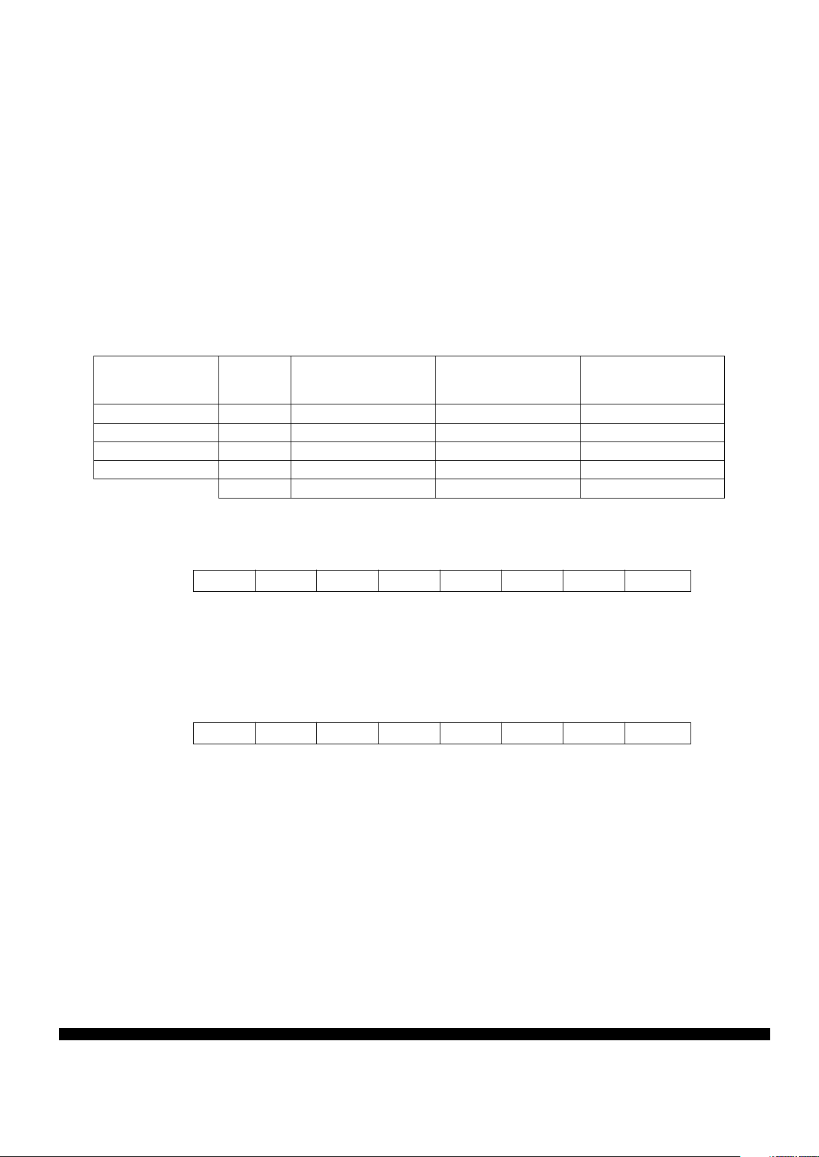
Table 4 MC68HC11KA4 Register and Control Bit Assignments
Bit 7 654321Bit 0
$0000 PA7 PA6 PA5 PA4 PA3 PA2 PA1 PA0 PORTA
$0001 DDA7 DDA6 DDA5 DDA4 DDA3 DDA2 DDA1 DDA0 DDRA
$0002 DDB7 DDB6 DDB5 DDB4 DDB3 DDB2 DDB1 DDB0 DDRB
$0003 DDF7 DDF6 DDF5 DDF4 DDF3 DDF2 DDF1 DDF0 DDRF
$0004 PB7 PB6 PB5 PB4 PB3 PB2 PB1 PB0 PORTB
$0005 PF7 PF6 PF5 PF4 PF3 PF2 PF1 PF0 PORTF
$0006 PC7 PC6 PC5 PC4 PC3 PC2 PC1 PC0 PORTC
$0007 DDC7 DDC6 DDC5 DDC4 DDC3 DDC2 DDC1 DDC0 DDRC
$0008 0 0 PD5 PD4 PD3 PD2 PD1 PD0 PORTD
$0009 0 0 DDD5 DDD4 DDD3 DDD2 DDD1 DDD0 DDRD
$000A PE7 PE6 PE5 PE4 PE3 PE2 PE1 PE0 PORTE
$000B FOC1 FOC2 FOC3 FOC4 FOC5 0 0 0 CFORC
$000C OC1M7 OC1M6 OC1M5 OC1M4 OC1M3 0 0 0 OC1M
$000D OC1D7 OC1D6 OC1D5 OC1D4 OC1D3 0 0 0 OC1D
$000E Bit 15 14 13 12 11 10 9 Bit 8 TCNT (High)
$000F Bit 7 654321Bit 0 TCNT (Low)
$0010 Bit 15 14 13 12 11 10 9 Bit 8 TIC1 (High)
$0011 Bit 7 654321Bit 0 TIC1 (Low)
$0012 Bit 15 14 13 12 11 10 9 Bit 8 TIC2 (High)
$0013 Bit 7 654321Bit 0 TIC2 (Low)
$0014 Bit 15 14 13 12 11 10 9 Bit 8 TIC3 (High)
$0015 Bit 7 654321Bit 0 TIC3 (Low)
$0016 Bit 15 14 13 12 11 10 9 Bit 8 TOC1(High)
$0017 Bit 7 654321Bit 0 TOC1 (Low)
$0018 Bit 15 14 13 12 11 10 9 Bit 8 TOC2 (High)
$0019 Bit 7 654321Bit 0 TOC2 (Low)
$001A Bit 15 14 13 12 11 10 9 Bit 8 TOC3 (High)
$001B Bit 7 654321Bit 0 TOC3 (Low)
$001C Bit 15 14 13 12 11 10 9 Bit 8 TOC4 (High)
$001D Bit 7 654321Bit 0 TOC4 (Low)
$001E Bit 15 14 13 12 11 10 9 Bit 8 TI4/O5 (High)
$001F Bit 7 654321Bit 0 TI4/O5 (Low)
$0020 OM2 OL2 OM3 OL3 OM4 OL4 OM5 OL5 TCTL1
$0021 EDG4B EDG4A EDG1B EDG1A EDG2B EDG2A EDG3B EDG3A TCTL2
$0022 OC1I OC2I OC3I OC4I I4/O5I IC1I IC2I IC3I TMSK1
$0023 OC1F OC2F OC3F OC4F I4/O5F IC1F IC2F IC3F TFLG1
$0024 TOI RTII PAOVI PAII 0 0 PR1 PR0 TMSK2
$0025 TOF RTIF PAOVF PAIF 0000TFLG2
$0026 0 PAEN PAMOD PEDGE 0 I4/O5 RTR1 RTR0 PACTL
$0027 Bit 7 654321Bit 0 PACNT
$0028 SPIE SPE DWOM MSTR CPOL CPHA SPR1 SPR0 SPCR
$0029 SPIF WCOL 0 MODF 0000SPSR
$002A Bit 7 654321Bit 0 SPDR
$002B MBE 0 ELAT EXCOL EXROW 0 0 EPGM EPROG

MOTOROLA MC68HC11KA4
16 MC68HC11KA4TS/D
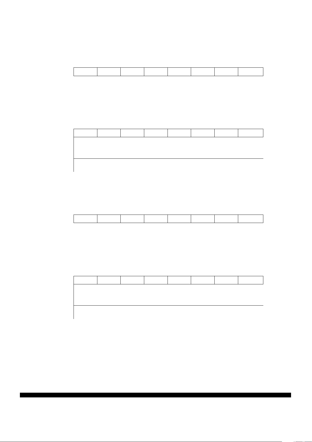
$002C 0000HPPUE GPPUE FPPUE BPPUE PPAR
$002D ————————Reserved
$002E ————————Reserved
$002F ————————Reserved
$0030 CCF 0 SCAN MULT CD CC CB CA ADCTL
$0031 Bit 7 654321Bit 0 ADR1
$0032 Bit 7 654321Bit 0 ADR2
$0033 Bit 7 654321Bit 0 ADR3
$0034 Bit 7 654321Bit 0 ADR4
$0035 BULKP LVPEN BPRT4 PTCON BPRT3 BPRT2 BPRT1 BPRT0 BPROT
$0036 ————————Reserved
$0037 EE3 EE2 EE1 EE0 0000INIT2
$0038 LIRDV CWOM 0 IRVNE LSBF SPR2 XDV1 XDV0 OPT2
$0039 ADPU CSEL IRQE DLY CME FCME CR1 CR0 OPTION
$003A Bit 7 654321Bit 0 COPRST
$003B ODD EVEN LVPI BYTE ROW ERASE EELAT EEPGM PPROG
$003C RBOOT SMOD MDA PSEL4 PSEL3 PSEL2 PSEL1 PSEL0 HPRIO
$003D RAM3 RAM2 RAM1 RAM0 REG3 REG2 REG1 REG0 INIT
$003E TILOP 0 OCCR CBYP DISR FCM FCOP 0 TEST1
$003F ROMAD 1 CLKX PAREN NOSEC NOCOP ROMON EEON CONFIG
$0040 ————————Reserved
to
$005F ————————Reserved
$0060 CON34 CON12 PCKA2 PCKA1 0 PCKB3 PCKB2 PCKB1 PWCLK
$0061 PCLK4 PCLK3 PCLK2 PCLK1 PPOL4 PPOL3 PPOL2 PPOL1 PWPOL
$0062 Bit 7 654321Bit 0 PWSCAL
$0063 TPWSL DISCP 0 0 PWEN4 PWEN3 PWEN2 PWEN1 PWEN
$0064 Bit 7 654321Bit 0 PWCNT1
$0065 Bit 7 654321Bit 0 PWCNT2
$0066 Bit 7 654321Bit 0 PWCNT3
$0067 Bit 7 654321Bit 0 PWCNT4
$0068 Bit 7 654321Bit 0 PWPER1
$0069 Bit 7 654321Bit 0 PWPER2
$006A Bit 7 654321Bit 0 PWPER3
$006B Bit 7 654321Bit 0 PWPER4
$006C Bit 7 654321Bit 0 PWDTY1
$006D Bit 7 654321Bit 0 PWDTY2
$006E Bit 7 654321Bit 0 PWDTY3
$006F Bit 7 654321Bit 0 PWDTY4
$0070 BTST BSPL 0 SBR12 SBR11 SBR10 SBR9 SBR8 SCBDH
$0071 SBR7 SBR6 SBR5 SBR4 SBR3 SBR2 SBR1 SBR0 SCBDL
$0072 LOOPS WOMS 0 M WAKE ILT PE PT SCCR1
$0073 TIE TCIE RIE ILIE TE RE RWU SBK SCCR2
$0074 TDRE TC RDRF IDLE OR NF FE PF SCSR1
$0075 0000000RAFSCSR2
Table 4 MC68HC11KA4 Register and Control Bit Assignments (Continued)
Bit 7 654321Bit 0

MC68HC11KA4 MOTOROLA
MC68HC11KA4TS/D 17
*The reset values of RBOOT, SMOD, and MDA depend on the mode selected at power up.
RBOOT — Read Bootstrap ROM
Valid only when SMOD is set to one (bootstrap or special test mode). Can only be written in special
mode.
0 = Bootloader ROM disabled and not in map
1 = Bootloader ROM enabled and in map at $BE00–$BFFF
SMOD and MDA —Special Mode Select and Mode Select A
These two bits can be read at any time. SMOD can only be written to zero. MDA can only be written
once in normal modes or any time in special modes.
PSEL[4:0] —Priority Select Bits [4:0]
Refer to 5 Resets and Interrupts.
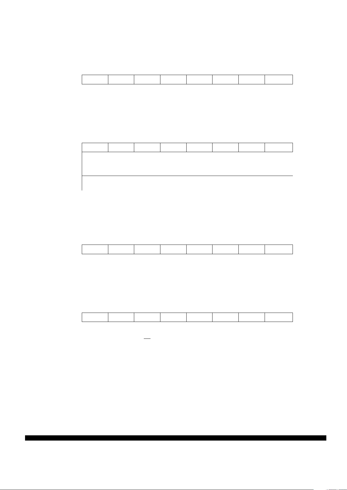
$0076 R8 T8 000000SCDRH
$0077 R7/T7 R6/T6 R5/T5 R4/T4 R3/T3 R2/T2 R1/T1 R0/T0 SCDRL
$0078 ————————Reserved
to
$007B ————————Reserved
$007C 0000PH3PH2PH1PH0PORTH
$007D 0000DDH3 DDH2 DDH1 DDH0 DDRH
$007E PG7 0000000PORTG
$007F DDG7 0000000DDRG
HPRIO — Highest Priority I-Bit Interrupt and Miscellaneous $003C
Bit 7 654321Bit 0
RBOOT* SMOD* MDA* PSEL4 PSEL3 PSEL2 PSEL1 PSEL0
RESET: 00000110Single Chip
00100110Expanded
11000110Bootstrap
01100110Special Test
Inputs Latched at Reset
MODB MODA Mode SMOD MDA
1 0 Single Chip 0 0
1 1 Expanded 0 1
0 0 Bootstrap 1 0
0 1 Special Test 1 1
Table 4 MC68HC11KA4 Register and Control Bit Assignments (Continued)
Bit 7 654321Bit 0

MOTOROLA MC68HC11KA4
18 MC68HC11KA4TS/D
Can be written only once in first 64 cycles out of reset in normal modes or at any time in special mode.
RAM[3:0] —Internal RAM Map Position
Specifies upper four bits of RAM address. At reset, RAM is mapped to $0000 along with register block.
REG[3:0] —128-Byte Register Block Map Position
Specifies upper four bits of register space address. At reset, registers are mapped to $0000.
CONFIG is made up of EEPROM cells and static working latches. The operation of the MCU is controlled directly by these latches and not the actual EEPROM byte. When programming the CONFIG register, the EEPROM byte is being accessed. When the CONFIG register is being read, the static latches
are being accessed.
These bits can be read at any time. The value read is the one latched into the register from the EEPROM cells during the last reset sequence. A new value programmed into this register cannot be read
until after a subsequent reset sequence. Unused bits always read as ones.
If SMOD = 1, CONFIG bits can be written at any time. If SMOD = 0 CONFIG bits can only be written
using the EEPROM programming sequence, and are neither readable nor active until latched via the
next reset.
ROMAD — ROM/EPROM Mapping Control
In single-chip mode ROMAD is forced to one out of reset.
0 = ROM/EPROM located at $2000–$7FFF ($2000–$9FFF in MC68HC11KA2)
1 = ROM/EPROM located at $A000–$FFFF ($8000–$FFFF in MC68HC11KA2)
Bit 6 — Not implemented
Always reads one
CLKX — XOUT Clock Enable
0 = XOUT pin disabled
1 = x clock driven out on the XOUT pin
PAREN — Pull-Up Assignment Register Enable
Refer to 6 Parallel Input/Output.
NOSEC — Security Disable
NOSEC is invalid unless the security mask option is specified before the MCU is manufactured. If security mask option is omitted NOSEC always reads one.
0 = Security enabled
1 = Security disabled
INIT —RAM and I/O Register Mapping $003D
Bit 7 654321Bit 0
RAM3 RAM2 RAM1 RAM0 REG3 REG2 REG1 REG0
RESET: 0000000 0
CONFIG —COP, ROM Mapping, EEPROM Enables $003F
Bit 7 654321Bit 0
ROMAD — CLKX PAREN NOSEC NOCOP ROMON EEON
RESET: — 1 — —————

MC68HC11KA4 MOTOROLA
MC68HC11KA4TS/D 19
NOCOP — COP System Disable
Resets to programmed value
0 = COP enabled (forces reset on time-out)
1 = COP disabled (does not force reset on time-out)
ROMON — ROM/EPROM Enable
In single-chip mode, ROMON is forced to one out of reset. In special test mode, ROMON is forced to
zero out of reset.
0 = ROM/EPROM removed from memory map
1 = ROM/EPROM present in memory map
EEON — EEPROM Enable
0 = EEPROM disabled from memory map
1 = EEPROM present in memory map with location depending on value specified in EE[3:0] in INIT2
Bit 7 — Not implemented
Always reads zero
CWOM — Port C Wired-OR Mode
Refer to 6 Parallel Input/Output.
Bit 5 — Not implemented
Always reads zero
IRVNE — Internal Read Visibility/Not E
Can be written at any time if SMOD = 1. If SMOD = 0, only one write is allowed. In expanded mode,
IRVNE determines whether IRV is on or off. In special test mode, IRVNE is reset to one. In all other
modes, IRVNE is reset to zero.
0 = No internal read visibility on external bus
1 = Data from internal reads is driven out of the external data bus.
In single-chip modes, this bit determines whether the E clock drives out from the chip.
0 = E is driven out from the chip.
1 = E pin is driven low.
LSBF — SPI LSB First Enable
Refer to 8 Serial Peripheral Interface.
SPR2 — SPI Clock Rate Select
Refer to 8 Serial Peripheral Interface.
OPT2 —System Configuration Options 2 $0038
Bit 7 654321Bit 0
— CWOM — IRVNE LSBF SPR2 XDV1 XDV0
RESET: 0 0 0 — 0 0 0 0
Mode IRVNE Out
of Reset
E Clock Out of
Reset
IRV Out of
Reset
IRVNE
Affects Only
IRVNE
Can Be Written
Single Chip 0 On Off E Once
Expanded 0 On Off IRV Once
Boot 0 On Off E Once
Special Test 1 On On IRV Once

MOTOROLA MC68HC11KA4
20 MC68HC11KA4TS/D
XDV[1:0] — XOUT Clock Divide Select
These two bits control the frequency of the clock that is driven out the XOUT pin. The CLKX bit in the
CONFIG register controls whether this clock is on or off. When a clock rate is selected, allow a maximum of 16 cycles for stabilization. During reset a frequency of EXTAL is output. This frequency can be
divided after reset. Note that the phase relationship between the 4XDV1 signal and both EXTAL and E
cannot be predicted. Refer to the following table for further information about XOUT frequencies.
NOTE
The XOUT pin is not bonded in the 64-pin package.
Table 5 XOUT Frequencies
XDV[1:0] EXTAL
Divided By
Frequency at
EXTAL = 8 MHz
Frequency at
EXTAL = 12 MHz
Frequency at
EXTAL = 16 MHz
0 0 1 8 MHz 12 MHz 16 MHz
0 1 4 2 MHz 3 MHz 4 MHz
1 0 6 1.33 MHz 2 MHz 2.7 MHz
1 1 8 1 MHz 1.5 MHz 2 MHz
XDV[1:0] EXTAL
Divided By
Frequency at
EXTAL = 8.4 MHz
Frequency at
EXTAL = 12.6 MHz
Frequency at
EXTAL = 16.8 MHz
0 0 1 8.4 MHz 12.6 MHz 16.8 MHz
0 1 4 2.1 MHz 3.15 MHz 4.2 MHz
1 0 6 1.4 MHz 2.1 MHz 2.8 MHz
1 1 8 1.05 MHz 1.57 MHz 2.1 MHz

MC68HC11KA4 MOTOROLA
MC68HC11KA4TS/D 21
3 Erasable Programmable Read-Only Memory
The MC68HC711KA4 has 24 Kbytes of ROM/EPROM. The MC68HC711KA2 has 32 Kbytes of ROM/
EPROM. In all parts, the ROM/EPROM can be mapped to one of two locations in the memory map. The
locations are as follows:
In the MC68HC11KA4, the ROM/EPROM can be mapped at $2000–$7FFF or $A000–$FFFF. If it is
mapped to $A000–$FFFF, vector space is included. In single-chip mode the MC68HC11KA4 ROM/
EPROM is forced to $A000–$FFFF (ROMAD = 1) and enabled (ROMON = 1), regardless of the value
in the CONFIG register.
In the MC68HC11KA2, the ROM/EPROM can be mapped at $0000–$7FFF or $8000–$FFFF. If it is
mapped to $8000–$FFFF, vector space is included. In single-chip mode the MC68HC11KA2 ROM/
EPROM is forced to $8000–$FFFF (ROMAD = 1) and enabled (ROMON = 1), regardless of the value
in the CONFIG register.
In PROG mode, the EPROM/OTPROM is programmed as a stand-alone EPROM by adapting the MCU
footprint to the 27256-type EPROM and using an appropriate EPROM programmer. Programming
EPROM/OTPROM requires an external 12.25 volt nominal power supply (V
PPE
). There are two meth-
ods that can be used to program and verify EPROM/OTPROM.
In normal MCU mode, EPROM/OTPROM can be programmed in any operating mode —special test,
bootstrap, expanded, or single chip. Normal programming is completed using the EPROG register.
To program the EPROM, complete the following steps using the EPROG register:
1. Write to EPROG with the ELAT bit set.
2. Write data to the desired address.
3. Write to EPROG with the ELAT and EPGM bits set.
4. Delay for 10 ms or more, as appropriate.
5. Clear the EPGM bit in EPROG to turn off the V
PPE
voltage.
6. Clear the EPROG register to reconfigure the EPROM address and data buses for normal operation.
MBE — Multiple Byte Program Enable
Used for factory test purposes only
Bit 6 — Not implemented
Always reads zero
ELAT — EPROM Latch Control
If ELAT = 1, EPROM is in programming mode and cannot be read. If ELAT = 1, writes to EPROM cause
address and data to be latched.
0 = EPROM address and data bus configured for normal reads
1 = EPROM address and data bus configured for programming
EXCOL — Select Extra Columns
Used for factory test purposes only
EXROW — Select Extra Row
Used for factory test purposes only
Bits [2:1] — Not implemented
Always read zero
EPROG —EPROM Programming Control $002B
Bit 7 654321Bit 0
MBE — ELAT EXCOL EXROW — — EPGM
RESET: 0000000 0

MOTOROLA MC68HC11KA4
22 MC68HC11KA4TS/D
EPGM — EPROM Program Command
If ELAT = 1 then EPGM = 0.
0 = Programming power to EPROM array switched off
1 = Power to EPROM array switched on
Figure 8 Wiring Diagram for MC68HC711KA4/KA2 EPROM in PROG Mode
NOTES:
PF4/ADDR4
PF5/ADDR5
PF6/ADDR6
PF1/ADDR1
PF2/ADDR2
PF3/ADDR3
PF7/ADDR7
PF0/ADDR0
ADDR4
ADDR5
ADDR6
ADDR1
ADDR2
ADDR3
ADDR7
ADDR12
ADDR8
ADDR9
ADDR10
ADDR11
ADDR0
PB6/ADDR14
PB4/ADDR12
PB0/ADDR8
PB1/ADDR9
PB2/ADDR10
PB3/ADDR11
PC7/DATA7
PC6/DATA6
PC5/DATA5
PC4/DATA4
PC3/DATA3
PC2/DATA2
PC1/DATA1
PC0/DATA0
O7
O6
O5
O1
O2
O4
O3
O0
ADDR4
ADDR5
ADDR6
ADDR1
ADDR2
ADDR3
ADDR7
ADDR12
ADDR8
ADDR9
ADDR10
ADDR11
ADDR0
ADDR14
O7
O6
O5
O1
O2
O4
O3
O0
INTERNAL
24 KBYTE
(32 KBYTES, KA2)
EPROM
PIN FUNCTIONS
MCU PIN FUNCTIONS
EPROM MODE PIN CONNECTIONS
MC68HC711KA4
IRQ
XIRQ/V
PPE
PB7/ADDR15
CE
OE
PB5/ADDR13
ADDR13
ADDR13
GND
GND PA0/IC3
PA3/IC4/OC5/OC1
V
SS
CE
OE
V
CC
V
PP
PE0/AN0
ADDR14
GND PA1/IC2
GND PA2/IC1
GND PA4/OC4/OC1
GND PA5/OC3/OC1
GND PA6/OC2/OC1
GND PA7/PAI/OC1
GND PG7/R/W
GND PD0/RxD
GND PD1/TxD
PD2/MISO
PD3/MOSI
PD4/SCK
PD5/SS
UNUSED
GND
GND
GND
GND
V
RL
V
RH
EXTAL
XTAL
E
MODA/LIR
MODB/V
STBY
RESET
GND
GND
GND
UNUSED
GNDPH0/PW1
PH1/PW2
PH2/PW3
PH3/PW4
TESTxx (3)
XOUT
PE1/AN1
PE2/AN2
PE3/AN3
PE4/AN4
PE5/AN5
PE6/AN6
PE7/AN7
GND
GND
GND
GND
GND
GND
V
SS
V
SS
V
DD
V
CC
V
PP
OUTPUTS
INPUTS
NOTE 3
NOTE 4
NOTE 1
NOTE 2
NOTE 1
NOTE 4
1. Unused Inputs – grounding is recommended.
2. Unused Inputs – these pins may be left unterminated.
3. Unused Outputs – these pins should be left unconnected.
4. Grounding these six pins configures the MC68HC711KA4/KA2 for EPROM emulation mode.
EPROM
27256
FOOTPRINT
MC68HC711KA2

MC68HC11KA4 MOTOROLA
MC68HC11KA4TS/D 23
4 Electrically Erasable Programmable Read-Only Memory
The 640-byte on-chip EEPROM is initially located from $0D80 to $0FFF after reset in all modes. It can
be mapped to any other 4 Kbyte boundary by writing to the INIT2 register. The EEPROM is enabled by
the EEON bit in the CONFIG register. Programming and erasing is controlled by the PPROG register.
An internal oscillator clock-run charge pump supplies the programming voltage. Use of the block protect
register (BPROT) prevents inadvertent writes to (or erases of) blocks of EEPROM. The CSEL bit in the
OPTION register selects the on-chip oscillator clock for programming and erasing while operating at frequencies below 1 MHz. Refer to 5 Resets and Interrupts.
In special mode there is an extra row of 16 bytes of EEPROM (located at $0D60), which is used for
factory testing. Endurance and data retention specifications do not apply to this row.
The erased state of EEPROM is $FF (all ones).
To erase the EEPROM, ensure that the proper bits of the BPROT register are cleared, then complete
the following steps using the PPROG register:
1. Write to PPROG with the ERASE, EELAT, and appropriate BYTE and ROW bits set.
2. Write to the appropriate EEPROM address with any data. Row erase only requires a write to
any location in the row. Bulk erase is accomplished by writing to any location in the array.
3. Write to PPROG with ERASE, EELAT, EEPGM, and the appropriate BYTE and ROW bits set.
4. Delay for 10 ms or more, as appropriate.
5. Clear the EEPGM bit in PPROG to turn off the high voltage.
6. Clear the PPROG register to reconfigure the EEPROM address and data buses for normal operation.
To program the EEPROM, ensure the proper bits of the BPROT register are cleared, then complete the
following steps using the PPROG register:
1. Write to PPROG with the EELAT bit set.
2. Write data to the desired address.
3. Write to PPROG with the EELAT and EEPGM bits set.
4. Delay for 10 ms or more, as appropriate.
5. Clear the EEPGM bit in PPROG to turn off the high voltage.
6. Clear the PPROG register to reconfigure the EEPROM address and data buses for normal operation.
CAUTION
Since it is possible to perform other operations while the EEPROM programming/
erase operation is in progress, it is fairly common to start the operation then return
to the main program until the 10 ms is completed. When the EELAT bit is set at the
beginning of a program/erase operation, the EEPROM is electronically removed
from the memory map; thus, it is not accessible during the program/erase cycle.
Care must be taken to ensure that EEPROM resources will not be needed by any
routines in the code during the 10 ms program/erase time.

MOTOROLA MC68HC11KA4
24 MC68HC11KA4TS/D
NOTE
Block protect register bits can be written to zero (protection disabled) only once
within 64 cycles of a reset in normal modes, or at any time in special mode. Block
protect register bits can be written to one (protection enabled) at any time.
BULKP — Bulk Erase of EEPROM Protect
0 = EEPROM can be bulk erased normally
1 = EEPROM cannot be bulk or row erased
LVPEN — Low Voltage Programming Protect Enable
If LVPEN = 1, programming of the EEPROM is enabled unless the LVPI circuit detects that VDD has
fallen below a safe operating voltage thus setting the low voltage programming inhibit bit in PPROG reg-
ister (LVPI = 1).
0 = Low voltage programming protect for EEPROM disabled
1 = Low voltage programming protect for EEPROM enabled
BPRT[4:0] —Block Protect Bits for EEPROM
0 = Protection disabled
1 = Protection enabled
PTCON — Protect for CONFIG
0 = CONFIG register can be programmed or erased normally
1 = CONFIG register cannot be programmed or erased
INIT2 can be written only once in normal modes, any time in special modes.
EE[3:0] — EEPROM Map Position
EEPROM is at $xD80–$xFFF, where x is the hexadecimal digit represented by EE[3:0] bits.
Bits [3:0] — Not implemented
Always read zero
BPROT —Block Protect $0035
Bit 7 654321Bit 0
BULKP LVPEN BPRT4 PTCON BPRT3 BPRT2 BPRT1 BPRT0
RESET: 1111111 1
Bit Name Block Protected Block Size
BPRT4 $xF80–$xFFF 128 Bytes
BPRT3 $xE60–$xF7F 288 Bytes
BPRT2 $xDE0–$xE5F 128 Bytes
BPRT1 $xDA0–$xDDF 64 Bytes
BPRT0 $xD80–$xD9F 32 Bytes
INIT2 —EEPROM Mapping $0037
Bit 7 654321Bit 0
EE3 EE2 EE1 EE0 — — — —
RESET: 0000000 0

MC68HC11KA4 MOTOROLA
MC68HC11KA4TS/D 25
ODD — Program Odd Rows in Half of EEPROM (TEST)
EVEN — Program Even Rows in Half of EEPROM (TEST)
LVPI — Low Voltage Programming Inhibit
LVPI can be read at any time and writes to LVPI have no meaning nor effect. LVPI is set if LVPEN bit
in BPROT register equals 1 and the LVPI circuit detects that VDD has fallen below a safe operating volt-
age. Once set, LVPI is cleared when V
DD
returns to a safe operating voltage or if LVPEN bit in BPROT
register is cleared. If LVPEN = 0, then LVPI is always zero and has no meaning nor effect.
0 = EEPROM programming enabled
1 = EEPROM programming disabled
BYTE — Byte/Other EEPROM Erase Mode
0 = Row or bulk erase mode used
1 = Erase only one byte of EEPROM
ROW — Row/All EEPROM Erase Mode (only valid when BYTE = 0)
0 = All 640 bytes of EEPROM erased
1 = Erase only one 16-byte row of EEPROM
ERASE — Erase/Normal Control for EEPROM
0 = Normal read or program mode
1 = Erase mode
EELAT — EEPROM Latch Control
0 = EEPROM address and data bus configured for normal reads
1 = EEPROM address and data bus configured for programming or erasing
EEPGM — EEPROM Program Command
0 = Program or erase voltage switched off to EEPROM array
1 = Program or erase voltage switched on to EEPROM array
Refer also to INIT2 register.
PPROG — EEPROM Programming Control $003B
Bit 7 654321Bit 0
ODD EVEN LVPI BYTE ROW ERASE EELAT EEPGM
RESET: 0000000 0
BYTE ROW Action
0 0 Bulk Erase (All 640 Bytes)
0 1 Row Erase (16 Bytes)
1 0 Byte Erase
1 1 Byte Erase

MOTOROLA MC68HC11KA4
26 MC68HC11KA4TS/D
5 Resets and Interrupts
The MC68HC11KA4/KA2 has three reset vectors and 18 interrupt vectors. The reset vectors are as follows:
• RESET, or Power-On Reset
• Clock Monitor Fail
• COP Failure
The 18 interrupt vectors service 22 interrupt sources (three non-maskable, 19 maskable). The three
nonmaskable interrupt vectors are as follows:
• XIRQ Pin (X-Bit Interrupt)
• Illegal Opcode Trap
• Software Interrupt
On-chip peripheral systems generate maskable interrupts, which are recognized only if the global interrupt mask bit (I) in the condition code register (CCR) is clear. Maskable interrupts are prioritized according to a default arrangement; however, any one source can be elevated to the highest maskable priority
position by a software-accessible control register (HPRIO). The HPRIO register can be written at any
time, provided bit I in the CCR is set.
Nineteen interrupt sources in the MC68HC11KA4/KA2 are subject to masking by the global interrupt
mask bit (bit I in the CCR). In addition to the global bit I, all of these sources, except the external interrupt
(IRQ
) pin, are controlled by local enable bits in control registers. Most interrupt sources in the M68HC11
have separate interrupt vectors; therefore, there is usually no need for software to poll control registers
to determine the cause of an interrupt.
For some interrupt sources, such as the SCI interrupts, the flags are automatically cleared during the
normal course of responding to the interrupt requests. For example, the RDRF flag in the SCI system
is cleared by the automatic clearing mechanism consisting of a read of the SCI status register while
RDRF is set, followed by a read of the SCI data register. The normal response to an RDRF interrupt
request would be to read the SCI status register to check for receive errors, then to read the received
data from the SCI data register. These two steps satisfy the automatic clearing mechanism without requiring any special instructions.
Refer to the following table for a list of interrupt and reset vector assignments

MC68HC11KA4 MOTOROLA
MC68HC11KA4TS/D 27
*Can be written only once in first 64 cycles out of reset in normal mode, or at any time in special mode.
ADPU —A/D Converter Power-Up
Refer to 9 Analog-to-Digital Converter.
CSEL —Clock Select
Refer to 9 Analog-to-Digital Converter.
IRQE —IRQ Select Edge Sensitive Only
0 = Low level recognition
1 = Falling edge recognition
Vector Address Interrupt Source CCR
Mask Bit
Local Mask
FFC0, C1 – FFD4, D5 Reserved — —
FFD6, D7 SCI Serial System I
• SCI Receive Data Register Full RIE
• SCI Receiver Overrun RIE
• SCI Transmit Data Register Empty TIE
• SCI Transmit Complete TCIE
• SCI Idle Line Detect ILIE
FFD8, D9 SPI Serial Transfer Complete I SPIE
FFDA, DB Pulse Accumulator Input Edge I PAII
FFDC, DD Pulse Accumulator Overflow I PAOVI
FFDE, DF Timer Overflow I TOI
FFE0, E1 Timer Input Capture 4/Output Compare 5 I I4/O5I
FFE2, E3 Timer Output Compare 4 I OC4I
FFE4, E5 Timer Output Compare 3 I OC3I
FFE6, E7 Timer Output Compare 2 I OC2I
FFE8, E9 Timer Output Compare 1 I OC1I
FFEA, EB Timer Input Capture 3 I IC3I
FFEC, ED Timer Input Capture 2 I IC2I
FFEE, EF Timer Input Capture 1 I IC1I
FFF0, F1 Real-Time Interrupt I RTII
FFF2, F3 IRQ
I None
FFF4, F5 XIRQ
Pin X None
FFF6, F7 Software Interrupt None None
FFF8, F9 Illegal Opcode Trap None None
FFFA, FB COP Failure None NOCOP
FFFC, FD Clock Monitor Fail None CME
FFFE, FF RESET None None
OPTION —System Configuration Options $0039
Bit 7 654321Bit 0
ADPU CSEL IRQE* DLY CME FCME* CR1* CR0*
RESET: 0001000 0
MOTOROLA MC68HC11KA4
28 MC68HC11KA4TS/D
DLY —Enable Oscillator Start-Up Delay on Exit from STOP
0 = No stabilization delay on exit from STOP
1 = Stabilization delay enabled on exit from STOP
CME — Clock Monitor Enable
0 = Clock monitor disabled; slow clocks can be used
1 = Slow or stopped clocks cause clock failure reset
FCME — Force Clock Monitor Enable
0 = Clock monitor follows the state of the CME bit
1 = Clock monitor circuit is enabled until next reset
CR[1:0] — COP Timer Rate Select
Write $55 to COPRST to arm COP watchdog clearing mechanism. Write $AA to COPRST to reset COP
watchdog.
*RBOOT, SMOD, and MDA reset depend on power-up initialization mode and can only be written in special mode.
RBOOT — Read Bootstrap ROM
Refer to 2 Operating Modes and On-Chip Memory.
SMOD — Special Mode Select
Refer to 2 Operating Modes and On-Chip Memory.
MDA — Mode Select A
Refer to 2 Operating Modes and On-Chip Memory.
Table 6 COP Timer Rate Select
CR[1:0] Divide
E/2
15
By
XTAL = 8.0 MHz
Time-out
–0/+16.4 ms
XTAL = 12.0 MHz
Time-out
–0/+10.9 ms
XTAL = 16.0 MHz
Time-out
–0/+8.2 ms
0 0 0 1 16.384 ms 10.923 ms 8.192 ms
0 0 1 4 65.536 ms 43.691 ms 32.768 ms
0 1 0 16 262.14 ms 174.76 ms 131.07 ms
0 1 1 64 1.049 s 699.05 ms 524.29 ms
E = 2.0 MHz 3.0 MHz 4.0 MHz
COPRST — Arm/Reset COP Timer Circuitry $003A
Bit 7 654321Bit 0
76543210
RESET: 0000000 0
HPRIO — Highest Priority I-Bit Interrupt and Miscellaneous $003C
Bit 7 654321Bit 0
RBOOT* SMOD* MDA* PSEL4 PSEL3 PSEL2 PSEL1 PSEL0
RESET: — — — 0011 0

MC68HC11KA4 MOTOROLA
MC68HC11KA4TS/D 29
PSEL[4:0] — Priority Select Bits [4:0]
Can be written only while bit I in the CCR is set (interrupts disabled). These bits select one interrupt
source to be elevated above all other I-bit related sources.
CONFIG is made up of EEPROM cells and static latches. The operation of the MCU is controlled directly
by these latches and not the actual EEPROM byte. When programming the CONFIG register, the EEPROM byte is being accessed. When the CONFIG register is being read, the static latches are being
accessed.
These bits can be read at any time. The value read is the one latched into the register from the EEPROM cells during the last reset sequence. A new value programmed into this register cannot be read
until after a subsequent reset sequence. Unused bits always read as ones.
If SMOD = 1, CONFIG bits can be written at any time. If SMOD = 0 CONFIG bits can only be written
using the EEPROM programming sequence, and are neither readable nor active until latched via the
next reset.
ROMAD — ROM/EPROM Mapping Control
Refer to 2 Operating Modes and On-Chip Memory.
PSELx
Interrupt Source Promoted
43210
0 0 0 X X Reserved (Default to IRQ
)
00100Reserved (Default to IRQ
)
00101Reserved (Default to IRQ
)
00110IRQ
00111Real-Time Interrupt
01000Timer Input Capture 1
01001Timer Input Capture 2
01010Timer Input Capture 3
01011Timer Output Compare 1
01100Timer Output Compare 2
01101Timer Output Compare 3
01110Timer Output Compare 4
01111Timer Input Capture 4/Output Compare 5
10000Timer Overflow
10001Pulse Accumulator Overflow
10010Pulse Accumulator Input Edge
10011SPI Serial Transfer Complete
10100SCI Serial System
10101Reserved (Default to IRQ
)
10110Reserved (Default to IRQ
)
10111Reserved (Default to IRQ
)
1 1 X X X Reserved (Default to IRQ
)
CONFIG — COP, ROM Mapping, EEPROM Enables $003F
Bit 7 654321Bit 0
ROMAD — CLKX PAREN NOSEC NOCOP ROMON EEON
RESET: — 1 — ———— —

MOTOROLA MC68HC11KA4
30 MC68HC11KA4TS/D
Bit 6 — Not implemented
Always reads one
CLKX — XOUT Clock
Refer to 2 Operating Modes and On-Chip Memory.
PAREN — Pull-Up Assignment Register Enable
Refer to 6 Parallel Input/Output.
NOSEC — Security Disable
Refer to 2 Operating Modes and On-Chip Memory.
NOCOP — COP System Disable
Resets to programmed value
0 = COP enabled (forces reset on time-out)
1 = COP disabled (does not force reset on time-out)
ROMON — ROM/EPROM Enable
Refer to 2 Operating Modes and On-Chip Memory.
EEON — EEPROM Enable
Refer to 2 Operating Modes and On-Chip Memory.

MC68HC11KA4 MOTOROLA
MC68HC11KA4TS/D 31
6 Parallel Input/Output
The MC68HC11KA4/KA2 has up to 51 input/output lines, depending on the operating mode. To enhance the I/O functions, the data bus of this microcontroller is non-multiplexed. The following table is a
summary of the configuration and features of each port.
* Only four pins on 64-pin version.
ROMAD — ROM Mapping Control
Refer to 2 Operating Modes and On-Chip Memory.
Bit 6 — Not implemented
Always reads one
CLKX — XOUT Clock Enable
Refer to 2 Operating Modes and On-Chip Memory.
PAREN — Pull-Up Assignment Register Enable
0 = Pull-ups always disabled regardless of state of bits in PPAR
1 = Pull-ups either enabled or disabled through PPAR
NOSEC — Security Disable
Refer to 2 Operating Modes and On-Chip Memory.
NOCOP — COP System Disable
Refer to 5 Resets and Interrupts.
ROMON — ROM/EPROM Enable
Refer to 2 Operating Modes and On-Chip Memory.
EEON — EEPROM Enable
Refer to 2 Operating Modes and On-Chip Memory.
Port Input Pins Output Pins Bidirectional Pins Shared Functions
Port A — — 8 Timer
Port B — — 8 High Order Address
Port C — — 8 Data Bus
Port D — — 6 SCI and SPI
Port E 8* — — A/D Converter
Port F — — 8 Low Order Address
Port G — — 1 R/W
Signal
Port H — — 4 PWMs
CONFIG — COP, ROM Mapping, EEPROM Enables $003F
Bit 7 654321Bit 0
ROMAD — CLKX PAREN NOSEC NOCOP ROMON EEON
RESET: — 1 ————— —

MOTOROLA MC68HC11KA4
32 MC68HC11KA4TS/D
LIRDV — LIR Driven
Refer to 2 Operating Modes and On-Chip Memory.
CWOM — Port C Wired-OR Mode
0 = Port C operates normally.
1 = Port C outputs are open-drain.
Bit 5 — Not implemented
Always reads zero
IRVNE — Internal Read Visibility/Not E
Refer to 2 Operating Modes and On-Chip Memory.
LSBF — SPI LSB First Enable
Refer to 8 Serial Peripheral Interface.
SPR2 — SPI Clock (SCK) Rate Select
Refer to 8 Serial Peripheral Interface.
XDV1, XDV0 — XOUT Clock Divide Select
Refer to 2 Operating Modes and On-Chip Memory.
NOTE
Do not confuse pin function with the electrical state of the pin at reset. All generalpurpose I/O pins configured as inputs at reset are in a high-impedance state and
the contents of port data registers is undefined. In port descriptions, a “U” indicates
this condition. The pin function is mode dependent.
NOTE
To enable PA3 as fourth input capture, set the I4/O5 bit in the PACTL register. Otherwise, PA3 is configured as a fifth output compare out of reset, with bit I4/O5 being
cleared. If the DDA3 bit is set (configuring PA3 as an output), and IC4 is enabled,
writes to PA3 cause edges on the pin to result in input captures. Writing to TI4/O5
has no effect when the TI4/O5 register is acting as IC4. PA7 drives the pulse accumulator input but also can be configured for general-purpose I/O, or output compare. Note that even when PA7 is configured as an output, the pin still drives the
pulse accumulator input.
OPT2 —System Configuration Options 2 $0038
Bit 7 654321Bit 0
LIRDV CWOM — IRVNE LSBF SPR2 XDV1 XDV0
RESET: 0 0 0 — 0 0 0 0
PORTA —Port A Data $0000
Bit 7 654321Bit 0
PA7 PA6 PA5 PA4 PA3 PA2 PA1 PA0
RESET: UUUUUUU U
Alt. Pin
Func.: PAI OC2 OC3 OC4 IC4/OC5 IC1 IC2 IC3
And/or: OC1 OC1 OC1 OC1 OC1 — — —
MC68HC11KA4 MOTOROLA
MC68HC11KA4TS/D 33
DDA[7:0] —Data Direction for Port A
0 = Bits set to zero to configure corresponding I/O pin for input only
1 = Bits set to one to configure corresponding I/O pin for output
Reset state is mode dependent. In single-chip or bootstrap modes, port B pins are high impedance inputs with selectable internal pull-up resistors. In expanded or test modes, port B pins are high order address outputs and PORTB is not in the memory map.
DDB[7:0] — Data Direction for Port B
0 = Bits set to zero to configure corresponding I/O pin for input only
1 = Bits set to one to configure corresponding I/O pin for output
Reset state is mode dependent. In single-chip or bootstrap modes, port F pins are high-impedance inputs with selectable internal pull-up resistors. In expanded or test modes, port F pins are low order address outputs and PORTF is not in the memory map.
DDRA — Data Direction Register for Port A $0001
Bit 7 654321Bit 0
DDA7 DDA6 DDA5 DDA4 DDA3 DDA2 DDA1 DDA0
RESET: 0000000 0
PORTB —Port B Data $0004
Bit 7 654321Bit 0
PB7 PB6 PB5 PB4 PB3 PB2 PB1 PB0
S. Chip or
Boot: PB7 PB6 PB5 PB4 PB3 PB2 PB1 PB0
RESET: UUUUUUU U
Expan. or
Test: ADDR15 ADDR14 ADDR13 ADDR12 ADDR11 ADDR10 ADDR9 ADDR8
DDRB — Data Direction Register for Port B $0002
Bit 7 654321Bit 0
DDB7 DDB6 DDB5 DDB4 DDB3 DDB2 DDB1 DDB0
RESET: 0000000 0
PORTF — Port F Data $0005
Bit 7 654321Bit 0
PF7 PF6 PF5 PF4 PF3 PF2 PF1 PF0
S. Chip or
Boot: PF7 PF6 PF5 PF4 PF3 PF2 PF1 PF0
RESET: UUUUUUU U
Expan. or
Test: ADDR7 ADDR6 ADDR5 ADDR4 ADDR3 ADDR2 ADDR1 ADDR0
MOTOROLA MC68HC11KA4
34 MC68HC11KA4TS/D
DDF[7:0] — Data Direction for Port F
0 = Bits set to zero to configure corresponding I/O pin for input only
1 = Bits set to one to configure corresponding I/O pin for output
Reset state is mode dependent. In single-chip or bootstrap modes, port C pins are high-impedance inputs. It is customary to have an external pull-up resistor on lines that are driven by open-drain devices.
In expanded or test modes, port C pins are data bus inputs and outputs and PORTC is not in the memory map.
DDC[7:0] — Data Direction for Port C
0 = Bits set to zero to configure corresponding I/O pin for input only
1 = Bits set to one to configure corresponding I/O pin for output
DDRF —Data Direction Register for Port F $0003
Bit 7 654321Bit 0
DDF7 DDF6 DDF5 DDF4 DDF3 DDF2 DDF1 DDF0
RESET: 0000000 0
PORTC —Port C Data $0006
Bit 7 654321Bit 0
PC7 PC6 PC5 PC4 PC3 PC2 PC1 PC0
S. Chip or
Boot: PC7 PC6 PC5 PC4 PC3 PC2 PC1 PC0
RESET: 0000000 0
Expan. or
Test: DATA7 DATA6 DATA5 DATA4 DATA3 DATA2 DATA1 DATA0
DDRC — Data Direction Register for Port C $0007
Bit 7 654321Bit 0
DDC7 DDC6 DDC5 DDC4 DDC3 DDC2 DDC1 DDC0
RESET: 0000000 0
PORTD — Port D Data $0008
Bit 7 654321Bit 0
0 0 PD5 PD4 PD3 PD2 PD1 PD0
RESET: 0 0 UUUUUU
Alt. Pin
Func.: — — SS
SCK MOSI MISO TxD RxD

MC68HC11KA4 MOTOROLA
MC68HC11KA4TS/D 35
Bits [7:6] —Not implemented
Always read zero
DDD[5:0] — Data Direction for Port D
0 = Bits set to zero to configure corresponding I/O pin for input only
1 = Bits set to one to configure corresponding I/O pin for output
NOTE
When the SPI system is in slave mode, DDD5 has no meaning nor effect. When
the SPI system is in master mode, DDD5 determines whether bit 5 of PORTD is an
error detect input (DDD5 = 0) or a general-purpose output (DDD5 = 1). If the SPI
system is enabled and expects any of bits [4:2] to be an input that bit will be an input
regardless of the state of the associated DDR bit. If any of bits [4:2] are expected
to be outputs that bit will be an output only if the associated DDR bit is set.
*Not bonded on 64-pin version.
Bits [7:4] — Not implemented
Always read zero
xPPUE — Port x Pin Pull-Up Enable
Refer to PAREN bit in CONFIG register discussed in 6 Parallel Input/Output.
0 = Port x pin on-chip pull-up devices disabled
1 = Port x pin on-chip pull-up devices enabled
NOTE
FPPUE and BPPUE do not apply in expanded mode because ports F and B are
address outputs.
DDRD — Data Direction Register for Port D $0009
Bit 7 654321Bit 0
— — DDD5 DDD4 DDD3 DDD2 DDD1 DDD0
RESET: 0000000 0
PORTE — Port E Data $000A
Bit 7 654321Bit 0
PE7* PE6* PE5* PE4* PE3 PE2 PE1 PE0
RESET: UUUUUUU U
Alt. Pin
Func.: AN7 AN6 AN5 AN4 AN3 AN2 AN1 AN0
PPAR —Port Pull-Up Assignment $002C
Bit 7 654321Bit 0
————HPPUE GPPUE FPPUE BPPUE
RESET: 0000111 1

MOTOROLA MC68HC11KA4
36 MC68HC11KA4TS/D
Port H pins reset to high-impedance inputs with selectable internal pull-up resistors.
Bits [7:4] — Not implemented
Always read zero
DDH[3:0] — Data Direction for Port H
0 = Bits set to zero to configure corresponding I/O pin for input only
1 = Bits set to one to configure corresponding I/O pin for output
NOTE
In any mode, PWM circuitry forces the I/O state to be an output for each port H line
associated with an enabled pulse-width modulator channel. In these cases, data
direction bits are not changed and have no effect on these lines. DDRH reverts to
controlling the I/O state of a pin when the associated function is disabled. Refer to
12 Pulse-Width Modulation Timer for further information.
Port G pins reset to high-impedance inputs with selectable internal pull-up resistors. In expanded and
special test modes PG7 becomes R/W
.
DDG7 — Data Direction for Port G
0 = Bit set to zero to configure corresponding I/O pin for input only
1 = Bit set to one to configure corresponding I/O pin for output
In expanded and test modes, bit 7 is configured for R/W, forcing the state of this pin to be an output
although the DDRG value remains zero.
Bits [6:0] — Not implemented
Always read zero
PORTH — Port H Data $007C
Bit 7 654321Bit 0
————PH3PH2PH1PH0
RESET: 0000UUUU
Alt. Pin
Func.:
————PW4PW3PW2PW1
DDRH — Data Direction Register for Port H $007D
Bit 7 654321Bit 0
————DDH3 DDH2 DDH1 DDH0
RESET: 0000111 1
PORTG — Port G Data $007E
Bit 7 654321Bit 0
PG7—————— —
RESET: U 000000 0
Alt. Pin
Func.: R/W
———————
DDRG — Data Direction Register for Port G $007F
Bit 7 654321Bit 0
DDG7 ———————
RESET: 0000000 0

MC68HC11KA4 MOTOROLA
MC68HC11KA4TS/D 37
7 Serial Communications Interface
The SCI, a universal asynchronous receiver transmitter (UART) serial communications interface, is one
of two independent serial I/O subsystems in the MC68HC11KA4/KA2. Rearranging registers and control bits used in previous M68HC11 family devices has enhanced the existing SCI system and added
new features, which include the following:
• A 13-bit modulus prescaler that allows greater baud rate control
• A new idle mode detect, independent of preceding serial data
• A receiver active flag
• Hardware parity for both transmitter and receiver
The enhanced baud rate generator is shown in the following diagram. Refer to the table of SCI baud
rate control values for standard values.
Figure 9 SCI Baud Generator Circuit Diagram
SCI BAUD GENERATOR
÷3 ÷4 ÷13
OSCILLATOR
AND
CLOCK GENERATOR
(÷4)
XTAL
EXTAL
E
AS
INTERNAL BUS CLOCK (PH2)
1:1
SCP[1:0]
1:00:10:0
÷2
0:0:0
÷2
0:0:1
÷2
0:1:0
÷2
0:1:1
÷2
1:0:0
÷2
1:0:1
÷2
1:1:0
1:1:1
÷16
SCI
RECEIVE
BAUD RATE
(16X)
SCR[2:0]
SCI
TRANSMIT
BAUD RATE
(1X)

MOTOROLA MC68HC11KA4
38 MC68HC11KA4TS/D
Figure 10 SCI Transmitter Block Diagram
FE
NF
OR
IDLE
RDRF
TC
TDRE
SCSR INTERRUPT STATUS
SBK
RWU
RE
TE
ILIE
RIE
TCIE
TIE
SCCR2 SCI CONTROL 2
TRANSMITTER
CONTROL LOGIC
TCIE
TC
TIE
TDRE
SCI Rx
REQUESTS
SCI INTERRUPT
REQUEST
INTERNAL
DATA BUS
PIN BUFFER
AND CONTROL
H(8)76543210L
10 (11) - BIT Tx SHIFT REGISTER
DDD1
PD1/
TxD
SCDR Tx BUFFER
TRANSFER Tx BUFFER
SHIFT ENABLE
JAM ENABLE
PREAMBLE—JAM 1's
BREAK—JAM 0's
(WRITE-ONLY)
FORCE PIN
DIRECTION (OUT)
SIZE 8/9
WAKE
M
R8
SCCR1 SCI CONTROL 1
PE
ILT
PT
PARITY
GENERATOR
TRANSMITTER
BAUD RATE
CLOCK

MC68HC11KA4 MOTOROLA
MC68HC11KA4TS/D 39
Figure 11 SCI Receiver Block Diagram
FE
NF
OR
IDLE
RDRF
TC
TDRE
SCSR1 SCI STATUS 1
SBK
RWU
RE
TE
ILIE
RIE
TCIE
TIE
SCCR2 SCI CONTROL 2
WAKE
M
WOMS
LOOPS
WAKE-UP
LOGIC
RIE
OR
ILIE
IDLE
SCI Tx
REQUESTS
SCI INTERRUPT
REQUEST
INTERNAL
DATA BUS
PIN BUFFER
AND CONTROL
DDD0
PD0/
RxD
SCDR Rx BUFFER
STOP
(8)76543210
10 (11) - BIT
Rx SHIFT REGISTER
(READ-ONLY)
SCCR1 SCI CONTROL 1
RIE
RDRF
START
MSB ALL ONES
DATA
RECOVERY
÷16
RWU
RE
M
DISABLE
DRIVER
PE
ILT
PT
PF
RAF
PARITY
DETECT
SCSR2 SCI STATUS 2
RECEIVER
BAUD RATE
CLOCK

MOTOROLA MC68HC11KA4
40 MC68HC11KA4TS/D
BTST — Baud Register Test (TEST)
BSPL — Baud Rate Counter Split (TEST)
Bit 5 — Not implemented
Always reads zero
SBR[12:0] — SCI Baud Rate Selects
Use the following formula to calculate SCI baud rate. Refer to the table of baud rate control values for
example rates:
SCI baud rate = EXTAL ÷[16 (2 BR)]
Where BR is the contents of SCBDH, L (BR = 1, 2, 3, ..., 8191).
BR = 0 disables the baud rate generator.
LOOPS — SCI LOOP Mode Enable
0 = SCI transmit and receive operate normally
1 = SCI transmit and receive are disconnected from TxD and RxD pins, and transmitter output is
fed back into the receiver input
SCBDH/L —SCI Baud Rate Control High/Low $0070, $0071
Bit 7 654321Bit 0
$0070 BTST BSPL — SBR12 SBR11 SBR10 SBR9 SBR8 High
RESET: 00000000
$0071 SBR7 SBR6 SBR5 SBR4 SBR3 SBR2 SBR1 SBR0 Low
RESET: 00000100
Table 7 SCI Baud Rate Control Values
Target Crystal Frequency (EXTAL)
Baud 8 MHz 12 MHz 16 MHz
Rate Dec Value Hex Value Dec Value Hex Value Dec Value Hex Value
110 2272 $08E0 3409 $0D51 4545 $11C1
150 1666 $0682 2500 $09C4 3333 $0D05
300 833 $0341 1250 $04E2 1666 $0682
600 416 $01A0 625 $0271 833 $0341
1200 208 $00D0 312 $0138 416 $01A0
2400 104 $0068 156 $009C 208 $00D0
4800 52 $0034 78 $004E 104 $0068
9600 26 $001A 39 $0027 52 $0034
19.2 K 13 $000D 20 $0014 26 $001A
38.4 K ————13$000D
SCCR1 —SCI Control 1 $0072
Bit 7 654321Bit 0
LOOPS WOMS — M WAKE ILT PE PT
RESET: 0000000 0

MC68HC11KA4 MOTOROLA
MC68HC11KA4TS/D 41
WOMS — Wired-OR Mode for SCI Pins (PD1, PD0; See also DWOM bit in SPCR.)
0 = TxD and RxD operate normally
1 = TxD and RxD are open drains if operating as an output
Bit 5 — Not implemented
Always reads zero
M — Mode (Select Character Format)
0 = Start bit, 8 data bits, 1 stop bit
1 = Start bit, 9 data bits, 1 stop bit
WAKE — Wakeup by Address Mark/Idle
0 = Wakeup by IDLE line recognition
1 = Wakeup by address mark (most significant data bit set)
ILT — Idle Line Type
0 = Short (SCI counts consecutive ones after start bit)
1 = Long (SCI counts ones only after stop bit)
PE — Parity Enable
0 = Parity disabled
1 = Parity enabled
PT — Parity Type
0 = Parity even (even number of ones causes parity bit to be zero, odd number of ones causes par-
ity bit to be one)
1 = Parity odd (odd number of ones causes parity bit to be zero, even number of ones causes parity
bit to be one)
TIE — Transmit Interrupt Enable
0 = TDRE interrupts disabled
1 = SCI interrupt requested when TDRE status flag is set
TCIE — Transmit Complete Interrupt Enable
0 = TC interrupts disabled
1 = SCI interrupt requested when TC status flag is set
RIE — Receiver Interrupt Enable
0 = RDRF and OR interrupts disabled
1 = SCI interrupt requested when RDRF flag or the OR status flag is set
ILIE — Idle Line Interrupt Enable
0 = IDLE interrupts disabled
1 = SCI interrupt requested when IDLE status flag is set
TE — Transmitter Enable
0 = Transmitter disabled
1 = Transmitter enabled
SCCR2 —SCI Control 2 $0073
Bit 7 654321Bit 0
TIE TCIE RIE ILIE TE RE RWU SBK
RESET: 0000000 0

MOTOROLA MC68HC11KA4
42 MC68HC11KA4TS/D
RE — Receiver Enable
0 = Receiver disabled
1 = Receiver enabled
RWU — Receiver Wakeup Control
0 = Normal SCI receiver
1 = Wakeup enabled and receiver interrupts inhibited
SBK — Send Break
0 = Break generator off
1 = Break codes generated as long as SBK = 1
TDRE — Transmit Data Register Empty Flag
This flag is set when SCDR is empty. Clear the TDRE flag by reading SCSR1 with TDRE set and then
writing to SCDR.
0 = SCDR busy
1 = SCDR empty
TC — Transmit Complete Flag
This flag is set when the transmitter is idle (no data, preamble, or break transmission in progress). Clear
the TC flag by reading SCSR1 with TC set and then writing to SCDR.
0 = Transmitter busy
1 = Transmitter idle
RDRF — Receive Data Register Full Flag
Once cleared, IDLE is not set again until the RxD line has been active and becomes idle again. RDRF
is set if a received character is ready to be read from SCDR. Clear the RDRF flag by reading SCSR1
with RDRF set and then reading SCDR.
0 = SCDR empty
1 = SCDR full
IDLE — Idle Line Detected Flag
This flag is set if the RxD line is idle. Once cleared, IDLE is not set again until the RxD line has been
active and becomes idle again. The IDLE flag is inhibited when RWU = 1. Clear IDLE by reading SCSR1
with IDLE set and then reading SCDR.
0 = RxD line is active
1 = RxD line is idle
OR — Overrun Error Flag
OR is set if a new character is received before a previously received character is read from SCDR. Clear
the OR flag by reading SCSR1 with OR set and then reading SCDR.
0 = No overrun
1 = Overrun detected
NF — Noise Error Flag
NF is set if majority sample logic detects anything other than a unanimous decision. Clear NF by reading
SCSR1 with NF set and then reading SCDR.
0 = Unanimous decision
1 = Noise detected
SCSR1 —SCI Status Register 1 $0074
Bit 7 654321Bit 0
TDRE TC RDRF IDLE OR NF FE PF
RESET: 1100000 0

MC68HC11KA4 MOTOROLA
MC68HC11KA4TS/D 43
FE — Framing Error
FE is set when a zero is detected where a stop bit was expected. Clear the FE flag by reading SCSR1
with FE set and then reading SCDR.
0 = Stop bit detected
1 = Zero detected
PF — Parity Error Flag
PF is set if received data has incorrect parity. Clear PF by reading SCSR1 with PE set and then reading
SCDR.
0 = Parity correct
1 = Incorrect parity detected
Bits [7:1] — Not implemented
Always read zero
RAF — Receiver Active Flag (Read only)
0 = A character is not being received
1 = A character is being received
R8 — Receiver Bit 8
Ninth serial data bit received when SCI is configured for a nine data bit operation.
T8 — Transmitter Bit 8
Ninth serial data bit transmitted when SCI is configured for a nine data bit operation.
Bits [5:0] — Not implemented
Always read zero
R/T[7:0] — Receiver/Transmitter Data Bits [7:0]
SCI data is double buffered in both directions.
SCSR2 —SCI Status Register 2 $0075
Bit 7 654321Bit 0
———————RAF
RESET: 0000000 0
SCDRH/L —SCI Data Register High/Low $0076, $0077
Bit 7 654321Bit 0
$0076 R8 T8 — — — — — — SCDRH (High)
$0077 R7/T7 R6/T6 R5/T5 R4/T4 R3/T3 R2/T2 R1/T1 R0/T0 SCDRL (Low)

MOTOROLA MC68HC11KA4
44 MC68HC11KA4TS/D
8 Serial Peripheral Interface
The SPI allows the MCU to communicate synchronously with peripheral devices and other microprocessors. Data rates can be as high as 2 Mbits per second when configured as a master and 4 Mbits per
second when configured as a slave (assuming 4 MHz bus speed).
Two control bits in OPT2 allow the transfer of data either MSB or LSB first and select an additional divide
by four stage to be inserted before the SPI baud rate clock divider.
Figure 12 SPI Block Diagram
SPI BLOCK 2SPR
SPR0
SPR1
CPHA
CPOL
MSTR
DWOM
SPE
SPIE
SPI CONTROL REGISTER
MODF
WCOL
SPIF
SPI STATUS REGISTER
8/16-BIT SHIFT REGISTER
READ DATA BUFFER
MSB LSB
INTERNAL
DATA BUS
SPI INTERRUPT
REQUEST
MSTR
SPE
MSTR
DWOM
SPE
SPR0
SPI CLOCK (MASTER)
SPI CONTROL
SELECT
DIVIDER
INTERNAL
MCU CLOCK
CLOCK
LOGIC
CLOCK
PIN CONTROL LOGIC
S
M
S
M
M
S
MISO
PD2
MOSI
PD3
SCK
PD4
SS
PD5
SPR1
÷2 ÷4 ÷16 ÷32
8 8
8
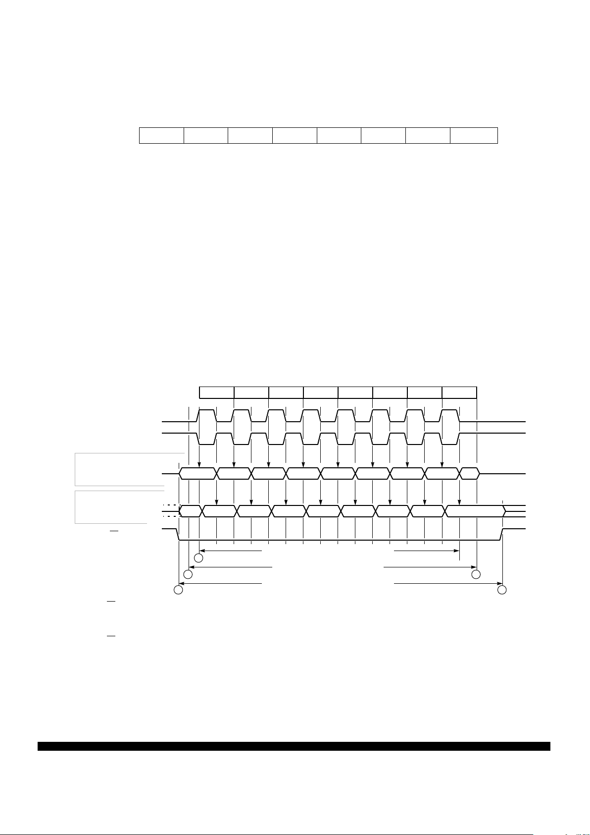
MC68HC11KA4 MOTOROLA
MC68HC11KA4TS/D 45
SPIE — Serial Peripheral Interrupt Enable
0 = SPI interrupts disabled
1 = SPI interrupts enabled
SPE — Serial Peripheral System Enable
0 = SPI off
1 = SPI on
DWOM — Port D Wired-OR Mode Option for SPI Pins PD[5:2] (See also WOMS bit in SCCR1.)
0 = Normal CMOS outputs
1 = Open-drain outputs
MSTR — Master Mode Select
0 = Slave mode
1 = Master mode
CPOL, CPHA — Clock Polarity, Clock Phase
Refer to SPI Transfer Format.
Figure 13 SPI Transfer Format
SPCR —Serial Peripheral Control Register $0028
Bit 7 654321Bit 0
SPIE SPE DWOM MSTR CPOL CPHA SPR1 SPR0
RESET: 000001UU
SPI TRANSFER FORMAT 1
23456781
SCK (CPOL = 1)
SCK (CPOL = 0)
SCK CYCLE #
SS (TO SLAVE)
654321 LSBMSB
MSB654321LSB
1
2
3
5
4
SLAVE CPHA=1 TRANSFER IN PROGRESS
MASTER TRANSFER IN PROGRESS
SLAVE CPHA=0 TRANSFER IN PROGRESS
1. SS
ASSERTED
2. MASTER WRITES TO SPDR
3. FIRST SCK EDGE
4. SPIF SET
5. SS NEGATED
SAMPLE INPUT
DATA OUT
(CPHA = 0)
SAMPLE INPUT
DATA OUT(CPHA = 1)
MOTOROLA MC68HC11KA4
46 MC68HC11KA4TS/D
NOTE
This figure shows transmission order when LSBF = 0 default. If LSBF = 1, data is
transferred in reverse order (LSB first).
SPR2, SPR1 and SPR0 — SPI Clock Rate Selects (SPR2 is located in OPT2 register)
SPIF — SPI Transfer Complete Flag
This flag is set when an SPI transfer is complete (after eight SCK cycles in a data transfer). Clear this
flag by reading SPSR (with SPIF = 1), then access SPDR data register.
0 = No SPI transfer complete or SPI transfer still in progress
1 = SPI transfer complete
WCOL — Write Collision
This flag is set if the MCU tries to write data into SPDR while an SPI data transfer is in progress. Clear
this flag by reading SPSR (WCOL = 1), then access SPDR.
0 = No write collision
1 = Write collision
Bit 5 — Not implemented
Always reads zero
MODF — Mode Fault (Mode fault terminates SPI operation)
0 = No mode fault
1 = Mode fault (SS
is pulled low while MSTR = 1)
Bits [3:0] — Not implemented
Always read zero
SPI is double buffered in, single buffered out.
SPR[2:0] Divide
E Clock By
Frequency at
E = 2 MHz (Baud)
0 0 0 2 1.0 MHz
0 0 1 4 500 kHz
0 1 0 16 125 kHz
0 1 1 32 62.5 kHz
1 0 0 8 250 kHz
1 0 1 16 125 kHz
1 1 0 64 31.3 kHz
1 1 1 128 15.6 kHz
SPSR —Serial Peripheral Status Register $0029
Bit 7 654321Bit 0
SPIF WCOL — MODF — — — —
RESET: 0000000 0
SPDR —SPI Data $002A
Bit 7 654321Bit 0
Bit 7 654321Bit 0

MC68HC11KA4 MOTOROLA
MC68HC11KA4TS/D 47
LIRDV— LIR Driven
Refer to 2 Operating Modes and On-Chip Memory.
CWOM — Port C Wired-OR Mode
Refer to 6 Parallel Input/Output.
Bit 5 — Not implemented
Always reads zero
IRVNE — Internal Read Visibility/Not E
Refer to 2 Operating Modes and On-Chip Memory.
LSBF — SPI LSB First Enable
0 = SPI data transferred MSB first
1 = SPI data transferred LSB first
SPR2 — SPI Clock (SCK) Rate Select
Adds a divide by four prescaler to SPI clock chain. Refer to SPCR register.
XDV[1:0] — XOUT Clock Divide Select
Refer to 2 Operating Modes and On-Chip Memory.
OPT2 —System Configuration Options 2 $0038
Bit 7 654321Bit 0
LIRDV CWOM — IRVNE LSBF SPR2 XDV1 XDV0
RESET: 0 0 0 — 0 0 0 0

MOTOROLA MC68HC11KA4
48 MC68HC11KA4TS/D
9 Analog-to-Digital Converter
The analog-to-digital (A/D) converter system uses an all-capacitive charge-redistribution technique to
convert analog signals to digital values. The MC68HC11KA4/KA2 A/D converter system is an 8-channel
(four channels on 64-pin version), 8-bit, multiplexed-input, successive-approximation converter. It does
not require external sample and hold circuits. The sample and hold time is 12 clock cycles. Refer to Fig-
ure 15.
The clock source for the A/D converter's charge pump, like the clock source for the EEPROM charge
pump, is selected with the CSEL bit in the OPTION register. When the E clock is slower than 1 MHz,
the CSEL bit must be set to ensure that the successive approximation sequence for the A/D converter
will be completed before any charge loss occurs. In the case of the EEPROM, it is the efficiency of the
charge pump that is affected.
Figure 14 A/D Converter Block Diagram
The A/D converter can operate in single or multiple conversion modes. Multiple conversions are performed in sequences of four. Sequences can be performed on a single channel or on a group of channels.
EA9 A/D BLOCK
PE0
AN0
PE1
AN1
PE2
AN2
PE3
AN3
PE4
AN4
PE5
AN5
PE6
AN6
PE7
AN7
ANALOG
MUX
8-BIT CAPACITIVE DAC
WITH SAMPLE AND HOLD
SUCCESSIVE APPROXIMATION
REGISTER AND CONTROL
ADCTL A/D CONTROL
CB
CC
CD
MULT
SCAN
CCF
CA
ADR1 A/D RESULT 1 ADR2 A/D RESULT 2 ADR3 A/D RESULT 3 ADR4 A/D RESULT 4
RESULT REGISTER INTERFACE
RESULT
INTERNAL
DATA BUS
V
RH
V
RL
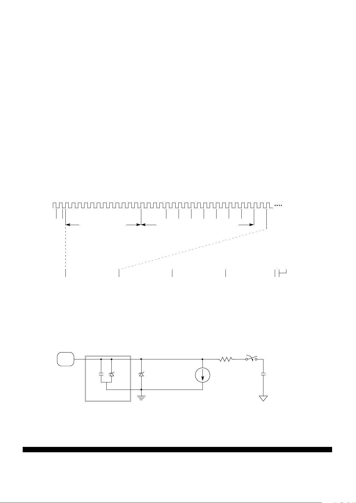
MC68HC11KA4 MOTOROLA
MC68HC11KA4TS/D 49
Pins AVDD and AVSS provide the supply voltage to the digital portion of the A/D converter. Pins VRH and
V
RL
provide the reference supply voltage inputs.
A multiplexer allows the single A/D converter to select one of 16 analog input signals. Refer to the A/D
converter channel assignment bits CD–CA description.
The A/D converter control logic implements automatic conversion sequences on a selected channel
four times or on a group of four channels once each. A write to the ADCTL register initiates conversions
and, if made while a conversion is in process, a write to ADCTL also halts a conversion operation in
progress.
When the MULT bit is zero, the A/D converter system is configured to perform four consecutive conversions on the single channel specified by the four channel-select bits (CD–CA). When the MULT bit is
one, the A/D system is configured to perform conversions on each channel in the group of four channels
specified by the CD and CC channel select bits. Refer to Table 8.
When the SCAN bit is zero, four conversions are performed in the desired channel group, once each,
to fill the four result registers. When SCAN is one, conversions continue channel-by-channel in the desired group with the result registers being updated continually as new data becomes available.
Figure 15 Timing Diagram for a Sequence of Four A/D Conversions
Figure 16 Electrical Model of an Analog Input Pin (Sample Mode)
0 32 64 96 128 — E CYCLES
SAMPLE ANALOG INPUT SUCCESSIVE APPROXIMATION SEQUENCE
MSB
4
CYCLES
BIT 6
2
CYC
BIT 5
2
CYC
BIT 4
2
CYC
BIT 3
2
CYC
BIT 2
2
CYC
BIT 1
2
CYC
LSB
2
CYC
2
CYC
END
REPEAT SEQUENCE, SCAN = 1
SET CC FLAG
CONVERT FIRST
CHANNEL, UPDATE
ADR1
CONVERT SECOND
CHANNEL, UPDATE
ADR2
CONVERT THIRD
CHANNEL, UPDATE
ADR3
CONVERT FOURTH
CHANNEL, UPDATE
ADR4
12 E CYCLES
WRITE TO ADCTL
E CLOCK
A/D CONVERSION TIM
DIFFUSION/POLY
< 2 pF
COUPLER
400 nA
JUNCTION
LEAKAGE
+ ~20V
– ~0.7V
*
* THIS ANALOG SWITCH IS CLOSED ONLY DURING THE 12-CYCLE SAMPLE TIME.
V
RL
INPUT
+ ~12V
– ~0.7V
PROTECTION
DEVICE
≤ 4 KΩ
DUMMY N-CHANNEL
OUTPUT DEVICE
ANALOG
INPUT
PIN
~ 20 pF
DAC
CAPACITANCE
ANALOG INPUT PIN

MOTOROLA MC68HC11KA4
50 MC68HC11KA4TS/D
CCF — Conversions Complete Flag
CCF is set after an A/D conversion cycle and cleared when ADCTL is written.
Bit 6 — Not implemented
Always reads zero
SCAN — Continuous Scan Control
0 = Do four conversions and stop
1 = Convert four channels in selected group continuously
MULT — Multiple Channel/Single Channel Control
0 = Convert single channel selected
1 = Convert four channels in selected group
CD–CA — Channel Select D through A
*Used for factory testing
ADCTL —A/D Control/Status $0030
Bit 7 654321Bit 0
CCF — SCAN MULT CD CC CB CA
RESET: 0000000 0
Table 8 A/D Converter Channel Assignments
Channel Select Control Bits Channel Result in ADRx if
CD CC CB CA Signal MULT = 1
0000 AN0 ADR1
0001 AN1 ADR2
0010 AN2 ADR3
0011 AN3 ADR4
0100 AN4 ADR1
0101 AN5 ADR2
0110 AN6 ADR3
0111 AN7 ADR4
1000 Reserved —
1001 Reserved —
1010 Reserved —
1011 Reserved —
1100 V
RH
* ADR1
1101 V
RL
* ADR2
1110 (V
RH
)/2* ADR3
1111 Reserved* ADR4
ADR[4:1] —A/D Results $0031–$0034
$0031 Bit 7 654321Bit 0 ADR1
$0032 Bit 7 654321Bit 0 ADR2
$0033 Bit 7 654321Bit 0 ADR3
$0034 Bit 7 654321Bit 0 ADR4

MC68HC11KA4 MOTOROLA
MC68HC11KA4TS/D 51
*Can be written only once in first 64 cycles out of reset in normal modes, any time in special mode.
ADPU — A/D Converter Power-Up
0 = A/D converter powered down
1 = A/D converter powered up
CSEL — Clock Select
0 = A/D and EEPROM use system E clock
1 = A/D and EEPROM use internal RC clock source
IRQE — IRQ Select Edge Sensitive Only
Refer to 5 Resets and Interrupts.
DLY — Enable Oscillator Start-up Delay on Exit from Stop
Refer to 5 Resets and Interrupts.
CME — Clock Monitor Enable
Refer to 5 Resets and Interrupts.
FCME — Force Clock Monitor Enable
Refer to 5 Resets and Interrupts.
CR[1:0] — COP Timer Rate Select
Refer to 5 Resets and Interrupts.
OPTION —System Configuration Options $0039
Bit 7 654321Bit 0
ADPU CSEL IRQE* DLY* CME FCME* CR1* CR0*
RESET: 0001000 0

MOTOROLA MC68HC11KA4
52 MC68HC11KA4TS/D
10 Main Timer
The timing system is based on a free-running 16-bit counter with a four-stage programmable prescaler.
A timer overflow function allows software to extend the system's timing capability beyond the counter's
16-bit range.
The timer has three channels of input capture, four channels of output compare, and one channel that
can be configured as a fourth input capture or a fifth output compare. In addition, the timing system includes pulse accumulator and real-time interrupt (RTI) functions, as well as a clock monitor function,
which can be used to detect clock failures that are not detected by the COP.
Refer to 11 Pulse Accumulator and 10.1 Real-Time Interrupt for further information about these functions. Refer to the following table for a summary of the crystal-related frequencies and periods.
Table 9 Timer Summary
XTAL Frequencies
8.0 MHz 12.0 MHz 16.0 MHz Other Rates
Control 2.0 MHz 3.0 MHz 4.0 MHz (E)
Bits 500 ns 333 ns 250 ns (1/E)
PR[1:0] Main Timer Count Rates
0 0
1 count —
overflow —
500 ns
32.768 ms
333 ns
21.845 ms
250 ns
16.384 ms
(E/1)
(E/2
16)
0 1
1 count —
overflow —
2.0 µs
131.07 ms
1.333 µs
87.381 ms
1.0 µs
65.536 ms
(E/4)
(E/2
18
)
1 0
1 count —
overflow —
4.0 µs
262.14 ms
2.667 µs
174.76 ms
2.0 µs
131.07 ms
(E/8)
(E/2
19
)
1 1
1 count —
overflow —
8.0 µs
524.29 ms
5.333 µs
349.52 ms
4.0 µs
262.14 ms
(E/16)
(E/2
20
)
RTR[1:0] Periodic (RTI) Interrupt Rates
0 0
0 1
1 0
1 1
4.096 ms
8.192 ms
16.384 ms
32.768 ms
2.731 ms
5.461 ms
10.923 ms
21.845 ms
2.048 ms
4.096 ms
8.192 ms
16.384 ms
(E/2
13)
(E/214
)
(E/2
15
)
(E/2
16
)
CR[1:0] COP Watchdog Time-out Rates
0 0
0 1
1 0
1 1
16.384 ms
65.536 ms
262.14 ms
1.049 s
10.923 ms
43.691 ms
174.76 ms
699.05 ms
8.192 ms
32.768 ms
131.07 ms
524.28 ms
(E/2
15)
(E/217
)
(E/2
19
)
(E/2
21
)
Time-out Tolerance
(–0 ms/+...) 16.4 ms 10.9 ms 8.192 ms
(E/2
15
)

MC68HC11KA4 MOTOROLA
MC68HC11KA4TS/D 53
Figure 17 Timer Block Diagram
PA3
OC5/
IC4/
OC1
16-BIT LATCH CLK
TIC1 (HI)
16-BIT COMPARATOR
=
IC3F
OC2F
OC3F
I4/O5F
TFLG1
TMSK1
IC1F
IC1I
3
IC2F
IC2I
2
IC3I
1
OC4F
I4/O5I
16-BIT TIMER BUS
16-BIT FREE-RUNNING
COUNTER
TCNT (HI)
TOF
TOI
9
PR1 PR0
PRESCALER–DIVIDE BY
1, 4, 8, OR 16
I4/O5
OC1I
8
FOC1
OC2I
7
FOC2
OC3I
6
FOC3
OC4I
5
FOC4
4
FOC5
STATUS
FLAGS
FORCE
OUTPUT
COMPARE
INTERRUPT
ENABLES
PORT A
OC5
IC4
CFORC
16-BIT TIMER BUS
OC1F
BIT-7
BIT-6
BIT-5
BIT-4
BIT-3
BIT-2
BIT-1
BIT-0
PIN
FUNCTIONS
TCNT (LO)
PA2/
IC1
TIC1 (LO)
16-BIT LATCH CLK
TIC2 (HI)
TIC2 (LO)
16-BIT LATCH CLK
TIC3 (HI)
TIC3 (LO)
TOC1 (HI) TOC1 (LO)
TOC2 (HI) TOC2 (LO)
TOC3 (HI) TOC3 (LO)
TOC4 (HI) TOC4 (LO)
16-BIT LATCH CLK
TI4/O5 (HI)
TI4/O5 (LO)
16-BIT COMPARATOR
=
16-BIT COMPARATOR
=
16-BIT COMPARATOR
=
16-BIT COMPARATOR
=
MCU
ECLK
INTERRUPT REQUESTS
(FURTHER QUALIFIED
BY I-BIT IN CCR)
PIN
CONTROL
PA7/
OC1/
PAI
PA6/
OC2/
OC1
PA5/
OC3/
OC1
PA4/
OC4/
OC1
PA1/
IC2
PA0/
IC3
TO
PULSE
ACCUMULATOR
TAPS FOR RTI, COP
WATCHDOG AND
PULSE ACCUMULATOR

MOTOROLA MC68HC11KA4
54 MC68HC11KA4TS/D
FOC[5:1] — Force Output Comparison
When the FOC bit associated with an output compare circuit is set, the output compare circuit immediately performs the action it is programmed to do when an output match occurs.
0 = Not affected
1 = Output x action occurs
Bits [2:0] — Not implemented
Always read zero
Set bit(s) to enable OC1 to control corresponding pin(s) of port A
Bits [2:0] — Not implemented
Always read zero
If OC1Mx is set, data in OC1Dx is output to port A bit x on successful OC1 compares.
Bits [2:0] — Not implemented
Always read zero
TCNT resets to $0000. In normal modes, TCNT is read-only.
TICx not affected by reset
CFORC — Timer Compare Force $000B
Bit 7 654321Bit 0
FOC1 FOC2 FOC3 FOC4 FOC5 — — —
RESET: 0000000 0
OC1M — Output Compare 1 Mask $000C
Bit 7 654321Bit 0
OC1M7 OC1M6 OC1M5 OC1M4 OC1M3 — — —
RESET: 0000000 0
OC1D — Output Compare 1 Data $000D
Bit 7 654321Bit 0
OC1D7 OC1D6 OC1D5 OC1D4 OC1D3 — — —
RESET: 0000000 0
TCNT — Timer Count $000E, $000F
$000E Bit 15 14 13 12 11 10 9 Bit 8 High TCNT
$000F Bit 7 654321Bit 0 Low
TIC1–TIC3 —Timer Input Capture $0010–$0015
$0010 Bit 15 14 13 12 11 10 9 Bit 8 High TIC1
$0011 Bit 7 654321Bit 0 Low
$0012 Bit 15 14 13 12 11 10 9 Bit 8 High TIC2
$0013 Bit 7 654321Bit 0 Low
$0014 Bit 15 14 13 12 11 10 9 Bit 8 High TIC3
$0015 Bit 7 654321Bit 0 Low

MC68HC11KA4 MOTOROLA
MC68HC11KA4TS/D 55
All TOCx register pairs reset to ones ($FFFF).
This is a shared register and is either input capture 4 or output compare 5 depending on the state of bit
I4/O5 in PACTL. Writes to TI4/O5 have no effect when this register is configured as input capture 4. All
TI4/O5 register pairs reset to ones ($FFFF).
OM[5:2] — Output Mode
OL[5:2] — Output Level
TOC1–TOC4 —Timer Output Compare $0016–$001D
$0016 Bit 15 14 13 12 11 10 9 Bit 8 High TOC1
$0017 Bit 7 654321Bit 0 Low
$0018 Bit 15 14 13 12 11 10 9 Bit 8 High TOC2
$0019 Bit 7 654321Bit 0 Low
$001A Bit 15 14 13 12 11 10 9 Bit 8 High TOC3
$001B Bit 7 654321Bit 0 Low
$001C Bit 15 14 13 12 11 10 9 Bit 8 High TOC4
$001D Bit 7 654321Bit 0 Low
TI4/O5 — Timer Input Capture 4/Output Compare 5 $001E, $001F
$001E Bit 15 14 13 12 11 10 9 Bit 8 High
$001F Bit 7 654321Bit 0 Low
TCTL1 — Timer Control 1 $0020
Bit 7 654321Bit 0
OM2 OL2 OM3 OL3 OM4 OL4 OM5 OL5
RESET: 0000000 0
OMx OLx Action Taken on Successful Compare
0 0 Timer disconnected from output pin logic
0 1 Toggle OCx output line
1 0 Clear OCx output line to 0
1 1 Set OCx output line to 1
TCTL2 — Timer Control 2 $0021
Bit 7 654321Bit 0
EDG4B EDG4A EDG1B EDG1A EDG2B EDG2A EDG3B EDG3A
RESET: 00000000

MOTOROLA MC68HC11KA4
56 MC68HC11KA4TS/D
OC1I–OC4I — Output Compare x Interrupt Enable
I4/O5I — Input Capture 4 or Output Compare 5 Interrupt Enable
IC1I–IC3I — Input Capture x Interrupt Enable
NOTE
Control bits in TMSK1 correspond bit for bit with flag bits in TFLG1. Ones in TMSK1
enable the corresponding interrupt sources.
Clear flags by writing a one to the corresponding bit position(s).
OC1F–OC4F — Output Compare x Flag
Set each time the counter matches output compare x value
I4/O5F — Input Capture 4/Output Compare 5 Flag
Set by IC4 or OC5, depending on which function was enabled by I4/O5 bit in PACTL
IC1F–IC3F — Input Capture x Flag
Set each time a selected active edge is detected on the ICx input line
TOI — Timer Overflow Interrupt Enable
0 = Timer overflow interrupt disabled
1 = Timer overflow interrupt enabled
RTII — Real-Time Interrupt Enable
0 = RTIF interrupts disabled
1 = Interrupt requested when RTIF is set to one.
Table 10 Timer Control Configuration
EDGxB EDGxA Configuration
0 0 Capture disabled
0 1 Capture on rising edges only
1 0 Capture on falling edges only
1 1 Capture on any edge
TMSK1 — Timer Interrupt Mask 1 $0022
Bit 7 654321Bit 0
OC1I OC2I OC3I OC4I I4/O5I IC1I IC2I IC3I
RESET: 0000000 0
TFLG1 — Timer Interrupt Flag 1 $0023
Bit 7 654321Bit 0
OC1F OC2F OC3F OC4F I4/O5F IC1F IC2F IC3F
RESET: 0000000 0
TMSK2 —Timer Interrupt Mask 2 $0024
Bit 7 654321Bit 0
TOI RTII PAOVI PAII — — PR1 PR0
RESET: 0000000 0

MC68HC11KA4 MOTOROLA
MC68HC11KA4TS/D 57
NOTE
Control bits [7:4] in TMSK2 correspond bit for bit with flag bits [7:4] in TFLG2. Ones
in TMSK2 enable the corresponding interrupt sources.
PAOVI — Pulse Accumulator Overflow Interrupt Enable
Refer to 11 Pulse Accumulator.
PAII — Pulse Accumulator Interrupt Enable
Refer to 11 Pulse Accumulator.
Bits [3:2] — Not implemented
Always read zero
PR[1:0] — Timer Prescaler Select
In normal modes, PR1 and PR0 can only be written once, and the write must occur within 64 cycles
after reset. Refer to 10.1 Real-Time Interrupt for specific timing values.
Clear flags by writing a one to the corresponding bit position(s).
TOF — Timer Overflow Flag
Set when TCNT changes from $FFFF to $0000
RTIF — Real-Time (Periodic) Interrupt Flag
Set periodically. Refer to RTR[1:0] bits in PACTL register.
PAOVF — Pulse Accumulator Overflow Flag
Refer to 11 Pulse Accumulator.
PAIF — Pulse Accumulator Input Edge Flag
Refer to 11 Pulse Accumulator.
Bits [3:0] — Not implemented
Always read zero
PR[1:0] Prescaler
0 0 1
0 1 4
1 0 8
1 1 16
TFLG2 — Timer Interrupt Flag 2 $0025
Bit 7 654321Bit 0
TOF RTIF PAOVF PAIF — — — —
RESET: 0000000 0

MOTOROLA MC68HC11KA4
58 MC68HC11KA4TS/D
Bit 7 — Not implemented
Always reads zero
PAEN — Pulse Accumulator System Enable
Refer to 11 Pulse Accumulator.
PAMOD — Pulse Accumulator Mode
Refer to 11 Pulse Accumulator.
PEDGE — Pulse Accumulator Edge Control
Refer to 11 Pulse Accumulator.
Bit 3 — Not implemented
Always reads zero
I4/O5 — Input Capture 4/Output Compare 5
Configure TI4/O5 for input capture or output compare
0 = OC5 enabled
1 = IC4 enabled
RTR[1:0] — Real-Time Interrupt (RTI) Rate
Refer to 10.1 Real-Time Interrupt.
10.1 Real-Time Interrupt
The real-time interrupt (RTI) function can generate interrupts at different fixed periodic rates. These
rates are a function of the MCU oscillator frequency and the value of the software-accessible control
bits, RTR1 and RTR0. These bits determine the rate at which interrupts are requested by the RTI sys-
tem. The RTI system is driven by an E divided by 2
13
rate clock compensated so that it is independent
of the timer prescaler. The RTR1 and RTR0 control bits select an additional division factor. RTI is set
to its fastest rate by default out of reset and can be changed at any time. Refer to interrupt enable and
flag bits in TMSK2 and TFLG2 registers.
PACTL —Pulse Accumulator Control $0026
Bit 7 654321Bit 0
— PAEN PAMOD PEDGE — I4/O5 RTR1 RTR0
RESET: 0000000 0
Table 11 Real-Time Interrupt Rates
RTR [1:0] Divide
E By
XTAL =
8.0 MHz
XTAL =
12.0 MHz
XTAL =
16.0 MHz
0 0
2
13
4.096 ms 2.731 ms 2.048 ms
0 1
2
14
8.192 ms 5.461 ms 4.096 ms
1 0
2
15
16.384 ms 10.923 ms 8.192 ms
1 1
2
16
32.768 ms 21.845 ms 16.384 ms
E = 2.0 MHz 3.0 MHz 4.0 MHz

MC68HC11KA4 MOTOROLA
MC68HC11KA4TS/D 59
11 Pulse Accumulator
The MC68HC11KA4/KA2 has an 8-bit counter that can be configured as a simple event counter or for
gated time accumulation. The counter can be read or written at any time.
The port A bit 7 I/O pin can be configured to act as a clock in event counting mode, or as a gate signal
to enable a free-running clock (E divided by 64) to the 8-bit counter in gated time accumulation mode.
Figure 18 Pulse Accumulator System Block Diagram
Selected Common XTAL Frequencies
Crystal 8.0 MHz 12.0 MHz 16.0 MHz
CPU Clock (E) 2.0 MHz 3.0 MHz 4.0 MHz
Cycle Time (1/E) 500 ns 333 ns 250 ns
Pulse Accumulator (Gated Mode)
(E/2
6)
1 count — 32.0 µs 21.330 µs 16.0 µs
(E/2
14
)
overflow — 8.192 ms 5.461 ms 4.096 ms
PEDGE
PAMOD
PAEN
PACTL CONTROL
INTERNAL
DATA BUS
PACNT 8-BIT COUNTER
PA7/
PAI/
OC1
INTERRUPT
REQUESTS
PAIF
PAOVF
TFLG2 INTERRUPT STATUS
PAOVI
PAII
PAOVF
PAOVI
PAIF
PAII
TMSK2 INT ENABLES
1
2
OVERFLOW
ENABLE
DISABLE
FLAG SETTING
CLOCK
PAI EDGE
PAEN
PAEN
2:1
MUX
OUTPUT
BUFFER
INPUT BUFFER
AND
EDGE DETECTOR
FROM
MAIN TIMER
OC1
DATA BUS
PIN
E ÷ 64 CLOCK
(FROM MAIN TIMER)
FROM
DDRA7

MOTOROLA MC68HC11KA4
60 MC68HC11KA4TS/D
TOI — Timer Overflow Interrupt Enable
Refer to 10 Main Timer.
RTII — Real-Time Interrupt Enable
Refer to 10 Main Timer.
PAOVI — Pulse Accumulator Overflow Interrupt Enable
0 = Pulse accumulator overflow interrupt disabled
1 = Pulse accumulator overflow interrupt enabled
PAII — Pulse Accumulator Input Interrupt Enable
0 = Pulse accumulator input interrupt disabled
1 = Pulse accumulator input interrupt enabled if PAIF bit in TFLG2 register is set
Bits [3:2] — Not implemented
Always read zero
PR[1:0] — Timer Prescaler Select
Refer to 10 Main Timer.
NOTE
Control bits [7:4] in TMSK2 correspond bit for bit with flag bits [7:4] in TFLG2. Ones
in TMSK2 enable the corresponding interrupt sources.
Clear flags by writing a one to the corresponding bit position(s).
TOF — Timer Overflow Enable
Refer to 10 Main Timer.
RTIF — Real-Time Interrupt Flag
Refer to 10 Main Timer.
PAOVF — Pulse Accumulator Overflow Flag
Set when PACNT changes from $FF to $00
PAIF — Pulse Accumulator Input Edge Flag
Set each time a selected active edge is detected on the PAI input line
Bits [3:0] — Not implemented
Always read zero
TMSK2 —Timer Interrupt Mask 2 $0024
Bit 7 654321Bit 0
TOI RTII PAOVI PAII — — PR1 PR0
RESET: 0000000 0
TFLG2 —Timer Interrupt Flag 2 $0025
Bit 7 654321Bit 0
TOF RTIF PAOVF PAIF — — — —
RESET: 0000000 0

MC68HC11KA4 MOTOROLA
MC68HC11KA4TS/D 61
Bit 7 — Not implemented
Always reads zero
PAEN — Pulse Accumulator System Enable
0 = Pulse accumulator disabled
1 = Pulse accumulator enabled
PAMOD — Pulse Accumulator Mode
0 = Event counter
1 = Gated time accumulation
PEDGE — Pulse Accumulator Edge Control
0 = In event mode, falling edges increment counter. In gated accumulation mode, high level enables
accumulator and falling edge sets PAIF.
1 = In event mode, rising edges increment counter. In gated accumulation mode, low level enables
accumulator and rising edge sets PAIF.
Bit 3 — Not implemented
Always reads zero
I4/O5 — Input Capture 4/Output Compare 5
Refer to 10 Main Timer.
RTR[1:0] — Real-Time Interrupt Rate
Refer to 10 Main Timer.
Can be read and written.
PACTL —Pulse Accumulator Control $0026
Bit 7 654321Bit 0
— PAEN PAMOD PEDGE — I4/O5 RTR1 RTR0
RESET: 0000000 0
PACNT —Pulse Accumulator Counter $0027
Bit 7 654321Bit 0
Bit 7 654321Bit 0

MOTOROLA MC68HC11KA4
62 MC68HC11KA4TS/D
12 Pulse-Width Modulation Timer
The MC68HC11KA4/KA2 MCU contains a PWM timer that is composed of a four-channel 8-bit modulator. Each of the modulators can create independent continuous waveforms with software-selectable
duty rates from 0% to 100%.
The PWM provides up to four pulse-width modulated waveforms on specific port H pins. Each channel
has its own counter. Pairs of counters can be concatenated to create 16-bit PWM outputs based on 16bit counts. Three clock sources (A, B, and S) give the PWM a wide range of frequencies.
Four control registers configure the PWM outputs — PWCLK, PWPOL, PWSCAL, and PWEN. The PWCLK register selects the prescale value for PWM clock sources and enables the 16-bit counters. The
PWPOL register determines each channel's polarity and selects the clock source for each channel. The
PWSCAL register derives a user-scaled clock, based on the A clock source, and the PWEN register
enables the PWM channels.
Each channel has a separate 8-bit counter, period register, and duty cycle register. The period and duty
cycle registers are double buffered so that if they are changed while the channel is enabled, the change
does not take effect until the counter rolls over or the channel is disabled.
With channels configured for 8-bit mode and E = 4 MHz, PWM signals of 40 kHz (1% duty cycle resolution) to less than 10 Hz (approximately 0.4% duty cycle resolution) can be produced. By configuring
the channels for 16-bit mode with E = 4 MHz, PWM periods greater than one minute are possible.
In 16-bit mode, duty cycle resolution of almost 15 parts per million can be achieved (at a PWM frequency of about 60 Hz). In the same system, a PWM frequency of 1 kHz corresponds to a duty cycle resolution of 0.025%.

MC68HC11KA4 MOTOROLA
MC68HC11KA4TS/D 63
Figure 19 Pulse Width Modulation Block Diagram
PWDTY
PWPER
PWM
OUTPUT
÷ 128
÷ 1
÷ 2
÷ 4
÷ 8
MCU
E CLOCK
SELECT
PCKB1
PCKB2
PCKB3
8-BIT COUNTER
8-BIT COMPARE
=
PWSCAL
RESET
÷ 2
CLOCK A
CLOCK S
PCLK1
PCLK2
PWEN1
PWEN2
CON12
CLOCK
SELECT
BIT 1
PWDTY1
PWCNT1 PWCNT2
8-BIT COMPARE
=
PWDTY2
PWPER2PWPER1
16-BIT
PWM
CONTROL
CON12
SRQ
CARRY
RESET
BIT 0
SRQ
MUX
PPOL1
PPOL2
÷ 32
÷ 64
CNT1 CNT2
Q
Q
MUX
÷ 16
PH0/
PW1
8-BIT COMPARE
=
8-BIT COMPARE
=
8-BIT COMPARE
=
PH1/
PW2
PORT H
PIN
CONTROL
RESET
8
88
BIT 3
PWDTY3
PWCNT3 PWCNT4
8-BIT COMPARE
=
PWDTY4
PWPER4PWPER3
16-BIT
PWM
CONTROL
CON34
SRQ
CARRY
RESET
BIT 2
SRQ
MUX
PPOL3
PPOL4
Q
Q
MUX
PH2/
PW3
8-BIT COMPARE
=
8-BIT COMPARE
=
8-BIT COMPARE
=
PH3/
PW4
RESET
88
PCLK3
PCLK4
PWEN3
PWEN4
CON34
CLOCK
SELECT
CNT3 CNT4
SELECT
CLOCK B
PCKA1 PCKA2

MOTOROLA MC68HC11KA4
64 MC68HC11KA4TS/D
CON34 —Concatenate Channels 3 and 4
Channel 3 is high-order byte, and channel 4 (port H, bit 3) is output. Clock source is determined by
PCLK4.
0 = Channels 3 and 4 are separate 8-bit PWMs.
1 = Channels 3 and 4 are concatenated to create one 16-bit PWM channel.
CON12 —Concatenate Channels One and Two
Channel 1 is high order byte, and channel 2 (port H, bit 1) is output. Clock source is determined by
PCLK2.
0 = Channels 1 and 2 are separate 8-bit PWMs
1 = Channels 1 and 2 are concatenated to create one 16-bit PWM channel.
PCKA[2:1] —Prescaler for Clock A (See also PWSCAL register)
Determines the rate of clock A
Bit 3 — Not implemented
Always reads zero
PCKB[3:1] — Prescaler for Clock B
Determines the rate for clock B
PWCLK —Pulse-Width Modulation Clock Select $0060
Bit 7 654321Bit 0
CON34 CON12 PCKA2 PCKA1 — PCKB3 PCKB2 PCKB1
RESET: 00000000
PCKA[2:1] Value of Clock A
0 0 E
0 1 E/2
1 0 E/4
1 1 E/8
PCKB[3:1] Value of Clock B
0 0 0 E
0 0 1 E/2
0 1 0 E/4
0 1 1 E/8
1 0 0 E/16
1 0 1 E/32
1 1 0 E/64
1 1 1 E/128

MC68HC11KA4 MOTOROLA
MC68HC11KA4TS/D 65
PCLK4 — Pulse-Width Channel 4 Clock Select
0 = Clock B is source
1 = Clock S is source
PCLK3 — Pulse-Width Channel 3 Clock Select
0 = Clock B is source
1 = Clock S is source
PCLK2 — Pulse-Width Channel 2 Clock Select
0 = Clock A is source
1 = Clock S is source
PCLK1 — Pulse-Width Channel 1 Clock Select
0 = Clock A is source
1 = Clock S is source
PPOL[4:1] — Pulse-Width Channel x Polarity
0 = PWM channel x output is low at the beginning of the clock cycle and goes high when duty count
is reached
1 = PWM channel x output is high at the beginning of the clock cycle and goes low when duty count
is reached
Scaled clock S is generated by dividing clock A by the value in PWSCAL, then dividing the result by 2.
If PWSCAL = $00, divide clock A by 256, then divide the result by 2.
TPWSL — PWM Scaled Clock Test Bit (TEST)
DISCP — Disable Compare Scaled E Clock (TEST)
Bits [5:4] — Not implemented
Always read zero
PWEN[1:4] — Pulse-Width Channel 1–4
0 = Channel disabled
1 = Channel enabled
PWPOL —Pulse-Width Modulation Timer Polarity $0061
Bit 7 654321Bit 0
PCLK4 PCLK3 PCLK2 PCLK1 PPOL4 PPOL3 PPOL2 PPOL1
RESET: 0000000 0
PWSCAL — Pulse-Width Modulation Timer Prescaler $0062
Bit 7 654321Bit 0
76543210
RESET: 0000000 0
PWEN — Pulse-Width Modulation Timer Enable $0063
Bit 7 654321Bit 0
TPWSL DISCP — — PWEN4 PWEN3 PWEN2 PWEN1
RESET: 0000000 0

MOTOROLA MC68HC11KA4
66 MC68HC11KA4TS/D
PWCNT[1:4]
Begins count using whichever clock was selected
PWPER[1:4]
Determines period of associated PWM channel
PWDTY[1:4]
Determines duty cycle of associated PWM channel
PWCNT[1:4] — Pulse-Width Modulation Timer Counter 1 to 4 $0064–$0067
$0064 Bit 7 654321Bit 0 PWCNT1
$0065 Bit 7 654321Bit 0 PWCNT2
$0066 Bit 7 654321Bit 0 PWCNT3
$0067 Bit 7 654321Bit 0 PWCNT4
RESET: 00000000
PWPER[1:4] —Pulse-Width Modulation Timer Period 1 to 4 $0068–$006B
$0068 Bit 7 654321Bit 0 PWPER1
$0069 Bit 7 654321Bit 0 PWPER2
$006A Bit 7 654321Bit 0 PWPER3
$006B Bit 7 654321Bit 0 PWPER4
RESET: 11111111
PWDTY[1:4] — Pulse-Width Modulation Timer Duty Cycle 1 to 4 $006C–$006F
Bit 7 654321Bit 0
$006C Bit 7 654321Bit 0 PWDTY1
$006D Bit 7 654321Bit 0 PWDTY2
$006E Bit 7 654321Bit 0 PWDTY3
$006F Bit 7 654321Bit 0 PWDTY4
RESET: 11111111

MC68HC11KA4 MOTOROLA
MC68HC11KA4TS/D 67

Motorola reserves the right to make changes without further notice to any products herein. Motorola makes no warranty, representation or guarantee regarding
the suitability of its products for any particular purpose, nor does Motorola assume any liability arising out of the application or use of any product or circuit, and
specifically disclaims any and all liability, including without limitation consequential or incidental damages. “Typical” parameters can and do vary in different
applications. All operating parameters, including “Typicals” must be validated for each customer application by customer’s technical experts. Motorola does not
convey any license under its patent rights nor the rights of others. Motorola products are not designed, intended, or authorized for use as components in
systems intended for surgical implant into the body, or other applications intended to support or sustain life, or for any other application in which the failure of
the Motorola product could create a situation where personal injury or death may occur. Should Buyer purchase or use Motorola products for any such
unintended or unauthorized application, Buyer shall indemnify and hold Motorola and its officers, employees, subsidiaries, affiliates, and distributors harmless
against all claims, costs, damages, and expenses, and reasonable attorney fees arising out of, directly or indirectly, any claim of personal injury or death
associated with such unintended or unauthorized use, even if such claim alleges that Motorola was negligent regarding the design or manufacture of the part.
Motorola and
B are registered trademarks of Motorola, Inc. Motorola, Inc. is an Equal Opportunity/Affirmative Action Employer.
How to reach us:
USA/EUROPE: Motorola Literature Distribution;
P.O. Box 20912; Phoenix, Arizona 85036. 1-800-441-2447
MFAX: RMFAX0@email.sps.mot.com - TOUCHTONE (602) 244-6609
INTERNET: http://Design-NET.com
JAPAN: Nippon Motorola Ltd.; Tatsumi-SPD-JLDC, Toshikatsu Otsuki,
6F Seibu-Butsuryu-Center, 3-14-2 Tatsumi Koto-Ku, Tokyo 135, Japan. 03-3521-8315
HONG KONG: Motorola Semiconductors H.K. Ltd.; 8B Tai Ping Industrial Park,
51 Ting Kok Road, Tai Po, N.T., Hong Kong. 852-26629298
M
 Loading...