

Datasheet MC68L11E1PB2, MC68L11E20FN2, MC68L11E20FU2, MC68L11E9B2, MC68L11E9FU2 Datasheet (Motorola)
...
M68HC11
Microcontrollers
M68HC11E Family
Technical Data
M68HC11E/D
Rev. 4, 7/2002
WWW.MOTOROLA.COM/SEMICONDUCTORS

MC68HC11E Family
Technical Data
To provide the most up-to-date information, the revision of our
documents on the World Wide Web will be the most current. Your printed
copy may b e an earlier revision. To ve rify you have the latest information
available, refer to:
http://www.motorola.com/semiconductors/
The following revision history table summarizes changes contained in
this document. For your convenience, the page number designators
have been linked to the appropriate location.
Motorola and the Stylized M Logo are registered trademarks of Motorola, Inc.
DigitalDNA is a trademark of Motorola, Inc. © Motorola, Inc., 2002
0&+&()DPLO\²5HY
027252/$
7HFKQLFDO'DWD

5HYLVLRQ+LVWRU\
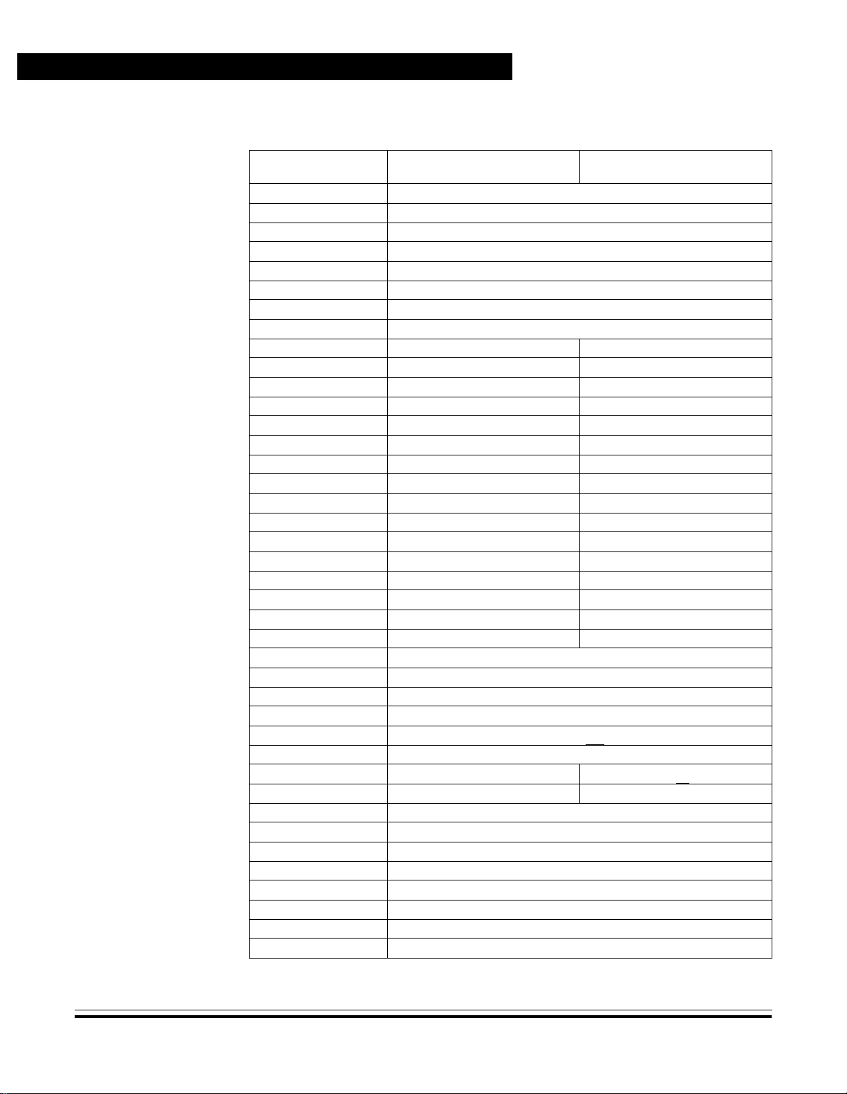
Revision History
Date
May, 2001 3.1
June, 2001 3.2
December,
2001
July, 2002 4
Revision
Level
3.3
Description
4.4.3.1 System Configuration Register — Addition to NOCOP bit
description
Added 11.22 EPROM Characteristics 251
11.22 EPROM Characteristics — For clarity, addition to note 2
following the table
7.8.2 Serial Communications Control Register 1 — SCCR1 bit 4
(M) description corrected
11.8 MC68L11E9/E20 DC Electrical Characteristics — Title
changed to include the MC68L11E20
11.9 MC68L11E9/E20 Supply Currents and Power Dissipation —
Title changed to include the MC68L11E2 0
11.11 MC68L11E9/E20 Control Timing — Title changed to include
the MC68L11E20
11.13 MC68L11E9/E20 Pe ripher al Port Timin g — Title changed to
include the MC68L1 1E20
11.15 MC68L11E9/E20 Analog-to-Digital Converter
Characteristics — Title changed to include the MC68L11E20
11.17 MC68L11E9/E20 Expansio n Bus Timing Characteristics —
Title changed to include the MC68L11E2 0
Page
Number(s)
88
251
153
226
227
230
236
241
244
11.19 MC68L11E9/E20 Serial Peirpheral Interface Characteristics
— Title changed to include the MC68L11E20
11.21 MC68L11E9/E20 EEPROM Char acteri stics — Title changed
to include the MC68L11E20
13.5 Extended Voltage Device Ordering Information (3.0 Vdc to
5.5 Vdc) — Updated table to include MC68L1120
7HFKQLFDO'DWD 0&+&()DPLO\²5HY
247
250
267
027252/$

Technical Data — M68HC11E Family
Section 1. General Description . . . . . . . . . . . . . . . . . . . .23
Section 2. Pin Descriptions . . . . . . . . . . . . . . . . . . . . . . .27
Section 3. Central Processor Unit (CPU) . . . . . . . . . . . .45
Section 4. Operating Modes and On-Chip Memory . . . .65
Section 5. Resets and Interrupts . . . . . . . . . . . . . . . . . .107
Section 6. Parallel Input/Output (I/O) Ports . . . . . . . . .133
List of Sections
Section 7. Serial Communications Interface (SCI). . . .145
Section 8. Serial Peripheral Interface (SPI). . . . . . . . . .165
Section 9. Timing System. . . . . . . . . . . . . . . . . . . . . . . .177
Section 10. Analog-to-Digital (A/D) Converter . . . . . . .209
Section 11. Electrical Characteristics . . . . . . . . . . . . . .221
Section 12. Mechanical Data . . . . . . . . . . . . . . . . . . . . .253
Section 13. Ordering Information . . . . . . . . . . . . . . . . .261
Appendix A. Development Support. . . . . . . . . . . . . . . .269
Appendix B. EVBU Schematic . . . . . . . . . . . . . . . . . . . .275
MC68HC11E Family — Rev. 4 Technical Data
MOTOROLA List of Sections 5

List of Sec ti o ns
AN1060 — M68HC11 Bootstrap Mode . . . . . . . . . . . . .277
EB184 — Enabling the Secu rity Feature
on the MC68HC711E9 Devices with PCbug11
on the M68HC711E9PGMR . . . . . . . . . . . . . . . . . . . 323
EB188 — Enabling the Secu rity Feature
on M68H C811E2 Devi ces with PCbug11
on the M68HC711E9PGMR . . . . . . . . . . . . . . . . . . . 327
EB296 — Programming MC68HC711E9 Devices
with PCbug11 and the M68HC11EVBU . . . . . . . . . 331
Technical Data MC68HC11E Family — Rev. 4
6 List of Sections MOTOROLA

Technical Data — M68HC11E Family
Section 1. General Description
1.1 Contents. . . . . . . . . . . . . . . . . . . . . . . . . . . . . . . . . . . . . . . . . .23
1.2 Introduction. . . . . . . . . . . . . . . . . . . . . . . . . . . . . . . . . . . . . . . .23
1.3 Features . . . . . . . . . . . . . . . . . . . . . . . . . . . . . . . . . . . . . . . . . .24
1.4 Structure. . . . . . . . . . . . . . . . . . . . . . . . . . . . . . . . . . . . . . . . . .25
Section 2. Pin Descriptions
2.1 Contents. . . . . . . . . . . . . . . . . . . . . . . . . . . . . . . . . . . . . . . . . .27
2.2 Introduction. . . . . . . . . . . . . . . . . . . . . . . . . . . . . . . . . . . . . . . .28
Table of Contents
2.3 V
2.4 RESET
2.5 Crystal Driver and External Clock Input
2.6 E-Clock Output (E) . . . . . . . . . . . . . . . . . . . . . . . . . . . . . . . . . .36
2.7 Interrupt Request (IRQ
2.8 Non-Maskable Interrupt (XIRQ
2.9 MODA and MODB (MODA/LIR and MODB/V
2.10 VRL and VRH. . . . . . . . . . . . . . . . . . . . . . . . . . . . . . . . . . . . . . .38
2.11 STRA/AS . . . . . . . . . . . . . . . . . . . . . . . . . . . . . . . . . . . . . . . . .38
2.12 STRB/R/W . . . . . . . . . . . . . . . . . . . . . . . . . . . . . . . . . . . . . . . .38
2.13 Port Signals . . . . . . . . . . . . . . . . . . . . . . . . . . . . . . . . . . . . . . .39
2.13.1 Port A . . . . . . . . . . . . . . . . . . . . . . . . . . . . . . . . . . . . . . . . . .39
2.13.2 Port B . . . . . . . . . . . . . . . . . . . . . . . . . . . . . . . . . . . . . . . . . .41
2.13.3 Port C. . . . . . . . . . . . . . . . . . . . . . . . . . . . . . . . . . . . . . . . . .42
2.13.4 Port D. . . . . . . . . . . . . . . . . . . . . . . . . . . . . . . . . . . . . . . . . .43
2.13.5 Port E . . . . . . . . . . . . . . . . . . . . . . . . . . . . . . . . . . . . . . . . . .43
and VSS. . . . . . . . . . . . . . . . . . . . . . . . . . . . . . . . . . . . . . .32
DD
. . . . . . . . . . . . . . . . . . . . . . . . . . . . . . . . . . . . . . . . . . .34
(XTAL and EXTAL) . . . . . . . . . . . . . . . . . . . . . . . . . . . . . . .35
) . . . . . . . . . . . . . . . . . . . . . . . . . . . . . .36
/V
). . . . . . . . . . . . . . . . . . . .36
PPE
) . . . . . . . . .37
STBY
MC68HC11E Family — Rev. 4 Technical Data
MOTOROLA Table of Contents 7

Table of Contents
Section 3. Central Processor Unit (CPU)
3.1 Contents. . . . . . . . . . . . . . . . . . . . . . . . . . . . . . . . . . . . . . . . . .45
3.2 Introduction. . . . . . . . . . . . . . . . . . . . . . . . . . . . . . . . . . . . . . . .46
3.3 CPU Registers . . . . . . . . . . . . . . . . . . . . . . . . . . . . . . . . . . . . .46
3.3.1 Accumulators A, B, and D . . . . . . . . . . . . . . . . . . . . . . . . . .4 7
3.3.2 Index Register X (IX) . . . . . . . . . . . . . . . . . . . . . . . . . . . . . .48
3.3.3 Index Register Y (IY) . . . . . . . . . . . . . . . . . . . . . . . . . . . . . .48
3.3.4 Stack Pointer (SP) . . . . . . . . . . . . . . . . . . . . . . . . . . . . . . . .48
3.3.5 Program Counter (PC) . . . . . . . . . . . . . . . . . . . . . . . . . . . . .50
3.3.6 Condition Code Register (CCR). . . . . . . . . . . . . . . . . . . . . .51
3.3.6.1 Carry/Borrow (C) . . . . . . . . . . . . . . . . . . . . . . . . . . . . . . .51
3.3.6.2 Overflow (V). . . . . . . . . . . . . . . . . . . . . . . . . . . . . . . . . . .51
3.3.6.3 Zero (Z) . . . . . . . . . . . . . . . . . . . . . . . . . . . . . . . . . . . . . .51
3.3.6.4 Negative (N). . . . . . . . . . . . . . . . . . . . . . . . . . . . . . . . . . .52
3.3.6.5 Interrupt Mask (I) . . . . . . . . . . . . . . . . . . . . . . . . . . . . . . .52
3.3.6.6 Half Carry (H). . . . . . . . . . . . . . . . . . . . . . . . . . . . . . . . . .52
3.3.6.7 X Interrupt Mask (X). . . . . . . . . . . . . . . . . . . . . . . . . . . . .52
3.3.6.8 STOP Disable (S) . . . . . . . . . . . . . . . . . . . . . . . . . . . . . .53
3.4 Data Types. . . . . . . . . . . . . . . . . . . . . . . . . . . . . . . . . . . . . . . .53
3.5 Opcodes and Operands . . . . . . . . . . . . . . . . . . . . . . . . . . . . . .5 3
3.6 Addressing Modes . . . . . . . . . . . . . . . . . . . . . . . . . . . . . . . . . . 5 4
3.6.1 Immediate. . . . . . . . . . . . . . . . . . . . . . . . . . . . . . . . . . . . . . .54
3.6.2 Direct . . . . . . . . . . . . . . . . . . . . . . . . . . . . . . . . . . . . . . . . . .55
3.6.3 Extended . . . . . . . . . . . . . . . . . . . . . . . . . . . . . . . . . . . . . . . 5 5
3.6.4 Indexed. . . . . . . . . . . . . . . . . . . . . . . . . . . . . . . . . . . . . . . . .55
3.6.5 Inherent . . . . . . . . . . . . . . . . . . . . . . . . . . . . . . . . . . . . . . . .55
3.6.6 Relative . . . . . . . . . . . . . . . . . . . . . . . . . . . . . . . . . . . . . . . .56
3.7 Instruction Set. . . . . . . . . . . . . . . . . . . . . . . . . . . . . . . . . . . . . .56
Technical Data MC68HC11E Family — Rev. 4
8 Table of Contents M OTOROLA

Table of Contents
Section 4. Operating Modes and On-Chip Memory
4.1 Contents. . . . . . . . . . . . . . . . . . . . . . . . . . . . . . . . . . . . . . . . . .65
4.2 Introduction. . . . . . . . . . . . . . . . . . . . . . . . . . . . . . . . . . . . . . . .66
4.3 Operating Modes . . . . . . . . . . . . . . . . . . . . . . . . . . . . . . . . . . .66
4.3.1 Single-Chip Mode. . . . . . . . . . . . . . . . . . . . . . . . . . . . . . . . .66
4.3.2 Expanded Mode. . . . . . . . . . . . . . . . . . . . . . . . . . . . . . . . . .67
4.3.3 Test Mode . . . . . . . . . . . . . . . . . . . . . . . . . . . . . . . . . . . . . .67
4.3.4 Bootstrap Mode . . . . . . . . . . . . . . . . . . . . . . . . . . . . . . . . . .68
4.4 Memory Map. . . . . . . . . . . . . . . . . . . . . . . . . . . . . . . . . . . . . . .6 9
4.4.1 RAM and Input/Output Mapping. . . . . . . . . . . . . . . . . . . . . .80
4.4.2 Mode Selection. . . . . . . . . . . . . . . . . . . . . . . . . . . . . . . . . . .82
4.4.3 System Initialization . . . . . . . . . . . . . . . . . . . . . . . . . . . . . . .85
4.4.3.1 System Configuration Register . . . . . . . . . . . . . . . . . . . .86
4.4.3.2 RAM and I/O Mapping Register . . . . . . . . . . . . . . . . . . . .89
4.4.3.3 System Configuration Options Register. . . . . . . . . . . . . .91
4.5 EPROM/OTPROM . . . . . . . . . . . . . . . . . . . . . . . . . . . . . . . . . .92
4.5.1 Programming an Individual EPROM Address . . . . . . . . . . .93
4.5.2 Programming the EPROM with Downloaded Data. . . . . . . .94
4.5.3 EPROM and EEPROM Programming
Control Register . . . . . . . . . . . . . . . . . . . . . . . . . . . . . . .94
4.6 EEPROM . . . . . . . . . . . . . . . . . . . . . . . . . . . . . . . . . . . . . . . . .98
4.6.1 EEPROM and CONFIG Programming and Erasure. . . . . . .98
4.6.1.1 Block Protect Register . . . . . . . . . . . . . . . . . . . . . . . . . . .9 9
4.6.1.2 EPROM and EEPROM Programming
Control Register . . . . . . . . . . . . . . . . . . . . . . . . . . . .101
4.6.1.3 EEPROM Bulk Erase. . . . . . . . . . . . . . . . . . . . . . . . . . .103
4.6.1.4 EEPROM Row Erase. . . . . . . . . . . . . . . . . . . . . . . . . . .103
4.6.1.5 EEPROM Byte Erase. . . . . . . . . . . . . . . . . . . . . . . . . . .104
4.6.1.6 CONFIG Register Programming . . . . . . . . . . . . . . . . . .104
4.6.2 EEPROM Security . . . . . . . . . . . . . . . . . . . . . . . . . . . . . . .104
MC68HC11E Family — Rev. 4 Technical Data
MOTOROLA Table of Contents 9

Table of Contents
Section 5. Resets and Interrupts
5.1 Contents. . . . . . . . . . . . . . . . . . . . . . . . . . . . . . . . . . . . . . . . .107
5.2 Introduction. . . . . . . . . . . . . . . . . . . . . . . . . . . . . . . . . . . . . . .108
5.3 Resets. . . . . . . . . . . . . . . . . . . . . . . . . . . . . . . . . . . . . . . . . . .108
5.3.1 Power-On Reset (POR) . . . . . . . . . . . . . . . . . . . . . . . . . . .109
5.3.2 External Reset (RESET) . . . . . . . . . . . . . . . . . . . . . . . . . .109
5.3.3 Computer Operating Properly (COP) Reset. . . . . . . . . . . .110
5.3.4 Clock Monitor Reset. . . . . . . . . . . . . . . . . . . . . . . . . . . . . .111
5.3.5 System Configuration Options Register . . . . . . . . . . . . . . .112
5.3.6 Configuration Control Register. . . . . . . . . . . . . . . . . . . . . .113
5.4 Effects of Reset . . . . . . . . . . . . . . . . . . . . . . . . . . . . . . . . . . .114
5.4.1 Central Processor Unit (CPU) . . . . . . . . . . . . . . . . . . . . . .115
5.4.2 Memory Map . . . . . . . . . . . . . . . . . . . . . . . . . . . . . . . . . . .115
5.4.3 Timer . . . . . . . . . . . . . . . . . . . . . . . . . . . . . . . . . . . . . . . . .115
5.4.4 Real-Time Interrupt (RTI) . . . . . . . . . . . . . . . . . . . . . . . . . .116
5.4.5 Pulse Accumulator . . . . . . . . . . . . . . . . . . . . . . . . . . . . . . .116
5.4.6 Computer Operating Properly (COP). . . . . . . . . . . . . . . . .116
5.4.7 Serial Communications Interface (SCI) . . . . . . . . . . . . . . .116
5.4.8 Serial Peripheral Interface (SPI). . . . . . . . . . . . . . . . . . . . .117
5.4.9 Analog-to-Digital (A/D) Converter. . . . . . . . . . . . . . . . . . . .117
5.4.10 System . . . . . . . . . . . . . . . . . . . . . . . . . . . . . . . . . . . . . . . .117
5.5 Reset and Interrupt Priority. . . . . . . . . . . . . . . . . . . . . . . . . . .117
5.5.1 Highest Priority Interrupt and Miscellaneous Register. . . .119
5.6 Interrupts. . . . . . . . . . . . . . . . . . . . . . . . . . . . . . . . . . . . . . . . .121
5.6.1 Interrupt Recognition and Register Stacking . . . . . . . . . . .122
5.6.2 Non-Maskable Interrupt Request (XIRQ). . . . . . . . . . . . . .123
5.6.3 Illegal Opcode Trap . . . . . . . . . . . . . . . . . . . . . . . . . . . . . .123
5.6.4 Software Interrupt (SWI). . . . . . . . . . . . . . . . . . . . . . . . . . .124
5.6.5 Maskable Interrupts . . . . . . . . . . . . . . . . . . . . . . . . . . . . . .124
5.6.6 Reset and Interrupt Processing . . . . . . . . . . . . . . . . . . . . .124
5.7 Low-Power Operation. . . . . . . . . . . . . . . . . . . . . . . . . . . . . . .129
5.7.1 Wait Mode . . . . . . . . . . . . . . . . . . . . . . . . . . . . . . . . . . . . .130
5.7.2 Stop Mode . . . . . . . . . . . . . . . . . . . . . . . . . . . . . . . . . . . . .130
Technical Data MC68HC11E Family — Rev. 4
10 Table of Contents M OTOROLA

Table of Contents
Section 6. Parallel Input/Output (I/O) Ports
6.1 Contents. . . . . . . . . . . . . . . . . . . . . . . . . . . . . . . . . . . . . . . . .133
6.2 Introduction. . . . . . . . . . . . . . . . . . . . . . . . . . . . . . . . . . . . . . .133
6.3 Port A . . . . . . . . . . . . . . . . . . . . . . . . . . . . . . . . . . . . . . . . . . .134
6.4 Port B . . . . . . . . . . . . . . . . . . . . . . . . . . . . . . . . . . . . . . . . . . .136
6.5 Port C . . . . . . . . . . . . . . . . . . . . . . . . . . . . . . . . . . . . . . . . . . .136
6.6 Port D . . . . . . . . . . . . . . . . . . . . . . . . . . . . . . . . . . . . . . . . . . .138
6.7 Port E . . . . . . . . . . . . . . . . . . . . . . . . . . . . . . . . . . . . . . . . . . .139
6.8 Handshake Protocol. . . . . . . . . . . . . . . . . . . . . . . . . . . . . . . .139
6.9 Parallel I/O Control Register. . . . . . . . . . . . . . . . . . . . . . . . . .141
Section 7. S e ri al Com m uni c at ion s Int er fa ce (SCI)
7.1 Contents. . . . . . . . . . . . . . . . . . . . . . . . . . . . . . . . . . . . . . . . .145
7.2 Introduction. . . . . . . . . . . . . . . . . . . . . . . . . . . . . . . . . . . . . . .145
7.3 Data Format . . . . . . . . . . . . . . . . . . . . . . . . . . . . . . . . . . . . . .146
7.4 Transmit Operation. . . . . . . . . . . . . . . . . . . . . . . . . . . . . . . . .146
7.5 Receive Operation . . . . . . . . . . . . . . . . . . . . . . . . . . . . . . . . .148
7.6 Wakeup Feature. . . . . . . . . . . . . . . . . . . . . . . . . . . . . . . . . . .148
7.6.1 Idle-Line Wakeup. . . . . . . . . . . . . . . . . . . . . . . . . . . . . . . .150
7.6.2 Address-Mark Wakeup. . . . . . . . . . . . . . . . . . . . . . . . . . . .150
7.7 SCI Error Detection. . . . . . . . . . . . . . . . . . . . . . . . . . . . . . . . .151
7.8 SCI Registers . . . . . . . . . . . . . . . . . . . . . . . . . . . . . . . . . . . . .152
7.8.1 Serial Communications Data Register . . . . . . . . . . . . . . . .152
7.8.2 Serial Communications Control Register 1 . . . . . . . . . . . .153
7.8.3 Serial Communications Control Register 2 . . . . . . . . . . . .154
7.8.4 Serial Communication Status Register. . . . . . . . . . . . . . . .155
7.8.5 Baud Rate Register . . . . . . . . . . . . . . . . . . . . . . . . . . . . . .157
7.9 Status Flags and Interrupts. . . . . . . . . . . . . . . . . . . . . . . . . . .160
7.10 Receiver Flags . . . . . . . . . . . . . . . . . . . . . . . . . . . . . . . . . . . .162
MC68HC11E Family — Rev. 4 Technical Data
MOTOROLA Table of Contents 11

Table of Contents
Section 8. Serial Peripheral Interface (SPI)
8.1 Contents. . . . . . . . . . . . . . . . . . . . . . . . . . . . . . . . . . . . . . . . .165
8.2 Introduction. . . . . . . . . . . . . . . . . . . . . . . . . . . . . . . . . . . . . . .166
8.3 Functional Description . . . . . . . . . . . . . . . . . . . . . . . . . . . . . .166
8.4 SPI Transfer Formats . . . . . . . . . . . . . . . . . . . . . . . . . . . . . . .168
8.5 Clock Phase and Polarity Controls . . . . . . . . . . . . . . . . . . . . .169
8.6 SPI Signals. . . . . . . . . . . . . . . . . . . . . . . . . . . . . . . . . . . . . . .169
8.6.1 Master In/Slave Out . . . . . . . . . . . . . . . . . . . . . . . . . . . . . .170
8.6.2 Master Out/Slave In . . . . . . . . . . . . . . . . . . . . . . . . . . . . . .170
8.6.3 Serial Clock . . . . . . . . . . . . . . . . . . . . . . . . . . . . . . . . . . . .170
8.6.4 Slave Select . . . . . . . . . . . . . . . . . . . . . . . . . . . . . . . . . . . .170
8.7 SPI System Errors . . . . . . . . . . . . . . . . . . . . . . . . . . . . . . . . .171
8.8 SPI Registers . . . . . . . . . . . . . . . . . . . . . . . . . . . . . . . . . . . . .172
8.8.1 Serial Peripheral Control Register . . . . . . . . . . . . . . . . . .173
8.8.2 Serial Peripheral Status Register . . . . . . . . . . . . . . . . . . .175
8.8.3 Serial Peripheral Data I/O Register . . . . . . . . . . . . . . . . . . 176
Section 9. Timing System
9.1 Contents. . . . . . . . . . . . . . . . . . . . . . . . . . . . . . . . . . . . . . . . .177
9.2 Introduction. . . . . . . . . . . . . . . . . . . . . . . . . . . . . . . . . . . . . . .178
9.3 Timer Structure. . . . . . . . . . . . . . . . . . . . . . . . . . . . . . . . . . . .180
9.4 Input Capture . . . . . . . . . . . . . . . . . . . . . . . . . . . . . . . . . . . . .182
9.4.1 Timer Control Register 2 . . . . . . . . . . . . . . . . . . . . . . . . . .183
9.4.2 Timer Input Capture Registers. . . . . . . . . . . . . . . . . . . . . .184
9.4.3 Timer Input Capture 4/Output Compare 5 Register. . . . . .186
9.5 Output Compare. . . . . . . . . . . . . . . . . . . . . . . . . . . . . . . . . . .186
9.5.1 Timer Output Compare Registers . . . . . . . . . . . . . . . . . . .187
9.5.2 Timer Compare Force Register . . . . . . . . . . . . . . . . . . . . .190
9.5.3 Output Compare Mask Register. . . . . . . . . . . . . . . . . . . . .191
9.5.4 Output Compare Data Register . . . . . . . . . . . . . . . . . . . . .192
9.5.5 Timer Counter Register . . . . . . . . . . . . . . . . . . . . . . . . . . .193
9.5.6 Timer Control Register 1 . . . . . . . . . . . . . . . . . . . . . . . . . .194
9.5.7 Timer Interrupt Mask 1 Register. . . . . . . . . . . . . . . . . . . . .195
9.5.8 Timer Interrupt Flag 1 Register . . . . . . . . . . . . . . . . . . . . .196
Technical Data MC68HC11E Family — Rev. 4
12 Table of Contents M OTOROLA

Table of Contents
9.5.9 Timer Interrupt Mask 2 Register. . . . . . . . . . . . . . . . . . . . .196
9.5.10 Timer Interrupt Flag Register 2 . . . . . . . . . . . . . . . . . . . . .198
9.6 Real-Time Interrupt (RTI) . . . . . . . . . . . . . . . . . . . . . . . . . . . .199
9.6.1 Timer Interrupt Mask Register 2. . . . . . . . . . . . . . . . . . . . .200
9.6.2 Timer Interrupt Flag Register 2 . . . . . . . . . . . . . . . . . . . . .201
9.6.3 Pulse Accumulator Control Register . . . . . . . . . . . . . . . . .202
9.7 Computer Operating Properly (COP) Watchdog Function . . .203
9.8 Pulse Accumulator . . . . . . . . . . . . . . . . . . . . . . . . . . . . . . . . .203
9.8.1 Pulse Accumulator Control Register . . . . . . . . . . . . . . . . .205
9.8.2 Pulse Accumulator Count Register . . . . . . . . . . . . . . . . . .206
9.8.3 Pulse Accumulator Status and Interrupt Bits . . . . . . . . . . .207
Section 10. Analog-to-Digital (A/D) Converter
10.1 Contents. . . . . . . . . . . . . . . . . . . . . . . . . . . . . . . . . . . . . . . . .209
10.2 Introduction. . . . . . . . . . . . . . . . . . . . . . . . . . . . . . . . . . . . . . .209
10.3 Overview. . . . . . . . . . . . . . . . . . . . . . . . . . . . . . . . . . . . . . . . .210
10.3.1 Multiplexer . . . . . . . . . . . . . . . . . . . . . . . . . . . . . . . . . . . . .210
10.3.2 Analog Converter. . . . . . . . . . . . . . . . . . . . . . . . . . . . . . . .212
10.3.3 Digital Control. . . . . . . . . . . . . . . . . . . . . . . . . . . . . . . . . . .212
10.3.4 Result Registers. . . . . . . . . . . . . . . . . . . . . . . . . . . . . . . . .212
10.3.5 A/D Converter Clocks. . . . . . . . . . . . . . . . . . . . . . . . . . . . .213
10.3.6 Conversion Sequence . . . . . . . . . . . . . . . . . . . . . . . . . . . .213
10.4 A/D Converter Power-Up and Clock Select . . . . . . . . . . . . . .214
10.5 Conversion Process . . . . . . . . . . . . . . . . . . . . . . . . . . . . . . . .215
10.6 Channel Assignments. . . . . . . . . . . . . . . . . . . . . . . . . . . . . . .216
10.7 Single-Channel Operation . . . . . . . . . . . . . . . . . . . . . . . . . . .216
10.8 Multiple-Channel Operation . . . . . . . . . . . . . . . . . . . . . . . . . .217
10.9 Operation in Stop and Wait Modes. . . . . . . . . . . . . . . . . . . . .217
10.10 A/D Control/Status Register . . . . . . . . . . . . . . . . . . . . . . . . . . 218
10.11 A/D Converter Result Registers . . . . . . . . . . . . . . . . . . . . . . .220
MC68HC11E Family — Rev. 4 Technical Data
MOTOROLA Table of Contents 13

Table of Contents
Section 11. Electrical Characteristics
11.1 Contents. . . . . . . . . . . . . . . . . . . . . . . . . . . . . . . . . . . . . . . . .221
11.2 Introduction. . . . . . . . . . . . . . . . . . . . . . . . . . . . . . . . . . . . . . .222
11.3 Maximum Ratings for Standard
and Extended Voltage Devices . . . . . . . . . . . . . . . . . . . . .222
11.4 Functional Operating Range. . . . . . . . . . . . . . . . . . . . . . . . . .223
11.5 Thermal Characteristics . . . . . . . . . . . . . . . . . . . . . . . . . . . . .223
11.6 DC Electrical Characteristics . . . . . . . . . . . . . . . . . . . . . . . . .224
11.7 Supply Currents and Power Dissipation. . . . . . . . . . . . . . . . .225
11.8 MC68L11E9/E20 DC Electrical Characteristics . . . . . . . . . . .226
11.9 MC68L11E9/E20 Supply Currents and Power Dissipation. . .227
11.10 Control Timing . . . . . . . . . . . . . . . . . . . . . . . . . . . . . . . . . . . .229
11.11 MC68L11E9/E20 Control Timing . . . . . . . . . . . . . . . . . . . . . .230
11.12 Peripheral Port Timing . . . . . . . . . . . . . . . . . . . . . . . . . . . . . .235
11.13 MC68L11E9/E20 Peripheral Port Timing . . . . . . . . . . . . . . . .236
11.14 Analog-to-Digital Converter Characteristics . . . . . . . . . . . . . .240
11.15 MC68L11E9/E20 Analog-to-Digital
Converter Characteristics . . . . . . . . . . . . . . . . . . . . . . . . .241
11.16 Expansion Bus Timing Characteristics. . . . . . . . . . . . . . . . . .242
11.17 MC68L11E9/E20 Expansion Bus Timing Characteristics. . . .244
11.18 Serial Peripheral Interface Timing Characteristics . . . . . . . . .246
11.19 MC68L11E9/E20 Serial Peirpheral
Interface Characteristics . . . . . . . . . . . . . . . . . . . . . . . . . .247
11.20 EEPROM Characteristics . . . . . . . . . . . . . . . . . . . . . . . . . . .250
11.21 MC68L11E9/E20 E EPROM Characteristics. . . . . . . . . . . . . .250
11.22 EPROM Characteristics . . . . . . . . . . . . . . . . . . . . . . . . . . . . .251
Technical Data MC68HC11E Family — Rev. 4
14 Table of Contents M OTOROLA

Table of Contents
Section 12. Mechanical Data
12.1 Contents. . . . . . . . . . . . . . . . . . . . . . . . . . . . . . . . . . . . . . . . .253
12.2 Introduction. . . . . . . . . . . . . . . . . . . . . . . . . . . . . . . . . . . . . . .253
12.3 52-Pin Plastic-Leaded Chip Carrier (Case 778) . . . . . . . . . . .254
12.4 52-Pin Windowed Ceramic-Leaded
Chip Carrier (Case 778B) . . . . . . . . . . . . . . . . . . . . . . . . .255
12.5 64-Pin Quad Flat P a ck (Case 840C) . . . . . . . . . . . . . . . . . . .256
12.6 52-Pin Thin Quad Flat Pack (Case 848D) . . . . . . . . . . . . . . .257
12.7 56-Pin Dual in-Line Package (Case #859) . . . . . . . . . . . . . . .258
12.8 48-Pin Plastic DIP (Case 767) . . . . . . . . . . . . . . . . . . . . . . . .259
Section 13. Ordering Information
13.1 Contents. . . . . . . . . . . . . . . . . . . . . . . . . . . . . . . . . . . . . . . . .261
13.2 Introduction. . . . . . . . . . . . . . . . . . . . . . . . . . . . . . . . . . . . . . .261
13.3 Standard Device Ordering Information. . . . . . . . . . . . . . . . . .262
13.4 Custom ROM Device Ordering Information . . . . . . . . . . . . . .265
13.5 Extended Voltage Device Ordering Information
(3.0 Vdc to 5.5 Vdc). . . . . . . . . . . . . . . . . . . . . . . . . . . . . .267
Appendix A. Development Support
A.1 Contents. . . . . . . . . . . . . . . . . . . . . . . . . . . . . . . . . . . . . . . . .269
A.2 Introduction. . . . . . . . . . . . . . . . . . . . . . . . . . . . . . . . . . . . . . .269
A.3 Motorola M68HC11 E-Series Development Tools . . . . . . . . .270
A.4 EVS — Evaluation System. . . . . . . . . . . . . . . . . . . . . . . . . . .270
A.5 Motorola Modular Development System (MMDS11) . . . . . . .271
A.6 SPGMR11 — Serial Programmer for M68HC11 MCUs . . . . .273
Appendi x B . EVBU Schematic
M68HC11EVBU Schematic. . . . . . . . . . . . . . . . . . . . . . . . . . . . . . . .275
MC68HC11E Family — Rev. 4 Technical Data
MOTOROLA Table of Contents 15

Table of Contents
AN1060
AN1060 — M68HC11 Bootstrap Mode . . . . . . . . . . . . . . . . . . . . . . 277
EB184
EB184 — Enabling the Security Feature on the MC68HC711E9
Devices with PCbug11 on the M68HC711E9PGMR 323
EB188
EB188 — Enabling the Security Feature on M68HC811E2
Devices with PCbug11 on the M68HC711E9PGMR . . . . . . . . . 327
EB296
EB296 — Programming MC68HC711E9 Devices
with PCbug11 and the M68HC11EVBU. . . . . . . . . . . . . . . . . . . 331
Technical Data MC68HC11E Family — Rev. 4
16 Table of Contents M OTOROLA

Technical Data — M68HC11E Family
Figure Title P age
1-1 M68HC11 E-Series Block Diagram . . . . . . . . . . . . . . . . . . . .26
2-1 Pin Assignments for 52-Pin PLCC and CLCC . . . . . . . . . . . .28
2-2 Pin Assignments for 64-Pin QFP . . . . . . . . . . . . . . . . . . . . . .29
2-3 Pin Assignments for 52-Pin TQFP . . . . . . . . . . . . . . . . . . . . .3 0
2-4 Pin Assignments for 56-Pin SDIP. . . . . . . . . . . . . . . . . . . . . .31
2-5 Pin Assignments for 48-Pin DIP (MC68HC811E2). . . . . . . . .32
2-6 External Reset Circuit. . . . . . . . . . . . . . . . . . . . . . . . . . . . . . .33
2-7 External Reset Circuit with Delay . . . . . . . . . . . . . . . . . . . . . .33
2-8 Common Parallel Resonant Crystal Connections . . . . . . . . .35
2-9 External Oscillator Connections . . . . . . . . . . . . . . . . . . . . . . .35
List of Figures
3-1 Programming Model . . . . . . . . . . . . . . . . . . . . . . . . . . . . . . . .47
3-2 Stacking Operations. . . . . . . . . . . . . . . . . . . . . . . . . . . . . . . . 4 9
4-1 Address/Data Demultiplexi ng . . . . . . . . . . . . . . . . . . . . . . . . .68
4-2 Memory Map for MC68HC11E0. . . . . . . . . . . . . . . . . . . . . . .70
4-3 Memory Map for MC68HC11E1. . . . . . . . . . . . . . . . . . . . . . .70
4-4 Memory Map for MC68HC(7)11E9. . . . . . . . . . . . . . . . . . . . .71
4-5 Memory Map for MC68HC(7)11E20. . . . . . . . . . . . . . . . . . . .71
4-6 Memory Map for MC68HC811E2. . . . . . . . . . . . . . . . . . . . . .72
4-7 Register and Control Bit Assignments . . . . . . . . . . . . . . . . . .72
4-8 RAM Standby MODB/V
4-9 Highest Priority I-Bit Interrupt and Miscellaneous
Register (HPRIO) . . . . . . . . . . . . . . . . . . . . . . . . . . . . . . .83
4-10 System Configuration Register (CONFIG) . . . . . . . . . . . . . . .87
4-11 MC68HC811E2 System Configuration
Register (CONFIG) . . . . . . . . . . . . . . . . . . . . . . . . . . . . . .87
4-12 RAM and I/O Mapping Register (INIT) . . . . . . . . . . . . . . . . . .89
Connections . . . . . . . . . . . . . . .81
STBY
MC68HC11E Family — Rev. 4 Technical Data
MOTOROLA List of Figures 17

List of Figu r e s
Figure Title P age
4-13 System Configuration Options Register (OPTION) . . . . . . . .91
4-14 EPROM and EEPROM Programming
Control Register (PPROG) . . . . . . . . . . . . . . . . . . . . . . . .95
4-15 MC68HC711E20 EPROM Programming
Control Register (EPROG) . . . . . . . . . . . . . . . . . . . . . . . .96
4-16 Block Protect Register (BPROT) . . . . . . . . . . . . . . . . . . . . . .99
4-17 EPROM and EEPROM Programming
Control Register (PPROG) . . . . . . . . . . . . . . . . . . . . . . .101
5-1 Arm/Reset COP Timer Circuitry Register (COPRST). . . . . .111
5-2 System Configuration Options Register (OPTION) . . . . . . .112
5-3 Configuration Control Register (CONFIG) . . . . . . . . . . . . . .113
5-4 Highest Priority I-Bit Interrupt
and Miscellaneous Register (HPRIO) . . . . . . . . . . . . . . .119
5-5 Processing Flow Out of Reset . . . . . . . . . . . . . . . . . . . . . . .125
5-6 Interrupt Priority Resolution . . . . . . . . . . . . . . . . . . . . . . . . .127
5-7 Interrupt Source Resolution Within SCI . . . . . . . . . . . . . . . . 129
6-1 Port A Data Register (PORTA). . . . . . . . . . . . . . . . . . . . . . .134
6-2 Pulse Accumulator Control Register (PACTL) . . . . . . . . . . .135
6-3 Port B Data Register (PORTB). . . . . . . . . . . . . . . . . . . . . . .136
6-4 Port C Data Register (PORTC) . . . . . . . . . . . . . . . . . . . . . .136
6-5 Port C Latched Register (PORTCL) . . . . . . . . . . . . . . . . . . .137
6-6 Port C Data Direction Register (DDRC) . . . . . . . . . . . . . . . .137
6-7 Port D Data Register (PORTD) . . . . . . . . . . . . . . . . . . . . . .138
6-8 Port D Data Direction Register (DDRD) . . . . . . . . . . . . . . . .138
6-9 Port E Data Register (PORTE). . . . . . . . . . . . . . . . . . . . . . .139
6-10 Parallel I/O Control Register (PIOC). . . . . . . . . . . . . . . . . . .141
7-1 SCI Transmitter Block Diagram . . . . . . . . . . . . . . . . . . . . . .147
7-2 SCI Receiver Block Diagram . . . . . . . . . . . . . . . . . . . . . . . .149
7-3 Serial Communications Data Register (SCDR) . . . . . . . . . .152
7-4 Serial Communications Control Register 1 (SCCR1). . . . . .153
7-5 Serial Communications Control Register 2 (SCCR2). . . . . .154
7-6 Serial Communications Status Register (SCSR) . . . . . . . . .155
7-7 Baud Rate Register (BAUD). . . . . . . . . . . . . . . . . . . . . . . . .157
Technical Data MC68HC11E Family — Rev. 4
18 List of Figures MOTOROLA

List of Figures
Figure Title P age
7-8 SCI Baud Rate Generator Block Diagram . . . . . . . . . . . . . .160
7-9 MC68HC(7)11E20 SCI Baud Rate
Generator Block Diagram . . . . . . . . . . . . . . . . . . . . . . . .161
7-10 Interrupt Source Resolution Within SCI . . . . . . . . . . . . . . . .163
8-1 SPI Block Diagram. . . . . . . . . . . . . . . . . . . . . . . . . . . . . . . .167
8-2 SPI Transfer Format. . . . . . . . . . . . . . . . . . . . . . . . . . . . . . .168
8-3 Serial Peripheral Control Register (SPCR). . . . . . . . . . . . . .173
8-4 Serial Peripheral Status Register (SPSR) . . . . . . . . . . . . . .175
8-5 Serial Peripheral Data I/O Register (SPDR). . . . . . . . . . . . .176
9-1 Timer Clock Divider Chains . . . . . . . . . . . . . . . . . . . . . . . . .179
9-2 Capture/Compare Block Diagram. . . . . . . . . . . . . . . . . . . . .181
9-3 Timer Control Register 2 (TCTL2) . . . . . . . . . . . . . . . . . . . .183
9-4 Timer Input Capture 1 Register Pair (TIC1) . . . . . . . . . . . . .184
9-5 Timer Input Capture 2 Register Pair (TIC2) . . . . . . . . . . . . .185
9-6 Timer Input Capture 3 Register Pair (TIC3) . . . . . . . . . . . . .185
9-7 Timer Input Capture 4/Output
Compare 5 Register Pair (TI4/O5). . . . . . . . . . . . . . . . . .186
9-8 Timer Output Compare 1 Register Pair (TOC1). . . . . . . . . .188
9-9 Timer Output Compare 2 Register Pair (TOC2). . . . . . . . . .188
9-10 Timer Output Compare 3 Register Pair (TOC3). . . . . . . . . .189
9-11 Timer Output Compare 4 Register Pair (TOC4). . . . . . . . . .189
9-12 Timer Compare Force Register (CFORC) . . . . . . . . . . . . . .190
9-13 Output Compare 1 Mask Register (OC1M) . . . . . . . . . . . . .191
9-14 Output Compare 1 Data Register (OC1D) . . . . . . . . . . . . . .192
9-15 Timer Counter Register (TCNT). . . . . . . . . . . . . . . . . . . . . .193
9-16 Timer Control Register 1 (TCTL1) . . . . . . . . . . . . . . . . . . . .194
9-17 Timer Interrupt Mask 1 Register (TMSK1) . . . . . . . . . . . . . .195
9-18 Timer Interrupt Flag 1 Register (TFLG1) . . . . . . . . . . . . . . .196
9-19 Timer Interrupt Mask 2 Register (TMSK2) . . . . . . . . . . . . . .196
9-20 Timer Interrupt Flag 2 Register (TFLG2) . . . . . . . . . . . . . . .198
9-21 Timer Interrupt Mask 2 Register (TMSK2) . . . . . . . . . . . . . .200
9-22 Timer Interrupt Flag 2 Register (TFLG2) . . . . . . . . . . . . . . .201
9-23 Pulse Accumulator Control Register (PACTL) . . . . . . . . . . .202
9-24 Pulse Accumulator . . . . . . . . . . . . . . . . . . . . . . . . . . . . . . . .204
MC68HC11E Family — Rev. 4 Technical Data
MOTOROLA List of Figures 19

List of Figu r e s
Figure Title P age
9-25 Pulse Accumulator Control Register (PACTL) . . . . . . . . . . .205
9-26 Pulse Accumulator Count Register (PACNT). . . . . . . . . . . .206
9-27 Timer Interrupt Mask 2 Register (TMSK2) . . . . . . . . . . . . . .207
9-28 Timer Interrupt Flag 2 Register (TFLG2) . . . . . . . . . . . . . . .207
10-1 A/D Converter Block Diagram . . . . . . . . . . . . . . . . . . . . . . .211
10-2 Electrical Model of an A/D Input Pin (Sample Mode) . . . . . .211
10-3 A/D Conversion Sequence . . . . . . . . . . . . . . . . . . . . . . . . . .213
10-4 System Configuration Options Register (OPTION) . . . . . . .214
10-5 A/D Control/Status Register (ADCTL) . . . . . . . . . . . . . . . . .218
10-6 Analog-to-Digital Converter
Result Registers (ADR1–ADR4) . . . . . . . . . . . . . . . . . . .220
11-1 Test Methods . . . . . . . . . . . . . . . . . . . . . . . . . . . . . . . . . . . .228
11-2 Timer Inputs . . . . . . . . . . . . . . . . . . . . . . . . . . . . . . . . . . . . .230
11-3 POR External Reset Timing Diagram. . . . . . . . . . . . . . . . . .231
11-4 STOP Recovery Timing Diagram. . . . . . . . . . . . . . . . . . . . .232
11-5 WAIT Recovery from Interrupt Timing Diagram . . . . . . . . . .233
11-6 Interrupt Timing Diagram . . . . . . . . . . . . . . . . . . . . . . . . . . .234
11-7 Port Read Timing Diagram. . . . . . . . . . . . . . . . . . . . . . . . . .237
11-8 Port Write Timing Diagram. . . . . . . . . . . . . . . . . . . . . . . . . .237
11-9 Simple Input Strobe Timing Diagram . . . . . . . . . . . . . . . . . .237
11-10 Simple Output Strobe Timing Diagram. . . . . . . . . . . . . . . . .238
11-11 Port C Input Handshake Timing Diagram. . . . . . . . . . . . . . .238
11-12 Port C Output Handshake Timing Diagram . . . . . . . . . . . . .238
11-13 3-State Variation of Output Handshake Timing Diagram
(STRA Enables Output Buffer) . . . . . . . . . . . . . . . . . . . .239
11-14 Multiplexed Expansion Bus Timing Diagram . . . . . . . . . . . .245
11-15 SPI Timing Diagram . . . . . . . . . . . . . . . . . . . . . . . . . . . . . . .248
B-1 EVBU Schematic Diagram. . . . . . . . . . . . . . . . . . . . . . . . . .276
Technical Data MC68HC11E Family — Rev. 4
20 List of Figures MOTOROLA

Technical Data — M68HC11E Family
Table Title Page
2-1 Port Signal Functions . . . . . . . . . . . . . . . . . . . . . . . . . . . . . . . .40
3-1 Reset Vector Comparison. . . . . . . . . . . . . . . . . . . . . . . . . . . . .50
3-2 Instruction Set. . . . . . . . . . . . . . . . . . . . . . . . . . . . . . . . . . . . . .57
4-1 Hardware Mode Select Summary. . . . . . . . . . . . . . . . . . . . . . .82
4-2 Write Access Limited Registers . . . . . . . . . . . . . . . . . . . . . . . .85
4-3 EEPROM Mapping . . . . . . . . . . . . . . . . . . . . . . . . . . . . . . . . . .88
4-4 RAM Mapping. . . . . . . . . . . . . . . . . . . . . . . . . . . . . . . . . . . . . .90
4-5 Register Mapping . . . . . . . . . . . . . . . . . . . . . . . . . . . . . . . . . . .90
4-6 EEPROM Block Protect . . . . . . . . . . . . . . . . . . . . . . . . . . . . .100
4-7 EEPROM Block Protect in MC68HC811E2 MCUs. . . . . . . . .100
4-8 EEPROM Erase . . . . . . . . . . . . . . . . . . . . . . . . . . . . . . . . . . .102
List of Tables
5-1 COP Timer Rate Select . . . . . . . . . . . . . . . . . . . . . . . . . . . . .110
5-2 Reset Cause, Reset Vector, and Operating Mode . . . . . . . . .114
5-3 Highest Priority Interrupt Selection. . . . . . . . . . . . . . . . . . . . .120
5-4 Interrupt and Reset Vector Assignments . . . . . . . . . . . . . . . .121
5-5 Stacking Order on Entry to Interrupts. . . . . . . . . . . . . . . . . . .122
6-1 Input/Output Ports. . . . . . . . . . . . . . . . . . . . . . . . . . . . . . . . . .133
6-2 Parallel I/O Control . . . . . . . . . . . . . . . . . . . . . . . . . . . . . . . . .143
7-1 Baud Rate Values. . . . . . . . . . . . . . . . . . . . . . . . . . . . . . . . . .158
8-1 SPI Clock Rates . . . . . . . . . . . . . . . . . . . . . . . . . . . . . . . . . . .174
9-1 Timer Summary . . . . . . . . . . . . . . . . . . . . . . . . . . . . . . . . . . .180
9-2 Timer Control Configuration . . . . . . . . . . . . . . . . . . . . . . . . . .183
MC68HC11E Family — Rev. 4 Technical Data
MOTOROLA List of Tables 21

List of Tables
Table Title Page
9-3 Timer Output Compare Actions . . . . . . . . . . . . . . . . . . . . . . .194
9-4 Timer Prescale . . . . . . . . . . . . . . . . . . . . . . . . . . . . . . . . . . . .197
9-5 RTI Rates . . . . . . . . . . . . . . . . . . . . . . . . . . . . . . . . . . . . . . . .199
9-6 Pulse Accumulator Timing . . . . . . . . . . . . . . . . . . . . . . . . . . .204
9-7 Pulse Accumulator Edge Control . . . . . . . . . . . . . . . . . . . . . .205
10-1 Converter Channel Assignments . . . . . . . . . . . . . . . . . . . . . .216
10-2 A/D Converter Channel Selection. . . . . . . . . . . . . . . . . . . . . .219
Technical Data MC68HC11E Family — Rev. 4
22 List of Tables MOTOROLA

Technical Data — M68HC11E Family
1.1 Contents
1.2 Introduction. . . . . . . . . . . . . . . . . . . . . . . . . . . . . . . . . . . . . . . .23
1.3 Features . . . . . . . . . . . . . . . . . . . . . . . . . . . . . . . . . . . . . . . . . .24
1.4 Structure. . . . . . . . . . . . . . . . . . . . . . . . . . . . . . . . . . . . . . . . . .25
1.2 Introduction
This documen t contains a detail ed description of the M68HC11 E series
of 8-bit microcontroller units (MCUs). These MCUs all combine the
M68HC11 centra l proce ssor un it (C PU ) with h ig h-pe rfor manc e, on- chip
peripherals.
Section 1. General Descr ip tion
The E series is comprised of many devices with various
configurations of:
• Random-access memory (RAM)
• Read-only mem ory (R OM)
• Erasable programmable read-only memory (EPROM)
• Electrically erasable programmable read-only memory
(EEPROM)
• Several low-voltage devices are also available.
With the exception of a few minor differences, the operation of all
E-series MCUs is identical. A fully static design and high-density
complementary metal-oxide semiconductor (HCMOS) fabrication
process allow the E-seri es devices to operate at frequencies fr om 3 MHz
to dc with very low power consumption.
MC68HC11E Family — Rev. 4 Technical Data
MOTOROLA General Description 23

General Description
1.3 Features
Features of the E-series devices include:
• M68HC11 CPU
• Power-saving stop and wait modes
• Low-voltage devices available (3.0–5.5 Vdc)
• 0, 256, 512, or 768 bytes of on-chip RAM, data retained during
standby
• 0, 12, or 20 Kbytes of on-chip ROM or EPROM
• 0, 512, or 2048 bytes of on-chip EEPROM with block protect for
security
• 2048 bytes of EEP ROM with selectable base address in the
MC68HC811E2
• Asynchronous non-return-to-zero (NRZ) serial communications
interface (SCI)
• Additional baud rates available on MC68HC(7)11E20
• Synchronous serial peripheral interface (SPI)
• 8-channel, 8-bit analog-to-digital (A/D) converter
• 16-bit timer system:
– Three input capture (IC) channels
– Four output compare (OC) channels
– One additional channel, selectable as fourth IC or fifth OC
• 8-bit pulse accumulator
• Real-time interrupt circui t
• Computer operating properly (COP) watchdog system
• 38 general-purpose input/output (I/O) pins:
– 16 bidirectional I/O pins
– 11 input-only pins
– 11 output-only pins
Technical Data MC68HC11E Family — Rev. 4
24 General Descri ptio n MOTOR OLA

1.4 Structure
General Description
Structure
• Several packaging options:
– 52-pin plastic-leaded chip carrier (PLCC)
– 52-pin windowed ceramic leaded chip carrier (CLCC)
– 52-pin plastic thin quad flat pack, 10 mm x 10 mm (TQFP)
– 64-pin quad flat pack (QFP)
– 48-pin plastic dual in- line packa ge (DI P), MC68HC81 1E2 only
– 56-pin plastic shrink dual in-line package, .070-inch lead
spacing (SDIP)
See Figure 1-1 for a functional diagram of the E-series MCUs.
Differences among devices are noted in the table accompanying
Figure 1-1.
MC68HC11E Family — Rev. 4 Technical Data
MOTOROLA General Description 25

General Description
MODA/
MODB/
LIR
V
STBY
XTAL EXTAL E IRQ XIRQ/V
PPE*
RESET
MODE CONTROL
TIMER
SYSTEM
COPPULSE ACCUMUL A TO R
OC2
OC3
OC4
PAI
OC5/IC4/OC1
PORT A
IC1
IC2
PERIODIC INTERRUPT
IC3
OSC
CLOCK LOGIC
BUS EXPANSION
ADDRESS
STROBE AND HANDSHAKE
M68HC11 CPU
ADDRESS/DATA
PARALLEL I/O
CONTROL
PORT CPORT B
INTERRUPT
LOGIC
ROM OR EPROM
(SEE TABLE)
EEPROM
(SEE TABLE)
RAM
(SEE TABLE)
SERIAL
AS
STRA
PERIPHERAL
INTERFACE
SPI
SCK
SS
CONTROL
PORT D PORT E
MOSI
MISO
R/W
STRB
SERIAL
COMMUNICATION
INTERFACE
SCI
TxD
RxD
A/D CONVERTER
V
DD
V
SS
V
RH
V
RL
PA2/IC1
PA1/IC2
PA7/PAI
PA6/OC2/OC1
PA5/OC3/OC1
PA4/OC4/OC1
* V
applies only to devices with EPROM/OT PR OM .
PPE
PA0/IC3
PB6/ADDR14
PB7/ADDR15
PA3/OC5/IC4/OC1
STRA/AS
PB1/ADDR9
PB5/ADDR13
PB4/ADDR12
PB0/ADDR8
PB3/ADDR11
PB2/ADDR10
PC7/ADDR7/DATA7
PC6/ADDR6/DATA6
PC5/ADDR5/DATA5
PC4/ADDR4/DATA4
PC3/ADDR3/DATA3
PC2/ADDR2/DATA2
STRB/R/W
PC1/ADDR1/DATA1
PC0/ADDR0/DATA0
DEVICE
MC68HC11E0
MC68HC11E1
MC68HC11E9
MC68HC711E9
MC68HC11E20
MC68HC711E20
PD5/SS
PD4/SCK
PD3/MOSI
RAM
512
512
512
512
768
768
256 — — 2048MC68HC811E2
PD2/MISO
PD1/TxD
PD0/RxD
ROM
—
—
12 K
—
20 K
—
PE7/AN7
PE6/AN6
EPROM
—
—
—
12 K
—
20 K
PE5/AN5
PE4/AN4
PE3/AN3
EEPROM
PE2/AN2
—
512
512
512
512
512
PE1/AN1
PE0/AN0
Figure 1-1. M68HC11 E-Series Block Diagram
Technical Data MC68HC11E Family — Rev. 4
26 General Descri ptio n MOTOR OLA

Technical Data — M68HC11E Family
2.1 Contents
2.2 Introduction. . . . . . . . . . . . . . . . . . . . . . . . . . . . . . . . . . . . . . . .28
2.3 VDD and VSS. . . . . . . . . . . . . . . . . . . . . . . . . . . . . . . . . . . . . . .32
Section 2. Pin Descriptions
2.4 RESET
2.5 Crystal Driver and External Clock Input
2.6 E-Clock Output (E) . . . . . . . . . . . . . . . . . . . . . . . . . . . . . . . . . .36
2.7 Interrupt Request (IRQ
2.8 Non-Maskable Interrupt (XIRQ/V
2.9 MODA and MODB (MODA/LIR and MODB/V
2.10 VRL and VRH. . . . . . . . . . . . . . . . . . . . . . . . . . . . . . . . . . . . . . .38
2.11 STRA/AS . . . . . . . . . . . . . . . . . . . . . . . . . . . . . . . . . . . . . . . . .38
2.12 STRB/R/W . . . . . . . . . . . . . . . . . . . . . . . . . . . . . . . . . . . . . . . .38
2.13 Port Signals . . . . . . . . . . . . . . . . . . . . . . . . . . . . . . . . . . . . . . .39
2.13.1 Port A . . . . . . . . . . . . . . . . . . . . . . . . . . . . . . . . . . . . . . . . . .39
2.13.2 Port B . . . . . . . . . . . . . . . . . . . . . . . . . . . . . . . . . . . . . . . . . .41
2.13.3 Port C. . . . . . . . . . . . . . . . . . . . . . . . . . . . . . . . . . . . . . . . . .42
2.13.4 Port D. . . . . . . . . . . . . . . . . . . . . . . . . . . . . . . . . . . . . . . . . .43
2.13.5 Port E . . . . . . . . . . . . . . . . . . . . . . . . . . . . . . . . . . . . . . . . . .43
. . . . . . . . . . . . . . . . . . . . . . . . . . . . . . . . . . . . . . . . . . .34
(XTAL and EXTAL) . . . . . . . . . . . . . . . . . . . . . . . . . . . . . . .35
) . . . . . . . . . . . . . . . . . . . . . . . . . . . . . .36
). . . . . . . . . . . . . . . . . . . .36
PPE
) . . . . . . . . .37
STBY
MC68HC11E Family — Rev. 4 Technical Data
MOTOROLA Pin Descriptions 27

Pin Des cr ip t io ns
2.2 Introduction
M68HC11 E-series MCUs are available packaged in:
• 52-pin plastic-leaded chip carrier (PLCC)
• 52-pin windowed ceramic leaded chip carrier (CLCC)
• 52-pin plastic thin quad flat pack, 10 mm x 10 mm (TQFP)
• 64-pin quad flat pack (QFP)
• 48-pin plastic dual in-line package (DIP), MC68HC811E2 only
• 56-pin plastic shrink dual in-line package, .070-inch lead spacing
(SDIP)
Most pins on these MCUs serve two or more functions, as described in
the following paragraphs. Refer to Figure 2-1, Figure 2-2, Figure 2-3,
Figure 2-4, and Figure 2-5 which show the M68HC11 E-series pin
assignments for the PLCC/CLCC, QFP, TQFP, SDIP, and DIP
packages.
EXTAL
STRB/R/WESTRA/AS
7
6
5
XTAL
8
PC0/ADDR0/DATA0
PC1/ADDR1/DATA1
PC2/ADDR2/DATA2
PC3/ADDR3/DATA3
PC4/ADDR4/DATA4
PC5/ADDR5/DATA5
PC6/ADDR6/DATA6
PC7/ADDR7/DATA7
RESET
* XIRQ /V
PD0/RxD
* V
applies only to devices with EPROM/OTPROM.
PPE
PPE
IRQ
9
10
11
12
13
14
15
16
17
18
19
20
21
222324252627282930
PD1/TxD
PD2/MISO
PD3/MOSI
STBY
MODA/LIR
MODB/V
VSSVRHVRLPE7/AN7
4
312
525150
M68HC11 E SERIES
DD
V
PD5/SS
PD4/SCK
PA7/PAI/OC1
PA6/OC2/OC1
PA5/OC3/OC1
PA4/OC4/OC1
PE3/AN3
PE6/AN648
PE2/AN2
47
49
PE5/AN546
PE1/AN1
45
PE4/AN4
44
PE0/AN0
43
PB0/ADDR8
42
PB1/ADDR9
41
PB2/ADDR10
40
PB3/ADDR11
39
PB4/ADDR12
38
PB5/ADDR13
37
PB6/ADDR14
36
PB7/ADDR15
35
PA0/IC3
34
31
33
PA2/IC132PA1/IC2
PA3/OC5/IC4/OC1
Figure 2-1. Pin Assignments for 52-Pin PLCC and CLCC
Technical Data MC68HC11E Family — Rev. 4
28 Pin Descriptions MOTOROLA

Pin Descriptions
Introduction
PA1/IC2
PA2/IC1
PA3/OC5/IC4/OC1NCNC
64
63626160595857
PA0/IC3
PB7/ADDR15
PB6/ADDR14
PB5/ADDR13
PB4/ADDR12
PB3/ADDR11
PB2/ADDR10
PB1/ADDR9
PB0/ADDR8
PE0/AN0
PE4/AN4
PE1/AN1
PE5/AN5
* V
PPE
1
2
NC
3
NC
NC
4
5
6
7
8
9
10
11
12
13
14
15
16
17181920212223
PE2/AN2
PE6/AN6
PE3/AN3
applies only to devices with EP ROM/OTPROM.
PA4/OC4/OC1
PA5/OC3/OC1
M68HC11 E SERIES
RL
RH
V
VSSV
V
PE7/AN7
PA6/OC2/OC1
PA7/PAI/OC1
PD5/SS
VDDPD4/SCK
55
56
26
25
24
SS
NC
STBY
MODB/V
PD3/MOSI
5352515049
54
2829303132
27
E
STRA/AS
MODA/LIR
PD2/MISO
STRB/R/W
SS
PD1/TxD
V
NC
48
PD0/RxD
47
IRQ
46
XIRQ/V
45
NC
44
RESET
43
PC7/ADDR7/DATA7
42
PC6/ADDR6/DATA6
41
PC5/ADDR5/DATA5
40
PC4/ADDR4/DATA4
39
PC3/ADDR3/DATA3
38
PC2/ADDR2/DATA2
37
PC1/ADDR1/DATA1
36
NC
35
PC0/ADDR0/DATA0
34
33
XTAL
NC
EXTAL
PPE
*
Figure 2-2. Pin Assignments for 64-Pin QFP
MC68HC11E Family — Rev. 4 Technical Data
MOTOROLA Pin Descriptions 29

Pin Des cr ip t io ns
PA0/IC3
PB7/ADDR15
PB6/ADDR14
PB5/ADDR13
PB4/ADDR12
PB3/ADDR11
PB2/ADDR10
PB1/ADDR9
PB0/ADDR8
PE0/AN0
PE4/AN4
PE1/AN1
PE5/AN5
PA1/IC2
PA2/IC1
PA3/OC5/IC4/OC1
PA4/OC4/OC1
PA5/OC3/OC1
PA6/OC2/OC1
PA7/PAI/OC1
52
51504948474645
1
2
3
4
5
6
7
8
9
10
11
12
13
M68HC11 E SERIES
1415161718192021222423
PD5/SS
VDDPD4/SCK
44
PD3/MOSI
PD2/MISO
PD1/TxD
42
43
41
40
PD0/RxD
39
IRQ
38
XIRQ/V
37
RESET
36
PC7/ADDR7/DATA7
35
PC6/ADDR6/DATA6
34
PC5/ADDR5/DATA5
33
PC4/ADDR4/DATA4
32
PC3/ADDR3/DATA3
31
PC2/ADDR2/DATA2
30
PC1/ADDR1/DATA1
29
PC0/ADDR0/DATA0
28
27
25
XTAL
26
PPE
*
RL
SS
RH
V
V
V
PE2/AN2
PE6/AN6
PE3/AN3
PE7/AN7
* V
applies only to devic es with EPROM/OTPROM.
PPE
STBY
MODB/V
E
STRA/AS
MODA/LIR
EXTAL
STRB/R/W
Figure 2-3. Pin Assignments for 52-Pin TQFP
Technical Data MC68HC11E Family — Rev. 4
30 Pin Descriptions MOTOROLA

Pin Descriptions
Introduction
V
MODB/V
STBY
MODA/LIR
STRA/AS
STRB/R/W
EXTAL
XTAL
PC0/ADDR0/DATA0
PC1/ADDR1/DATA1
PC2/ADDR2/DATA2
PC3/ADDR3/DATA3
PC4/ADDR4/DATA4
PC5/ADDR5/DATA5
PC6/ADDR6/DATA6
PC7/ADDR7/DATA7
RESET
* XIRQ/V
PPE
IRQ
PD0/RxD
EV
SS
PD1/TxD
PD2/MISO
PD3/MOSI
PD4/SCK
PD5/SS
V
DD
V
SS
SS
1
2
3
4
E
5
6
7
8
9
10
11
12
13
14
15
M68HC11 E SERIES
16
17
18
19
20
21
22
23
24
25
26
27
28
EV
56
SS
V
RH
55
V
54
RL
PE7/AN7
53
PE3/AN3
52
PE6/AN6
51
PE2/AN2
50
PE5/AN5
49
PE1/AN1
48
PE4/AN4
47
PE0/AN0
46
PB0/ADDR8
45
PB1/ADDR9
44
PB2/ADDR10
43
PB3/ADDR11
42
PB4/ADDR12
41
PB5/ADDR13
40
PB6/ADDR14
39
PB7/ADDR15
38
PA0/IC3
37
PA1/IC2
36
PA2/IC1
35
PA3/OC5/IC4/OC1
34
PA4/OC4/OC1
33
PA5/OC3/OC1
32
PA6/OC2/OC1
31
PA7/PAI/OC1
30
EV
29
DD
* V
applies on ly to devices with EPROM/OTP ROM.
PPE
Figure 2-4. Pin Assignments for 56-Pin SDIP
MC68HC11E Family — Rev. 4 Technical Data
MOTOROLA Pin Descriptions 31

Pin Des cr ip t io ns
PA7/PAI/OC1
PA6/OC2/OC1
PA5/OC3/OC1
PA4/OC4/OC1
PA3/OC5/IC4/OC1
PA2/IC1
PA1/IC2
PA0/IC3
PB7/ADDR15
PB6/ADDR14
PB5/ADDR13
PB4/ADDR12
PB3/ADDR11
PB2/ADDR10
PB1/ADDR9
PB0/ADDR8
PE0/AN0
PE1/AN1
PE2/AN2
PE3/AN3
V
V
RH
V
SS
MODB/V
STBY
V
1
2
3
4
5
6
7
8
9
10
11
MC68HC811E2
12
13
14
15
16
17
18
19
20
21
RL
22
23
24
48
DD
PD5/SS
47
PD4/SCK46
PD3/MOSI
45
PD2/MISO44
PD1/TxD
43
PD0/RxD42
IRQ
41
40
XIRQ
RESET
39
38
PC7/ADDR7/DATA7
37
PC6/ADDR6/DATA6
36
PC5/ADDR5/DATA5
35
PC4/ADDR4/DATA4
34
PC3/ADDR3/DATA3
PC2/ADDR2/DATA2
33
PC1/ADDR1/DATA1
32
PC0/ADDR0/DATA0
31
30
XTAL
29
EXTAL
28
STRB/R/W
E27
STRA/AS26
MODA/LIR
25
Figure 2-5. Pin Assignments for 48-Pin DIP (MC68HC811E2)
2.3 VDD and VSS
Power is supplied to the MCU through VDD and VSS. VDD is the power
supply, VSS is ground. The MC U operate s from a s ingle 5- volt (nomi nal)
power supply. Low-voltage devices in the E series operate at
3.0–5.5 volts.
Very fast signal tra nsitions occur on the MCU pins. The short r ise and fall
times place high, short duration current demands on the power supply.
To prevent nois e problems, pro vide good power sup ply bypassing at t he
MCU. Also, use bypass capacitors that have good
Technical Data MC68HC11E Family — Rev. 4
32 Pin Descriptions MOTOROLA

Pin Descriptions
VDD and VSS
high-frequen cy characteristics and situate them as close to the MCU as
possible. Bypa ss requirements var y, depending on h ow heavily the M CU
pins are loaded.
V
DD
2
IN
RESET
MC34(0/1)64
GND
3
V
DD
4.7 kΩ
1
TO RESET
OF M68HC11
Figure 2-6. External Reset Circuit
V
DD
IN
RESET
V
DD
MC34064
GND
V
DD
4.7 kΩ
TO RESET
OF M68HC11
MANUAL
RESET SWITCH
4.7 kΩ
OPTIONAL POWER-ON DELAY AND MANUAL RESET SWITCH
4.7 kΩ
1.0 µF
IN
RESET
MC34164
GND
Figure 2-7. External Reset Circuit with Delay
MC68HC11E Family — Rev. 4 Technical Data
MOTOROLA Pin Descriptions 33

Pin Des cr ip t io ns
2.4 RESET
CAUTION: Do not connect an external resistor capacitor (RC) power-up delay
A bidirectional control signal, RESET, acts as an input to initialize the
MCU to a known startup state. It also acts as an open-drain output to
indicate that an internal failure has been detected in either the clock
monitor or computer operating properly (COP) watchdog circuit. The
CPU distinguishes between internal and external reset conditions by
sensing whether the reset pin rises to a logic 1 in less than two E-clock
cycles after a reset has occurred. See Figure 2-6 and Figure 2-7.
circuit to the reset pin of M68HC11 devices because the circuit charge
time constant can cau se t he devi ce to misinter pre t th e type of reset that
occurred.
Because the CPU is not able to fetch and execute instructions properly
when V
be controlled. A low-voltage inhibit (LVI) circuit is required primarily for
protection of EEPROM contents. However, since the configuration
register (CONFIG) value is read from the EEPROM, protection is
required even if the EEPROM array is not being used.
falls below the minimum operating voltage level, reset must
DD
Presently, there are several economi cal way s to solve this pro blem. For
example, two good external components for LVI reset are:
1. The Seiko S0854HN (or other S805 series devices):
— Extremely low power (2 µA)
— TO-92 package
— Limited temperature range, –20°C to +70°C
— Av ailabl e in various trip-poi nt voltage rang es
2. The Motorola MC34064:
— TO-92 or SO-8 package
— Draws about 300 µA
— Temperature range –40°C to 85°C
— Well controlled trip point
— Inexpensive
Refer to Section 5. Resets and Interrupts for further information.
Technical Data MC68HC11E Family — Rev. 4
34 Pin Descriptions MOTOROLA
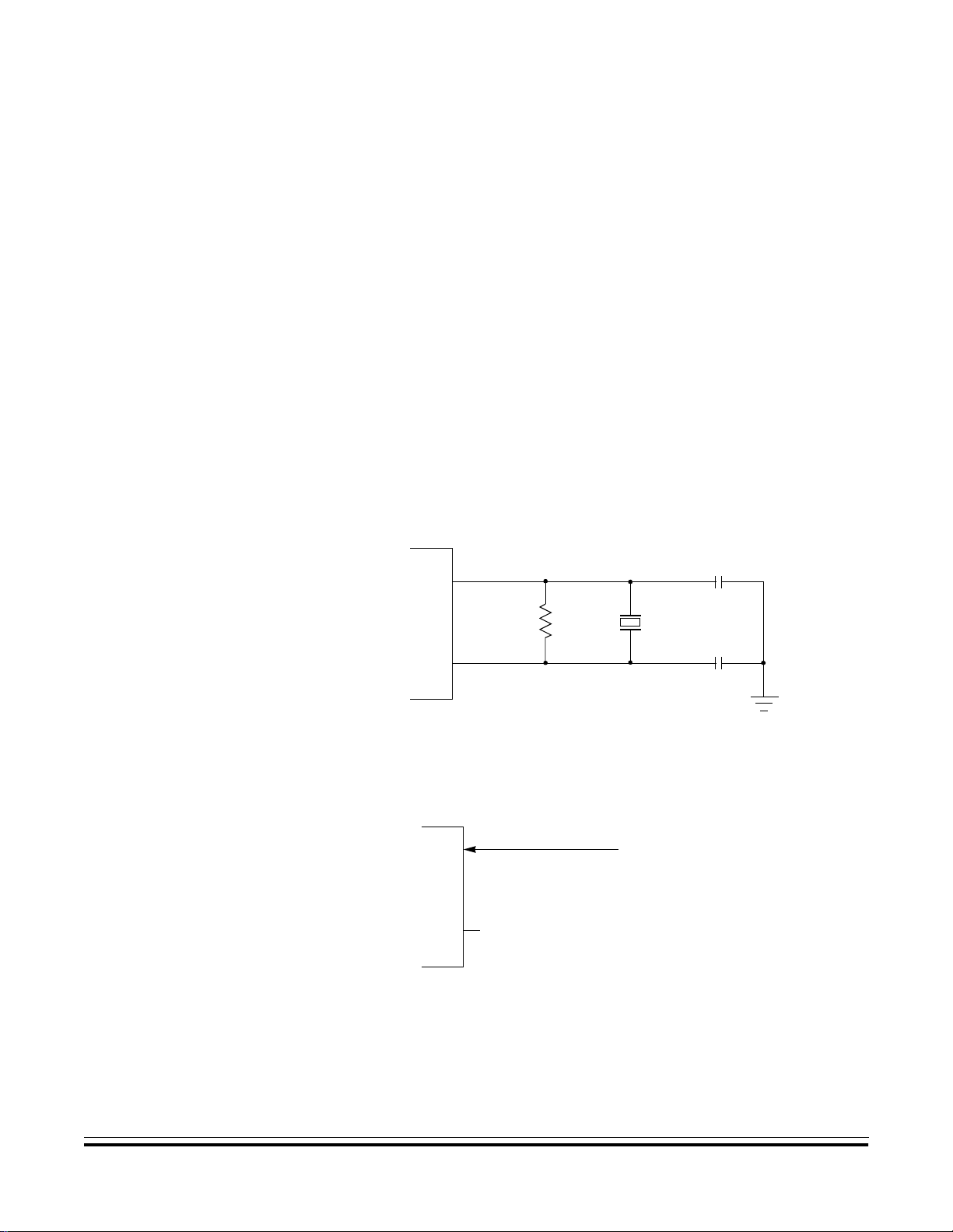
Crystal Driver and External Clock Input (XTAL and EXTAL)
2.5 Crystal Driver and External Clock Input (XTAL and EXTAL)
These two pins provide the interface for either a crystal or a CMOScompatible clock to control the internal clock generator circuitry. The
frequency applied to these pins is four times higher than the desired
E-clock rate.
The XTAL pin must be left unterminated when an external CMOScompatible clock input i s connected to the EXTAL pin. T he XTAL output
is normally intended to drive only a crystal.
CAUTION: In all cases, use caution around the oscillator pins. Load capacitances
shown in the oscillator circuit are specified by the crystal manufacturer
and should include all stray layout capacitances.
Refer to Figure 2-8 and Figure 2-9.
Pin Descriptions
C
L
C
L
MCU
EXTAL
XTAL
10 MΩ
4 x E
CRYSTAL
Figure 2-8. Common Parallel Resonant
Crystal Connections
4 x E
CMOS-COMPATIBLE
MCU
EXTAL
XTAL
EXTERNAL OSCILLATOR
NC
Figure 2-9. External Oscillator Connections
MC68HC11E Family — Rev. 4 Technical Data
MOTOROLA Pin Descriptions 35

Pin Des cr ip t io ns
2.6 E-Clock Output (E)
E is the o utput connection for the internally gen erated E clock. T he signal
from E is used as a ti ming reference. The fr equency of the E-clock out put
is one fourth that of the input frequency at the XTAL and EXTAL pins.
When E-clock outpu t is low , an intern al pr ocess is taking place. When it
is high, data is being accessed.
All clocks, including the E clock, are halted when the MCU is in stop
mode. To reduce R FI emissions, the E-clock output of most E-series
devices can be disabled while operating in single-chip modes.
The E-clock signal is always enabled on the MC68HC811E2.
2.7 Interrupt Request (IRQ)
The IRQ input provides a means of applying asynchronous interrupt
requests to the MCU. Either negative edge-sensitive triggering or
level-sensitive triggering is program selectable (OPTION register). IRQ
is always configured to level-sensitive triggering at reset. When using
IRQ in a level-sensitive wired-OR configuration, connect an external
pullup resistor, typically 4.7 kΩ, to VDD.
2.8 Non-Maskable Interrupt (XIRQ/V
The XIRQ input provides a means of requesting a non-maskable
interrupt after reset initialization. During reset, the X bit in the condition
code register (CCR) is set and any interrupt is masked until MCU
software enable s it. Becau s e the XIR Q input is level- sensitiv e, it can b e
connected to a multiple -source wired-OR network with an external pullup
resistor to VDD. XIRQ is often used as a power loss detect interrupt.
Whenever XIRQ or IRQ is used with multiple interrupt sources each
source must drive the interr upt input with an open -drain type of dri ver to
avoid contention between outputs.
PPE
)
NOTE: IRQ must be configured for level -sensitive operation if the re is more than
one source of IRQ interrupt.
Technical Data MC68HC11E Family — Rev. 4
36 Pin Descriptions MOTOROLA

Pin Descriptions
MODA and MODB (MODA/LIR and MODB/VSTBY)
There should be a single pullup resistor near the MCU interrupt input pin
(typically 4.7 kΩ). There must also be an interlock mechanism at each
interrupt source so that the source holds the interrupt line low until the
MCU recognizes and acknowledg es the interrupt request. If one or more
interrupt sources are still p ending aft er the MCU se rvices a r equest , the
interrupt line will still be held low and the MCU will be interrupted again
as soon as the interrupt mask bit in the MCU is cleared (normally upon
return from an interrupt). Refer to Section 5. Resets and Interrupts.
V
is the input for the 12-volt nominal programming voltage required
PPE
for EPROM/OTPROM programming. On devices without
EPROM/OTPROM, this pin is only an XIRQ
input.
2.9 MODA and MODB (MODA/LIR and MODB/V
During reset, MODA and MODB select one of the four oper ating modes:
• Single-chip mode
• Expanded mode
• Test m ode
• Bootstrap mode
Refer to Section 4. Operating Modes and On-Chip Memory.
After the ope rating mode h as been sel ected, the load instruction regi ster
(LIR) pin provides an open-drain output to indicate that execution of an
instruction has begun. A series of E-clock cycles occurs during
execution of each instruction. The LIR signal goes low during the first
E-clock cycle of each instr uction (opcode fe tch). This outp ut is provide d
for assistance in program debugging.
The V
power. When the voltage on this pin is more than one MOS threshold
(about 0.7 volts) above th e VDD voltage, the internal R AM and part o f the
reset logic are powered from this signal rather than the VDD input. This
allows RAM contents to be retained without VDD power applied to the
MCU. Reset must be driven lo w before VDD is removed and must remain
low until VDD has been restored to a valid level.
pin is used to input random-access memory (R AM) standb y
STBY
STBY
)
MC68HC11E Family — Rev. 4 Technical Data
MOTOROLA Pin Descriptions 37

Pin Des cr ip t io ns
2.10 V
and VRH
RL
2.11 STRA/AS
These two inputs pro vide the reference volta ges for the analog-to- digital
(A/D) converter ci rcuitry:
• VRL is the low reference, typically 0 Vdc.
• VRH is the high reference.
For proper A/D converter operation:
• VRH should be at least 3 Vdc greater than VRL.
• VRL and VRH should be between VSS and VDD.
The strobe A (ST RA) and addre ss strobe (AS) pin p erforms eit her of two
separate functions, depending on the operating mode:
• In single-chip mode, STRA performs an input handshake (strobe
input) function.
2.12 STRB/R/W
• In the expanded multiplexed mode, AS provides an address
strobe function.
AS can be used to demultiplex the address and data signals at port C.
Refer to Section 4. Operating Modes and On-Chip Memory.
The strobe B (STRB) and read/write (R/W) pin act as either an output
strobe or as a data bus direction indicator, depending on the operating
mode.
In single-chip operating mode, STRB acts as a programmab le strobe for
handshake with other parallel devices. Refer to Section 6. Parallel
Input/Output (I/O) Ports for further information.
In expanded multiplexed operating mode, R/W is used to indicate the
direction of transfers on the external data bus. A low on the R/W pin
indicates data is bei ng written to the externa l data bus. A high on this pin
Technical Data MC68HC11E Family — Rev. 4
38 Pin Descriptions MOTOROLA

2.13 Port Signals
Pin Descriptions
Port Signals
indicates that a read cycle is in progress. R/W stays low during
consecutive data bus write cycles, such as a double-byte store. It is
possible for data to be driven out o f port C, if inte rnal r ead visibility (IRV)
is enabled and an internal address is read, even though R/W is in a
high-impedance state. Refer to Section 4. Operating Modes and
On-Chip Memory for more information about IRVNE (internal read
visibility not E).
Port pins have different functions in different operating modes. Pin
functions for port A, port D, and port E are independent of operating
modes. Port B and port C, however, are affected by operating mode.
Port B provides eight general-purpose output signals in single-chip
operating modes. When the microcontroller is in expanded multiplexed
operating mode, port B pins are the eight high-order address lines.
2.13.1 Port A
Port C provides eight general-purpose input/output signals when the
MCU is in t he single-chip operating mod e. When the microcontroll er is in
the expanded multiplexed ope rating mode, por t C pins are a multi plexed
address/data bus.
Refer to Table 2-1 for a functional description of the 40 port signals
within different operating modes. Terminate unused inputs and
input/output (I/O) pins configured as inputs high or low.
In all operating modes, port A can be configured for three timer input
capture (IC) functions a nd four timer outp ut compar e (OC) f unctions. An
additional pin can be configured as either the fourth IC or the fifth OC.
Any port A pin tha t is not curr ently bei ng use d for a timer function can be
used as either a general-purpose input or output line. Only port A pins
PA7 and PA3 have an associated data direction control bit that allows
the pin to be selectively configured as input or output. Bits DDRA7 and
DDRA3 located in PACTL register control data direction for PA7 and
PA3, respective ly. All other port A pins are fixed as either input o r output.
MC68HC11E Family — Rev. 4 Technical Data
MOTOROLA Pin Descriptions 39
Pin Des cr ip t io ns
Table 2-1. Port Sig na l Functions
Port/Bit
PA0 PA0/IC3
PA1 PA1/IC2
PA2 PA2/IC1
PA3 PA3/OC5/IC4/OC1
PA4 PA4/OC4/OC1
PA5 PA5/OC3/OC1
PA6 PA6/OC2/OC1
PA7 PA7/PAI/OC1
PB0 PB0 ADDR8
PB1 PB1 ADDR9
PB2 PB2 ADDR10
PB3 PB3 ADDR11
PB4 PB4 ADDR12
PB5 PB5 ADDR13
PB6 PB6 ADDR14
PB7 PB7 ADDR15
PC0 PC0 ADDR0/DATA0
PC1 PC1 ADDR1/DATA1
PC2 PC2 ADDR2/DATA2
PC3 PC3 ADDR3/DATA3
PC4 PC4 ADDR4/DATA4
PC5 PC5 ADDR5/DATA5
PC6 PC6 ADDR6/DATA6
PC7 PC7 ADDR7/DATA7
PD0 PD0/RxD
PD1 PD1/TxD
PD2 PD2/MISO
PD3 PD3/MOSI
PD4 PD4/SCK
PD5 PD5/SS
— STRA AS
— STRB R/W
PE0 PE0/AN0
PE1 PE1/AN1
PE2 PE3/AN2
PE3 PE3/AN3
PE4 PE4/AN4
PE5 PE5/AN5
PE6 PE6/AN6
PE7 PE7/AN7
Singl e-Chip and
Boots t rap Modes
Expanded and
Test Modes
Technical Data MC68HC11E Family — Rev. 4
40 Pin Descriptions MOTOROLA

Pin Descriptions
Port Signals
PA7 can function as genera l-purpose I /O or as tim er output compare fo r
OC1. PA7 is also the input to the pulse accumulator, even while
functioning as a general-purpose I/O or an OC1 output.
PA6–PA4 serve as either general-p urpose outputs, timer input captu res,
or timer output comp are 2–4. In a ddition, PA6–PA4 can be controlled by
OC1.
PA3 can be a general-purpose I/O pin or a timer IC/OC pin. Timer
functions associated with this pin incl ude OC1 and IC4/OC5. I C4/OC5 is
software selectable as either a fourth input capture or a fifth output
compare. PA3 can al so be configu red to allow OC1 edges to trigger IC 4
captures.
PA2–PA0 serve as general-purpose inputs or as IC1–IC3.
PORTA can be read at any time. Reads of pins configured as inputs
return the logic level present on the pin. Pins configured as outputs
return the logic level present at the pin driver input. If written, PORTA
stores the data in an inter nal latch, bits 7 and 3. I t drives the pin s only if
they are confi gur ed a s out puts. Wri tes to POR TA d o no t chan ge the p i n
state when pins are configured for timer input captures or output
compares. Refer to Section 6. Parallel Input/Output (I/O) Ports.
2.13.2 Port B
During single -chip operat ing modes, al l port B pins are gen eral-purp ose
output pins. During MCU reads of this port, the level sensed at the input
side of the port B ou tput drivers is read. Por t B can also be used in simple
strobed output mode. In thi s mode, an output pulse appear s at the STRB
signal each time data is written to port B.
In expanded multiplexed operating modes, all of the port B pins act as
high order ad dress outp ut sign als. Du ring each MCU cycle, b its 15–8 of
the address bus are output on the PB7–PB0 pins. The PORTB register
is treated as an external address in expanded modes.
MC68HC11E Family — Rev. 4 Technical Data
MOTOROLA Pin Descriptions 41

Pin Des cr ip t io ns
2.13.3 Port C
While in single-chip operating modes, all port C pins are
general-pur pose I/O pins. Port C inputs can be latched into an alternate
PORTCL register by providing an input transition to the STRA signal.
Port C can also be used in full handshake modes of parall el I/O where
the STRA input and STRB output act as handshake control lines.
When in exp ande d m ul tiplexe d m odes, a ll por t C pi n s a re config ured as
multiplexed address/data signals. During the address portion of each
MCU cycle, bits 7–0 of the address are output on the PC7–PC0 pins.
During the data portion of each MCU cycle (E high), PC7–PC0 are
bidirectional data signals, DATA7–DATA0. The direction of data at the
port C pins is indicated by the R/W
signal.
The CWOM con trol bit in the PIOC register disables th e port C P-channel
output driver. CWOM simultaneously affects all eight bits of port C.
Because the N-channel driver is not aff ected by CWOM , setting CWOM
causes port C to become an open-drain type output port suitable for
wired-OR operation.
In wired-OR mode:
• When a port C bit is at logic level 0, it is driven low by the
N-channel driver .
• When a port C bit is at logic level 1, the associated pin has
high-impedance, as neither the N-channel nor the P-channel
devices are active.
It is customary to have an exter nal pullup resistor on lines tha t are driven
by open-drain devices. Port C can only be configured for wired-OR
operation when the MCU is in single-chip mode. Refer to Section 6.
Parallel Input/Ou tput (I/O) Ports for addi tional information about port C
functions.
Technical Data MC68HC11E Family — Rev. 4
42 Pin Descriptions MOTOROLA

2.13.4 Port D
Pin Descriptions
Port Signals
Pins PD5–PD0 can be used for general-pur pose I/O signals. Th ese pins
alternately serve as the seri al com munica tion i nterf ace (SC I) and ser ial
peripheral interfac e (SPI) signals when those subsystems are enabled .
• PD0 is the recei ve data input (RxD) signal for the SCI.
• PD1 is the transmit data output (TxD) signal for the SCI.
• PD5–PD2 are dedicated to the SPI:
– PD2 is the master in/slave out (MISO) signal.
– PD3 is the master out/slave in (MOSI) signal.
– PD4 is the serial clock (SCK) signal.
2.13.5 Port E
CAUTION: If high accuracy is required for A/D conversions, avoid reading port E
– PD5 is the slave select (SS
) input.
Use port E for general-purpose or analog-to-digital (A/D) inputs.
during sampling, as small disturbances can red uce th e accur acy of t hat
result.
MC68HC11E Family — Rev. 4 Technical Data
MOTOROLA Pin Descriptions 43

Pin Des cr ip t io ns
Technical Data MC68HC11E Family — Rev. 4
44 Pin Descriptions MOTOROLA

Technical Data — M68HC11E Family
Section 3. Central Processor Unit (CPU)
3.1 Contents
3.2 Introduction. . . . . . . . . . . . . . . . . . . . . . . . . . . . . . . . . . . . . . . .46
3.3 CPU Registers . . . . . . . . . . . . . . . . . . . . . . . . . . . . . . . . . . . . .46
3.3.1 Accumulators A, B, and D . . . . . . . . . . . . . . . . . . . . . . . . . .4 7
3.3.2 Index Register X (IX) . . . . . . . . . . . . . . . . . . . . . . . . . . . . . .48
3.3.3 Index Register Y (IY) . . . . . . . . . . . . . . . . . . . . . . . . . . . . . .48
3.3.4 Stack Pointer (SP) . . . . . . . . . . . . . . . . . . . . . . . . . . . . . . . .48
3.3.5 Program Counter (PC) . . . . . . . . . . . . . . . . . . . . . . . . . . . . .50
3.3.6 Condition Code Register (CCR). . . . . . . . . . . . . . . . . . . . . .51
3.3.6.1 Carry/Borrow (C) . . . . . . . . . . . . . . . . . . . . . . . . . . . . . . .51
3.3.6.2 Overflow (V). . . . . . . . . . . . . . . . . . . . . . . . . . . . . . . . . . .51
3.3.6.3 Zero (Z) . . . . . . . . . . . . . . . . . . . . . . . . . . . . . . . . . . . . . .51
3.3.6.4 Negative (N). . . . . . . . . . . . . . . . . . . . . . . . . . . . . . . . . . .52
3.3.6.5 Interrupt Mask (I) . . . . . . . . . . . . . . . . . . . . . . . . . . . . . . .52
3.3.6.6 Half Carry (H). . . . . . . . . . . . . . . . . . . . . . . . . . . . . . . . . .52
3.3.6.7 X Interrupt Mask (X). . . . . . . . . . . . . . . . . . . . . . . . . . . . .52
3.3.6.8 STOP Disable (S) . . . . . . . . . . . . . . . . . . . . . . . . . . . . . .53
3.4 Data Types. . . . . . . . . . . . . . . . . . . . . . . . . . . . . . . . . . . . . . . .53
3.5 Opcodes and Operands . . . . . . . . . . . . . . . . . . . . . . . . . . . . . .5 3
3.6 Addressing Modes . . . . . . . . . . . . . . . . . . . . . . . . . . . . . . . . . . 5 4
3.6.1 Immediate. . . . . . . . . . . . . . . . . . . . . . . . . . . . . . . . . . . . . . .54
3.6.2 Direct . . . . . . . . . . . . . . . . . . . . . . . . . . . . . . . . . . . . . . . . . .55
3.6.3 Extended . . . . . . . . . . . . . . . . . . . . . . . . . . . . . . . . . . . . . . . 5 5
3.6.4 Indexed. . . . . . . . . . . . . . . . . . . . . . . . . . . . . . . . . . . . . . . . .55
3.6.5 Inherent . . . . . . . . . . . . . . . . . . . . . . . . . . . . . . . . . . . . . . . .55
3.6.6 Relative . . . . . . . . . . . . . . . . . . . . . . . . . . . . . . . . . . . . . . . .56
3.7 Instruction Set. . . . . . . . . . . . . . . . . . . . . . . . . . . . . . . . . . . . . .56
MC68HC11E Family — Rev. 4 Technical Data
MOTOROLA Central Processor Unit (CPU) 45

Central Processor Unit (C PU)
3.2 Introduction
This section presents information on M68HC11:
• Central processor unit (CPU) architecture
• Data types
• Addressing modes
• Instruction set
• Special operations such as subroutine calls and interrupts
The CPU is designed to treat all peripheral, input/output (I/O), and
memory loca tions identically as a ddresses in the 64-Kbyte memory map.
This is referred to as memory-mapped I/O. There are no special
instructions for I/O that are separate from those used for memory. This
architecture a lso allows accessing an operand from an external memo ry
location with no execution time penalty.
3.3 CPU Registers
M68HC11 CPU registers are an integral part of the CPU and are not
addressed as if they were memory locations. The seven registers,
discussed in the following paragraphs, are shown in Figure 3-1.
Technical Data MC68HC11E Family — Rev. 4
46 Central Processor Unit (CPU) MOTOROLA

Central Processor Unit (CPU)
CPU Registers
7070
15 0
AB
D
IX
IY
SP
PC
70
8-B I T ACCUMULATORS A & B
OR 16-BIT DOUBLE ACCUMULATOR D
INDEX REGISTER X
INDEX REGISTER Y
STACK POINTER
PROGRAM COUNTER
CONDITION CODES
CVZNIHXS
CARRY/BORROW FROM MSB
OVERFLOW
ZERO
NEGATIVE
I-INTERRUPT MASK
HALF CARRY (FROM BIT 3)
X-INTERRUPT MASK
STOP DISABLE
Figure 3-1. Programming Model
3.3.1 Accumulators A, B, and D
Accumulators A and B are general-purpose 8-bit registers that hold
operands and results of arithmetic calculations or data manipulations.
For some instructions, these two accumulators are treated as a single
double-byte (16-bit) accumulator called accumulator D. Although most
instructions can use accumulators A or B interchangeably, these
exceptions apply:
• The ABX and ABY instructions add the contents of 8-bit
accumulator B to the contents of 16-bit register X or Y, but there
are no equivalent instructions that use A instead of B.
• The TAP and TPA instructions transfer data from accumulator A
to the condition code register or from the condition code register
to accumulator A. However, there are no equivalent instructions
that use B rather than A.
MC68HC11E Family — Rev. 4 Technical Data
MOTOROLA Central Processor Unit (CPU) 47

Central Processor Unit (C PU)
• The decimal adjust accumulato r A (DA A) instruction i s used after
binary-coded de cimal (BCD) arithm etic operations, but there is no
equivalent BCD instruction to adjust accumulator B.
• The add, subtract, and com pare instructio ns associate d with both
A and B (ABA, SBA, and CBA) only operate in one direction,
making it important to plan ahead to ensure that the correct
operand is in the correct accumulator.
3.3.2 Index Register X (IX)
The IX register provides a 16- bit indexing value that can be ad ded to the
8-bit offset pr ovided in an instruct ion to create an effective address. T he
IX register can also be used as a counter or as a temporary storage
register.
3.3.3 Index Register Y (IY)
The 16-bit IY regi ste r pe rfor ms a n inde xed m ode function si milar to th at
of the IX register. However, most instructions using the IY register
require an extra byte of machine code and an extra cycle of execution
time because of the way the opcode map is implemented. Refer to
3.5 Opcodes and Operands for further information.
3.3.4 Stack Pointer (SP)
The M68HC11 CPU has an a utomatic pro gram stack. Thi s stack can be
located anywhere in the address space and can be any size up to the
amount of memory a vailable in the system. Normally, the SP is initialized
by one of the first instructions in an application program. The stack is
configured as a data structure that grows downward from high memory
to low memory. Each time a new byte is pushed onto the stack, the SP
is decremented. Each time a byte is pulled from the stack, the SP is
incremented. At any given time, the SP holds the 16-bit address of the
next free location in the stack. Figure 3-2 is a summary of SP
operations.
Technical Data MC68HC11E Family — Rev. 4
48 Central Processor Unit (CPU) MOTOROLA

Central Processor Unit (CPU)
CPU Registers
JSR, JUMP TO SUBROUTINE
MAIN PROGRAM
PC
$9D = JSR
DIRECT
RTN
dd
NEXT MAIN INSTR.
MAIN PROGRAM
PC
$AD = JSR
INDEXED, X
RTN
ff
NEX T MAIN IN S TR.
MAIN PROGRAM
PC
$18 = PRE
INDEXED, Y
RTN
$AD = JSR
ff
NEXT MAIN INSTR.
MAIN PROGRAM
PC
$BD = PRE
INDEXED, Y
RTN
hh
ll
NEXT MAIN INSTR.
BSR, BRANCH TO SUBRO UTINE
MAIN PROGRAM
PC
$8D = BSR
RTS, RETURN FROM
SUBROUTINE
MAIN PROGRAM
PC
$39 = RTS
70
➩ SP–2
SP–1
SP
STACK
70
➩ SP–2
SP–1
SP
SP
SP+1
➩ SP+2
RTN
H
RTN
L
STACK
70
RTN
H
RTN
L
STACK
RTN
RTN
RTI, RETURN FROM INTERRUPT
STACK
INTERRUP T RO UTINE
PC
$3B = RTI
H
L
70
SP
SP+1
SP+2
SP+3
SP+4
SP+5
SP+6
SP+7
SP+8
➩ SP+9
CCR
ACCB
ACCA
IX
H
IX
IY
H
IY
RTN
RTN
L
L
H
L
SWI, SOFTWARE INTERRUPT
STACK
MAIN PROGRAM
PC
$3F = SWI
WAI, WAIT FOR INTERRUPT
MAIN PROGRAM
PC
$3E = WAI
70
➩ SP–9
SP–8
SP–7
SP–6
SP–5
SP–4
SP–3
SP–2
SP–1
SP
CCR
ACCB
ACCA
IX
H
IX
IY
H
IY
RTN
RTN
L
L
H
L
LEGEND:
RTN = ADDRESS OF NEXT INSTRUCTION IN MAIN PROGRAM TO
BE EXECUTED UPON RETURN FROM SUBROUTINE
= MOST SIGNIFICANT BYTE OF RETURN ADDRESS
RTN
H
= LEAST SIGNIFICANT BYTE OF RETURN ADDRESS
RTN
L
➩ = STACK POINTER POSITION AFTER OPERATION IS COMPLETE
dd = 8-BIT DIRECT ADDRESS ($0000–$00FF) (HIGH BYTE ASSUMED
TO BE $00)
ff = 8-BIT POSITIVE OFFSET $00 (0) TO $FF (255) IS ADDED TO INDEX
hh = HIGH-ORDER BYTE OF 16-BIT EXTENDED ADDRESS
ll = LOW-ORDER BYTE OF 16-BIT EXTENDED ADDRESS
rr= SIGNED RELA TIVE OFFSET $80 (–128) TO $7F (+127) (OFFSET
RELATIVE TO THE ADDRESS FOLL OWING THE MACHINE CODE
OFFSET BYTE)
Figure 3-2. Stacking Operations
When a subroutin e is called by a jump-to-subrouti ne (JSR) or bra nch-tosubroutine (BSR) instr uction, the address of the instruction after the JSR
or BSR is automatically pushed onto the stack, least significant byte first.
When the subroutine is finished, a return-from-subroutine (RTS)
instruction is executed. The RTS pulls the previously stacked return
address from the stack and l oads it into the progra m counter. Executi on
then continues at this recovered return address.
MC68HC11E Family — Rev. 4 Technical Data
MOTOROLA Central Processor Unit (CPU) 49

Central Processor Unit (C PU)
When an interrupt is recognized, the current instruction finishes
normally, the return address (the current value in the program counter)
is pushed onto the stack, all of the CPU registers are pushed onto the
stack, and execution continues at the ad dress specified by the ve ctor for
the interrupt.
At the end of the inte rrup t servi ce routin e, an r etur n-fr om i nte rru pt (RT I)
instruction is executed. The RTI instruction causes the saved registers
to be pulled off the stack in reverse order. Program execution resumes
at the return address.
Certain instructions push and pull the A and B accumulators and the X
and Y index registers and are often used to preserve program context.
For example, pushing accumulator A onto the stack when entering a
subroutine that uses accumulator A and then pulling accumulator A off
the stack just before leaving the subroutine ensur es that the contents of
a register will be the same after returning from the subroutine as it was
before starting the subroutine.
3.3.5 Program Counter (PC)
The program coun ter, a 16-bit register, contai ns the addr ess o f the ne xt
instruction to be e xecuted . A fter rese t, the pr ogra m co unter is ini tia lize d
from one of six p ossible vecto rs, de pending on operating mode and the
cause of reset. See Table 3-1.
Mode POR or RESET Pin Clock Monitor COP Watchdog
Normal $FFFE , F $FFFC, D $FFFA, B
Test or Boo t $BFFE, F $BFFC, D $BFFA, B
Table 3-1. Reset Vector Comparison
Technical Data MC68HC11E Family — Rev. 4
50 Central Processor Unit (CPU) MOTOROLA

3.3.6 Condition Code Register (CCR)
This 8-bit register contains:
• Five condition code indicators (C, V, Z, N, and H),
• Two interrupt masking bits (IRQ and XIRQ)
• A stop disable bit (S)
In the M68HC11 CPU, condition codes are updated automatically by
most instructions. For example, load accumulator A (LDAA) and store
accumulator A (STAA) instructions automatically set or clear the N, Z,
and V conditi on code f lags. P ushe s, pu lls, add B to X ( ABX), add B to Y
(ABY), and transfer/exchange instructions do not affect the condition
codes. Refer to Table 3-2, which shows what condition codes are
affected by a particular instruction.
Central Processor Unit (CPU)
CPU Registers
3.3.6.1 Carry/Borrow (C)
The C bit is set if the arithmetic logic unit (ALU) performs a carry or
borrow dur ing an arithmetic o peration. The C bit also acts as an error flag
for multiply and divide operations. Shift and rotate instructions operate
with and through the carry bit to facilitate multiple-word sh ift ope ration s.
3.3.6.2 Overflow (V)
The overflow bit is set if an operation causes an arithmetic overflow.
Otherwise, the V bit is cleared.
3.3.6.3 Zero (Z)
The Z bit is set i f the result of an arithmetic, logic, or data manipulation
operation is 0. Otherwise, the Z bit is cleared. Compare instructions do
an internal implied subtraction and the condition codes, including Z,
reflect the results of that subtraction. A few operations (INX, DEX, INY,
and DEY) affect the Z bit and no other condition flags. For these
operations, only = and ≠ conditions can be determined.
MC68HC11E Family — Rev. 4 Technical Data
MOTOROLA Central Processor Unit (CPU) 51

Central Processor Unit (C PU)
3.3.6.4 Negative (N)
The N bit is set if the result of an arithmetic, logic, or data manipulation
operation is negat ive (MSB = 1). Otherwise, th e N b it is clea red. A result
is said to be ne gativ e if its mo st si gnifican t bit ( MS B) is a 1. A qu ick way
to test whether the conten ts of a mem ory location has the MSB set is to
load it into an accumulator and then check the status of the N bit.
3.3.6.5 Interrupt Mask (I)
The interr upt reque st (IRQ) ma sk (I bit) is a glo bal mask tha t disable s all
maskable interru pt sources. Whil e the I bit is set, inter rupts can beco me
pending, but the operation of the CPU conti nues uninter rup ted until the
I bit is cleared. A fte r an y rese t, the I bit i s se t by d efault and ca n onl y be
cleared by a software i nstructi on. When a n inter rup t is re cognized , the I
bit is set after the registe rs are sta cked, but b efore the interrupt vector is
fetched. After the interrupt has been serviced, a return-from-interrupt
instruction is norma lly executed, restoring the r egisters to the values that
were present before the interrupt occurred. Normally, the I bit is 0 after
a return from interrupt is executed. Although the I bit can be cleared
within an interrupt ser vice routine, " nesting " interr upts in th is way should
only be done when there is a clear understanding of latency and of the
arbitration mechanism. Refer to Section 5. Resets and Interrupts.
3.3.6.6 Half Carry (H)
The H bit is set when a carry occurs between bits 3 and 4 of the
arithmetic l ogic unit during an ADD, ABA, or ADC instru ction. Other wise,
the H bit is cleared. Half carry is used during BCD operations.
3.3.6.7 X Interrupt Mask (X)
The XIRQ mask (X) bit disables interrupts from the XIRQ
pin. After any
reset, X is set by default and must be cleared by a software instruction.
When an XIRQ interrupt is recognized, the X and I bits are set after the
registers are stacked, but befor e the interrupt vector is fetched. A fter the
interrupt has been serviced, an RTI instruction is normally executed,
causing the registers to be restored to the values that were present
before the interrupt occurred. The X interrupt mask bit is set only by
Technical Data MC68HC11E Family — Rev. 4
52 Central Processor Unit (CPU) MOTOROLA

hardware (R ESET or XIR Q a cknowledge). X is clear ed only by pr ogram
instruction (TAP, where the associated bit of A is 0; or RTI, where bit 6
of the value loaded into the CCR from the stack has been clea red) .
There is no hardware action for clearing X.
3.3.6.8 STOP Disable (S)
Setting the STOP disable (S) bit prevents the STOP instruction from
putting the M68HC11 into a low-power stop condition. If the STOP
instruction is encountered by the CPU while the S bit is set, it is treated
as a no-operation (NOP) instruction, and processing continues to the
next instruction. S is set by reset; STOP is disabled by default.
3.4 Data Types
Central Processor Unit (CPU)
Data Types
The M68HC11 CPU supports four data types:
1. Bit data
2. 8-bit and 16-bit signed and unsigned integers
3. 16-bit unsigned fractions
4. 16-bit addresses
A byte is eight bits wide and can be accessed at any byte location. A
word is composed of two consecutive bytes with the most significant
byte at the lower value address. Because the M68HC 11 is an 8-bit CPU ,
there are no special requirements for alignment of instructions or
operands.
3.5 Opcodes and Operands
The M68HC11 Family of microcontrollers uses 8-bit opcodes. Each
opcode identifies a particular instruction and associated addressing
mode to the CPU. Several opcodes are required to provide each
instruction with a range of addressing capabilities. Only 256 opcodes
would be available if the range of values were restricted to the number
able to be expressed in 8-bit binary numbers.
MC68HC11E Family — Rev. 4 Technical Data
MOTOROLA Central Processor Unit (CPU) 53

Central Processor Unit (C PU)
A 4-page opcode map has been implemented to expand the number of
instructions. An additional byte, called a prebyte, directs the processor
from page 0 of the opcode map to one of the other three pages. As its
name implies, the additional byte precedes the opcode.
A complete instruct ion consists of a prebyte, if any, an opcode, and zero,
one, two, or three o perands. The ope rands conta in info rmation th e CPU
needs for executing the instruction. Complete instructions can be from
one to five bytes long.
3.6 Addressing Modes
Six addressing modes can be used to access memory:
• Immediate
• Direct
3.6.1 Immediate
• Extended
• Indexed
• Inherent
• Relative
These modes ar e detailed in the following paragraphs. All modes excep t
inherent mode use an effective address. The effective address is the
memory address from which the argument is fetched or stored or the
address from which execution is to proceed. The effective address can
be specified within an instruction, or it can be calculated.
In the immediate addressing mode, an argument is contained in the
byte(s) immediate ly following the opcode. The numbe r of bytes following
the opcode matches the size of the register or memory location being
operated on. There are 2-, 3-, and 4- (if prebyte is required) byte
immediate instr uctions. Th e eff ecti ve a ddre ss is th e address of the byte
following the instruction.
Technical Data MC68HC11E Family — Rev. 4
54 Central Processor Unit (CPU) MOTOROLA

3.6.2 Direct
3.6.3 Extended
Central Processor Unit (CPU)
Addressing Modes
In the direct addressing mode, the low-order byte of the operand
address is contained in a single byte following the opcode, and the
high-order byte of the address is assumed to be $00. Addresses
$00–$FF are thus accessed directly, using 2-byte instructions.
Execution time is reduced by elim inating the ad diti onal mem ory acces s
required for the high-order address byte. In most applications, this
256-byte area is reserved for frequently referenced data. In M68HC11
MCUs, the memory map can be configu red for combinat io ns of interna l
registers, RAM, or external memory to occupy these addresses.
In the extende d addressing mode , the effective address of the argume nt
is contained in two bytes following the opcode byte. These are 3-byte
instructions (or 4-byte instructions if a prebyte is required). One or two
bytes are needed for the opcode and two for the effective address.
3.6.4 Indexed
3.6.5 Inherent
In the indexed addressing mode, an 8-bit unsigned offset contained in
the instruction is added to the value cont ained in an index reg ister (IX o r
IY). The sum is the effective address. This addressing mode allows
referencing an y memory loca tion in the 64- Kbyte add ress space. Th ese
are 2- to 5-byte instructions, depending on whether or not a prebyte is
required.
In the inherent addressing mode, all the information necessary to
execute the instruction is contained in the opcode. Operations that use
only the index registers or accumulators, as well as control instructions
with no arguments, are included in this addressing mode. These are
1- or 2-byte instructions.
MC68HC11E Family — Rev. 4 Technical Data
MOTOROLA Central Processor Unit (CPU) 55

Central Processor Unit (C PU)
3.6.6 Relative
The relative addre ssing mode is use d only for branch instru ctions. If the
branch condition is true, an 8-bit signed offset included in the instru ction
is added to the contents of the program counter to form the effective
branch address. Otherwise, control proceeds to the next instruction.
These are usually 2-byte instructions.
3.7 Instruction Set
Refer to Table 3-2, which shows all the M68HC11 instructions in all
possible addressing modes. For each instruction, the table shows the
operand constructi on, the number of ma chine code bytes, and execution
time in CPU E-clock cycles.
Technical Data MC68HC11E Family — Rev. 4
56 Central Processor Unit (CPU) MOTOROLA

Central Processor Unit (CPU)
C
0
b7 b0
C
0
b7 b0
C
0
b7 b0
C
0
b7 b0ABb7
b0
C
b7 b0
C
b7 b0
C
b7 b0
Instructi on Set
Table 3-2. Instruction Set (Sheet 1 of 7)
Mnemonic Operation Description
ABA Add
Accumulators
A + B ⇒ AINH1B— 2 —— ∆ — ∆∆∆∆
ABX Add B to X IX + (00 : B) ⇒ IX INH 3A — 3 ————————
ABY Add B to Y IY + (00 : B) ⇒ IY INH 18 3A — 4 ————————
ADCA (opr) Add with Carry
ADCB (opr) Add with Carry
ADDA (opr) Add Memory to
ADDB (opr) Add Memory to
to A
to B
A
B
A + M + C ⇒ A A IMM
B + M + C ⇒ B B IMM
A + M ⇒ A A IMM
B + M ⇒ BBIMM
ADDD (opr) Add 16-Bit to D D + (M : M + 1) ⇒ DIMM
ANDA (opr) AND A with
ANDB (opr) AND B with
Memory
Memory
A • M ⇒ A A IMM
B • M ⇒ B B IMM
ASL (opr) Arithmetic Shift
Left
ASLA Arithmetic Shift
Left A
Addressing Instruction Condition Codes
Mode Opcode Operand Cycles S X H I N Z V C
ADIR
AEXT
A IND,X
A IND,Y
BDIR
BEXT
B IND,X
B IND,Y
ADIR
AEXT
A IND,X
A IND,Y
BDIR
BEXT
B IND,X
B IND,Y
DIR
EXT
IND,X
IND,Y
A DIR
A EXT
A IND,X
A IND,Y
BDIR
BEXT
B IND,X
B IND,Y
EXT
IND,X
IND,Y
99
B9
A9
18 A9
C9
D9
F9
E9
18 E9
8B
9B
BB
AB
18 AB
CB
DB
FB
EB
18 EB
C3
D3
F3
E3
18 E3
84
94
B4
A4
18 A4
C4
D4
F4
E4
18 E4
78
68
18 68
ii
dd
hh ll
ff
ff
ii
dd
hh ll
ff
ff
ii
dd
hh ll
ff
ff
ii
dd
hh ll
ff
ff
jj kk
dd
hh ll
ff
ff
ii
dd
hh ll
ff
ff
ii
dd
hh ll
ff
ff
hh ll
ff
ff
2
——∆ — ∆∆∆∆
3
4
4
5
2
——∆ — ∆∆∆∆
3
4
4
5
2
——∆ — ∆∆∆∆
3
4
4
5
2
——∆ — ∆∆∆∆
3
4
4
5
4
————∆∆∆∆
5
6
6
7
2
————∆∆0 —
3
4
4
5
2
————∆∆0 —
3
4
4
5
6
————∆∆∆∆
6
7
89
AINH 48 — 2 ————∆∆∆∆
ASLB Arithmetic Shift
ASLD Arithmetic Shift
ASR Arithmetic Shift
Left B
Left D
Right
ASRA Arithmetic Shift
BINH 58 — 2 ————∆∆∆∆
INH 05 — 3 ———— ∆∆∆∆
EXT
IND,X
IND,Y
18 67
77
67
hh ll
ff
ff
6
————∆∆∆∆
6
7
AINH 47 — 2 ————∆∆∆∆
Right A
ASRB Arithmetic Shift
BINH 57 — 2 ————∆∆∆∆
Right B
BCC (rel) Branch if Carry
BCLR (opr)
Clear
Clear Bit(s) M • (mm
(msk)
? C = 0 REL 24 rr 3 ————————
) ⇒ M DIR
IND,X
IND,Y
15
1D
18 1D
dd mm
ff mm
ff mm
6
————∆∆0 —
7
8
MC68HC11E Family — Rev. 4 Technical Data
MOTOROLA Central Processor Unit (CPU) 57

Central Processor Unit (C PU)
Table 3-2. Instruction Set (Sheet 2 of 7)
Mnemonic Operation Description
BCS (rel) Branch if Carry
BEQ (rel) Branch if = Zero ? Z = 1 REL 27 rr 3 ————————
BGE (rel) Branch if ∆ Zero ? N ⊕ V = 0 REL 2C rr 3 ————————
BGT (rel) Branch if > Zero ? Z + (N ⊕ V) = 0 REL 2E rr 3 ————————
BHI (rel) Branch if
BHS (rel) Branch if
BITA (opr) Bit(s) Test A
BITB (opr) Bit(s) Test B
BLE (rel) Branch if ∆ Zero ? Z + (N ⊕ V) = 1 REL 2F rr 3 ————————
BLO (rel) Branch if Lower ? C = 1 REL 25 rr 3 ————————
BLS (rel) Branch if Lower
BLT (rel) Branch if < Zero ? N ⊕ V = 1 REL 2D rr 3 ————————
BMI (rel) Branch if Minus ? N = 1 REL 2B rr 3 ————————
BNE (rel) Branch if not =
BPL (rel) Branch if Plus ? N = 0 REL 2A rr 3 ————————
BRA (rel) Branch Always ? 1 = 1 REL 20 rr 3 ————————
BRCLR(opr)
(msk)
(rel)
BRN (rel) Branch Never ? 1 = 0 REL 21 rr 3 ————————
BRSET(opr)
(msk)
(rel)
BSET (opr)
(msk)
BSR (rel) Branch to
BVC (rel) Branch if
BVS (rel) Branch if
CBA Compare A to B A – BINH11— 2 ————∆∆∆∆
CLC Clear Carry Bit 0 ⇒ CINH0C— 2 ——————— 0
CLI Clear Interrupt
CLR (opr) Clear Memory
CLRA Clear
CLRB Clear
CLV Clear O v erflow
CMPA (opr) Compare A to
Set
Higher
Higher or Same
with Memory
with Memory
or Same
Zero
Branch if
Bit(s) Clear
Branch if Bit(s)
Set
Set Bit(s) M + mm ⇒ M DIR
Subroutine
Overflow Clear
Overflow Set
Mask
Byte
Accumulator A
Accumulator B
Flag
Memory
? C = 1 REL 25 rr 3 ————————
? C + Z = 0 REL 22 rr 3 ————————
? C = 0 REL 24 rr 3 ————————
A • M A IMM
B • M B IMM
? C + Z = 1 REL 23 rr 3 ————————
? Z = 0 REL 26 rr 3 ————————
? M • mm = 0 DIR
) • mm = 0 DIR
? (M
See Figure 3–2REL 8Drr 6————————
? V = 0 REL 28 rr 3 ————————
? V = 1 REL 29 rr 3 ————————
0 ⇒ IINH0E— 2 ——— 0 ————
0 ⇒ MEXT
0 ⇒ A A INH 4F — 2 ————0100
0 ⇒ B B INH 5F — 2 ————0100
0 ⇒ VINH0A— 2 —————— 0 —
A – M A IMM
Addressing Instruction Condition Codes
Mode Opcode Operand Cycles S X H I N Z V C
85
ADIR
AEXT
A IND,X
A IND,Y
BDIR
BEXT
B IND,X
B IND,Y
IND,X
IND,Y
IND,X
IND,Y
IND,X
IND,Y
IND,X
IND,Y
ADIR
AEXT
A IND,X
A IND,Y
95
B5
A5
18 A5
C5
D5
F5
E5
18 E5
13
1F
18 1F
12
1E
18 1E
14
1C
18 1C
7F
6F
18 6F
81
91
B1
A1
18 A1
ii
dd
hh ll
ff
ff
ii
dd
hh ll
ff
ff
dd mm rr
ff mm rr
ff mm rr
dd mm rr
ff mm rr
ff mm rr
dd mm
ff mm
ff mm
hh ll
ff
ff
ii
dd
hh ll
ff
ff
2
————∆∆0 —
3
4
4
5
2
————∆∆0 —
3
4
4
5
6
————————
7
8
6
————————
7
8
6
————∆∆0 —
7
8
6
————0100
6
7
2
————∆∆∆∆
3
4
4
5
Technical Data MC68HC11E Family — Rev. 4
58 Central Processor Unit (CPU) MOTOROLA

Central Processor Unit (CPU)
Instructi on Set
Table 3-2. Instruction Set (Sheet 3 of 7)
Mnemonic Operation Description
CMPB (opr) Compare B to
COM (opr) Ones
COMA Ones
COMB Ones
CPD (opr) Compare D to
CPX (opr) Compare X to
CPY (opr) Compare Y to
DAA Decimal Adjust AAdjust Sum to BCD INH 19 — 2 ————∆∆∆∆
Memory
Complement
Memory Byte
Complement
A
Complement
B
Memory 16-Bit
Memory 16-Bit
Memory 16-Bit
B – M B IMM
$FF – M ⇒ MEXT
$FF – A ⇒ A A INH 43 — 2 ————∆∆01
$FF – B ⇒ B B INH 53 — 2 ————∆∆01
D – M : M + 1 IMM
IX – M : M + 1 IMM
IY – M : M + 1 IMM
Addressing Instruction Condition Codes
Mode Opcode Operand Cycles S X H I N Z V C
BDIR
BEXT
B IND,X
B IND,Y
IND,X
IND,Y
DIR
EXT
IND,X
IND,Y
DIR
EXT
IND,X
IND,Y
DIR
EXT
IND,X
IND,Y
C1
D1
F1
E1
18 E1
73
63
18 63
1A 83
1A 93
1A B3
1A A3
CD A3
8C
9C
BC
AC
CD AC
18 8C
18 9C
18 BC
1A AC
18 AC
ii
dd
hh ll
ff
ff
hh ll
ff
ff
jj kk
dd
hh ll
ff
ff
jj kk
dd
hh ll
ff
ff
jj kk
dd
hh ll
ff
ff
2
————∆∆∆∆
3
4
4
5
6
————∆∆01
6
7
5
————∆∆∆∆
6
7
7
7
4
————∆∆∆∆
5
6
6
7
5
————∆∆∆∆
6
7
7
7
DEC (opr) Decrement
DECA Decrement
DECB Decrement
DES Decrement
DEX Decrement
DEY Decrement
EORA (opr) Exclusive OR A
EORB (opr) Exclusive OR B
FDIV Fractional
IDIV Integer Divide
INC (opr) Increment
INCA Increment
Memory Byte
Accumulator
A
Accumulator
B
Stack Pointer
Index Register
X
Index Register
Y
with Memory
with Memory
Divide 16 by 16
16 by 16
Memory Byte
Accumulator
A
M – 1 ⇒ MEXT
A – 1 ⇒ A A INH 4A — 2 ————∆∆∆—
B – 1 ⇒ B B INH 5A — 2 ————∆∆∆—
SP – 1 ⇒ SP INH 34 — 3 ————————
IX – 1 ⇒ IX INH 09 — 3 ————— ∆ ——
IY – 1 ⇒ IY INH 18 09 — 4 ————— ∆ ——
A ⊕ M ⇒ A A IMM
B ⊕ M ⇒ B B IMM
D / IX ⇒ IX; r ⇒ DINH 03— 41 ————— ∆∆∆
D / IX ⇒ IX; r ⇒ DINH 02— 41 ————— ∆ 0 ∆
M + 1 ⇒ MEXT
A + 1 ⇒ A A INH 4C — 2 ————∆∆∆—
IND,X
IND,Y
ADIR
AEXT
A IND,X
A IND,Y
BDIR
BEXT
B IND,X
B IND,Y
IND,X
IND,Y
7A
6A
18 6A
88
98
B8
A8
18 A8
C8
D8
F8
E8
18 E8
7C
6C
18 6C
hh ll
ff
ff
ii
dd
hh ll
ff
ff
ii
dd
hh ll
ff
ff
hh ll
ff
ff
6
————∆∆∆—
6
7
2
————∆∆0 —
3
4
4
5
2
————∆∆0 —
3
4
4
5
6
————∆∆∆—
6
7
MC68HC11E Family — Rev. 4 Technical Data
MOTOROLA Central Processor Unit (CPU) 59
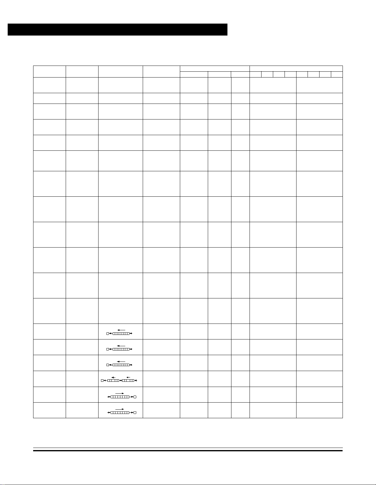
Central Processor Unit (C PU)
C
0
b7 b0
C
0
b7b0C
0
b7 b0
C
0
b7 b0ABb7b0
C
0
b7 b0
C
0
b7 b0
Table 3-2. Instruction Set (Sheet 4 of 7)
Mnemonic Operation Description
INCB Increment
INS Increment
INX Increment
INY Increment
JMP (opr) Jump See Figure 3–2EXT
JSR (opr) Jump to
LDAA (opr) Load
LDAB (opr) Load
LDD (opr) Load Double
LDS (opr) Load Stack
LDX (opr) Load Index
LDY (opr) Load Index
LSL (opr) Logical Shift
LSLA Logical Shift
Accumulator
B
Stack Pointer
Index Register
X
Index Register
Y
Subroutine
Accumulator
A
Accumulator
B
Accumulator
D
Pointer
Register
X
Register
Y
Left
Left A
B + 1 ⇒ B B INH 5C — 2 ————∆∆∆—
SP + 1 ⇒ SP INH 31 — 3 ————————
IX + 1 ⇒ IX INH 08 — 3 —————∆ ——
IY + 1 ⇒ IY INH 18 08 — 4 —————∆ ——
See Figure 3–2DIR
M ⇒ A A IMM
M ⇒ B B IMM
M ⇒ A,M + 1 ⇒ BIMM
M : M + 1 ⇒ SP IMM
M : M + 1 ⇒ IX IMM
M : M + 1 ⇒ IY IMM
Addressing Instruction Condition Codes
Mode Opcode Operand Cycles S X H I N Z V C
IND,X
IND,Y
EXT
IND,X
IND,Y
A DIR
A EXT
A IND,X
A IND,Y
B DIR
B EXT
B IND,X
B IND,Y
DIR
EXT
IND,X
IND,Y
DIR
EXT
IND,X
IND,Y
DIR
EXT
IND,X
IND,Y
DIR
EXT
IND,X
IND,Y
EXT
IND,X
IND,Y
AINH 48 — 2 ————∆∆∆∆
7E
6E
18 6E
9D
BD
AD
18 AD
86
96
B6
A6
18 A6
C6
D6
F6
E6
18 E6
CC
DC
FC
EC
18 EC
8E
9E
BE
AE
18 AE
CE
DE
FE
EE
CD EE
18 CE
18 DE
18 FE
1A EE
18 EE
78
68
18 68
hh ll
ff
ff
dd
hh ll
ff
ff
ii
dd
hh ll
ff
ff
ii
dd
hh ll
ff
ff
jj kk
dd
hh ll
ff
ff
jj kk
dd
hh ll
ff
ff
jj kk
dd
hh ll
ff
ff
jj kk
dd
hh ll
ff
ff
hh ll
ff
ff
3
————————
3
4
5
————————
6
6
7
2
————∆∆0 —
3
4
4
5
2
————∆∆0 —
3
4
4
5
3
————∆∆0 —
4
5
5
6
3
————∆∆0 —
4
5
5
6
3
————∆∆0 —
4
5
5
6
4
————∆∆0 —
5
6
6
6
6
————∆∆∆∆
6
7
LSLB Logical Shift
Left B
LSLD Logical Shift
Left Double
LSR (opr) Logical Shift
Right
LSRA Logical Shift
Right A
BINH 58 — 2 ————∆∆∆∆
INH 05 — 3 ————∆∆∆∆
EXT
IND,X
IND,Y
AINH 44 — 2 ————0 ∆∆∆
18 64
74
64
hh ll
ff
ff
6
————0 ∆∆∆
6
7
Technical Data MC68HC11E Family — Rev. 4
60 Central Processor Unit (CPU) MOTOROLA
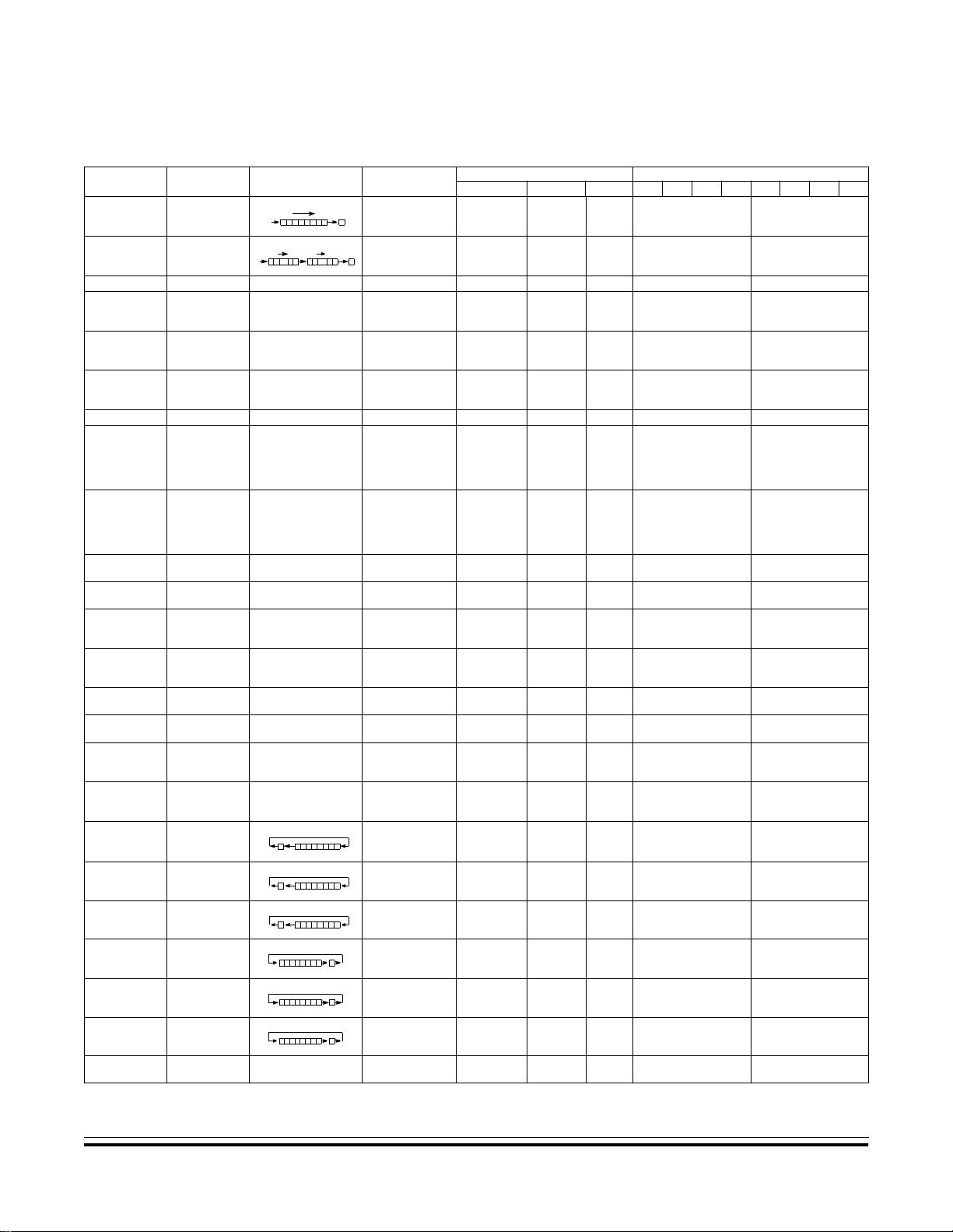
Table 3-2. Instruction Set (Sheet 5 of 7)
C
0
b7 b0
C
0
b7 b0ABb7b0
C
b7 b0
C
b7 b0
C
b7 b0
C
b7 b0
C
b7 b0
C
b7 b0
Mnemonic Operation Description
LSRB Logical Shift
Right B
Central Processor Unit (CPU)
Instructi on Set
Addressing Instruction Condition Codes
Mode Opcode Operand Cycles S X H I N Z V C
BINH 54 — 2 ————0 ∆∆∆
LSRD Logical Shift
Right Double
INH 04 — 3 ———— 0 ∆∆∆
MUL Multiply 8 by 8 A ∗ B ⇒ DINH3D— 10 ——————— ∆
NEG (opr) Two’s
Complement
NEGA Two’s
NEGB Two’s
Memory Byte
Complement
A
Complement
0 – M ⇒ MEXT
IND,X
IND,Y
18 60
70
60
hh ll
ff
ff
6
————∆∆∆∆
6
7
0 – A ⇒ A A INH 40 — 2 ————∆∆∆∆
0 – B ⇒ B B INH 50 — 2 ————∆∆∆∆
B
NOP No operation No Operation INH 01 — 2 ————————
ORAA (opr) OR
ORAB (opr) OR
PSHA Push A onto
Accumulator
A (Inclusive)
Accumulator
B (Inclusive)
Stack
PSHB Push B onto
A + M ⇒ A A IMM
B + M ⇒ B B IMM
ADIR
AEXT
A IND,X
A IND,Y
BDIR
BEXT
B IND,X
B IND,Y
8A
9A
BA
AA
18 AA
CA
DA
FA
EA
18 EA
ii
dd
hh ll
ff
ff
ii
dd
hh ll
ff
ff
2
————∆∆0 —
3
4
4
5
2
————∆∆0 —
3
4
4
5
A ⇒ Stk,SP = SP – 1 A INH 36 — 3 ————————
B ⇒ Stk,SP = SP – 1 B INH 37 — 3 ————————
Stack
PSHX Push X onto
Stack (Lo
PSHY Push Y onto
PULA Pull A from
PULB Pull B from
PULX Pull X Fr om
PULY Pull Y from
First)
Stack (Lo
First)
Stack
Stack
Stack (Hi
First)
Stack (Hi
IX ⇒ Stk,SP = SP – 2 INH 3C — 4 ————————
IY ⇒ Stk,SP = SP – 2 INH 18 3C — 5 ————————
SP = SP + 1, A ⇐ Stk A INH 32 — 4 ————————
SP = SP + 1, B ⇐ Stk B INH 33 — 4 ————————
SP = SP + 2, IX ⇐ Stk INH 38 — 5 ————————
SP = SP + 2, IY ⇐ Stk INH 18 38 — 6 ————————
First)
ROL (opr) Rotate Left EXT
IND,X
IND,Y
18 69
79
69
hh ll
ff
ff
6
————∆∆∆∆
6
7
ROLA Rotate Left A A INH 49 — 2 ————∆∆∆∆
ROLB Rotate Left B B INH 59 — 2 ————∆∆∆∆
ROR (opr) Rotate Right EXT
IND,X
IND,Y
18 66
76
66
hh ll
ff
ff
6
————∆∆∆∆
6
7
RORA Rotate Right A A INH 46 — 2 ————∆∆∆∆
RORB Rotate Right B B INH 56 — 2 ————∆∆∆∆
RTI Return from
Interrupt
See Figure 3–2INH 3B— 12 ∆↓∆∆∆∆∆∆
MC68HC11E Family — Rev. 4 Technical Data
MOTOROLA Central Processor Unit (CPU) 61

Central Processor Unit (C PU)
Table 3-2. Instruction Set (Sheet 6 of 7)
Mnemonic Operation Description
RTS Return from
SBA Subtract B from
SBCA (opr) Subtract with
SBCB (opr) Subtract with
SEC Set Carry 1 ⇒ CINH0D— 2 ——————— 1
SEI Set Interrupt
SEV Set Overflow
STAA (opr) Store
STAB (opr) Store
STD (opr) Store
STOP Stop Internal
STS (opr) Store Stack
STX (opr) Store Index
STY (opr) Store Index
SUBA (opr) Subtract
SUBB (opr) Subtract
SUBD (opr) Subtract
SWI Software
TAB Transfer A to B A ⇒ BINH16— 2 ———— ∆∆0 —
TAP Transfer A to
TBA Transfer B to A B ⇒ AINH17— 2 ———— ∆∆0 —
Subroutine
A
Carry from A
Carry from B
Mask
Flag
Accumulator
A
Accumulator
B
Accumulator
D
Clocks
Pointer
Register X
Register Y
Memory from
A
Memory from
B
Memory from
D
Interrupt
CC Register
See Figure 3–2INH 39— 5 ————————
A – B ⇒ AINH10— 2 ———— ∆∆∆∆
A – M – C ⇒ A A IMM
B – M – C ⇒ B B IMM
1 ⇒ IINH0F— 2 ———1 ————
1 ⇒ VINH0B— 2 ——————1 —
A ⇒ MADIR
B ⇒ MBDIR
A ⇒ M, B ⇒ M + 1 DIR
— INH CF — 2 ————————
SP ⇒ M : M + 1 DIR
IX ⇒ M : M + 1 DIR
IY ⇒ M : M + 1 DIR
A – M ⇒ AAIMM
B – M ⇒ BAIMM
D – M : M + 1 ⇒ DIMM
See Figure 3–2INH 3F— 14 ———1 ————
A ⇒ CCR INH 06 — 2 ∆↓∆∆∆∆∆∆
Addressing Instruction Condition Codes
Mode Opcode Operand Cycles S X H I N Z V C
82
ADIR
AEXT
A IND,X
A IND,Y
BDIR
BEXT
B IND,X
B IND,Y
AEXT
A IND,X
A IND,Y
BEXT
B IND,X
B IND,Y
EXT
IND,X
IND,Y
EXT
IND,X
IND,Y
EXT
IND,X
IND,Y
EXT
IND,X
IND,Y
ADIR
AEXT
A IND,X
A IND,Y
ADIR
AEXT
A IND,X
A IND,Y
DIR
EXT
IND,X
IND,Y
92
B2
A2
18 A2
C2
D2
F2
E2
18 E2
97
B7
A7
18 A7
D7
F7
E7
18 E7
DD
FD
ED
18 ED
9F
BF
AF
18 AF
DF
FF
EF
CD EF
18 DF
18 FF
1A EF
18 EF
80
90
B0
A0
18 A0
C0
D0
F0
E0
18 E0
83
93
B3
A3
18 A3
ii
dd
hh ll
ff
ff
ii
dd
hh ll
ff
ff
dd
hh ll
ff
ff
dd
hh ll
ff
ff
dd
hh ll
ff
ff
dd
hh ll
ff
ff
dd
hh ll
ff
ff
dd
hh ll
ff
ff
ii
dd
hh ll
ff
ff
ii
dd
hh ll
ff
ff
jj kk
dd
hh ll
ff
ff
2
————∆∆∆∆
3
4
4
5
2
————∆∆∆∆
3
4
4
5
3
————∆∆0 —
4
4
5
3
————∆∆0 —
4
4
5
4
————∆∆0 —
5
5
6
4
————∆∆0 —
5
5
6
4
————∆∆0 —
5
5
6
5
————∆∆0 —
6
6
6
2
————∆∆∆∆
3
4
4
5
2
————∆∆∆∆
3
4
4
5
4
————∆∆∆∆
5
6
6
7
Technical Data MC68HC11E Family — Rev. 4
62 Central Processor Unit (CPU) MOTOROLA

Table 3-2. Instruction Set (Sheet 7 of 7)
Mnemonic Operation Description
TEST TEST (Only in
TPA Transfer CC
TST (opr) Test for Ze ro or
TSTA Test A for Zero
TSTB Test B for Zero
TSX Transfer Stack
TSY Transfer Stack
TXS Transfer X to
TYS Transfer Y to
WAI Wait for
XGDX Exchange D
XGDY Exchange D
Test Modes)
Register to A
Minus
or Minus
or Minus
Pointer to X
Pointer to Y
Stack Pointer
Stack Pointer
Interrupt
with X
with Y
Address Bus Counts INH 00 — * ————————
CCR ⇒ AINH07— 2 ————————
M – 0 EXT
A – 0 A INH 4D — 2 ————∆∆00
B – 0 B INH 5D — 2 ————∆∆00
SP + 1 ⇒ IX INH 30 — 3 ————————
SP + 1 ⇒ IY INH 18 30 — 4 ————————
IX – 1 ⇒ SP INH 35 — 3 ————————
IY – 1 ⇒ SP INH 18 35 — 4 ————————
Stack Regs & WAIT INH 3E — ** ————————
IX ⇒ D, D ⇒ IX INH 8F — 3 ————————
IY ⇒ D, D ⇒ IY INH 18 8F — 4 ————————
Central Processor Unit (CPU)
Instructi on Set
Addressing Instruction Condition Codes
Mode Opcode Operand Cycles S X H I N Z V C
7D
IND,X
IND,Y
6D
18 6D
hh ll
ff
ff
6
————∆∆00
6
7
Cycle
* Infinity or until reset occurs
** 12 cycles are used beginning with the opcode fetch. A wait state is entered which remains in effect for an integer number of MPU E-clock
cycles (n) until an interrupt is recognized. Finally, two additional cycles are used to fetch the appropriate interrupt vector (14 + n total).
Operands
dd = 8-bit direct address ($0000–$00FF) (high byte assumed to be $00)
ff = 8-bit positive offset $00 (0) to $FF (255) (is added to index)
hh = High-order byte of 16-bit extended address
ii = One byte of immediate data
jj = High-order byte of 16-bit immediate data
kk = Low-order byte of 16-bit immediate data
ll = Low-order byte of 16-bit extended address
mm = 8-bit mask (set bits to be affected)
rr = Signed relative offset $80 (–128) to $7F (+127)
(offset relative to address following machine code offset byte))
Operators
( ) Contents of register shown inside parentheses
⇐ Is transferred to
⇑ Is pulled from stack
⇓ Is pushed onto stack
• Boolean AND
+ Arithmetic addition symbol except where used as inclusive-OR symbol
in Boolean formula
⊕ Exclusive-OR
∗ Multiply
: Concatenation
– Arithmetic subtraction symbol or negation symbol (two’s complement)
Condition Codes
— Bit not changed
0 Bit always cleared
1Bit always set
∆ Bit cleared or set, depending on operation
↓ Bit can be cleared, cannot become set
MC68HC11E Family — Rev. 4 Technical Data
MOTOROLA Central Processor Unit (CPU) 63

Central Processor Unit (C PU)
Technical Data MC68HC11E Family — Rev. 4
64 Central Processor Unit (CPU) MOTOROLA

Technical Data — M68HC11E Family
Section 4. Operating Modes and On-Chip Memory
4.1 Contents
4.2 Introduction. . . . . . . . . . . . . . . . . . . . . . . . . . . . . . . . . . . . . . . .66
4.3 Operating Modes . . . . . . . . . . . . . . . . . . . . . . . . . . . . . . . . . . .66
4.3.1 Single-Chip Mode. . . . . . . . . . . . . . . . . . . . . . . . . . . . . . . . .66
4.3.2 Expanded Mode. . . . . . . . . . . . . . . . . . . . . . . . . . . . . . . . . .67
4.3.3 Test Mode . . . . . . . . . . . . . . . . . . . . . . . . . . . . . . . . . . . . . .67
4.3.4 Bootstrap Mode . . . . . . . . . . . . . . . . . . . . . . . . . . . . . . . . . .68
4.4 Memory Map. . . . . . . . . . . . . . . . . . . . . . . . . . . . . . . . . . . . . . .6 9
4.4.1 RAM and Input/Output Mapping. . . . . . . . . . . . . . . . . . . . . .80
4.4.2 Mode Selection. . . . . . . . . . . . . . . . . . . . . . . . . . . . . . . . . . .82
4.4.3 System Initialization . . . . . . . . . . . . . . . . . . . . . . . . . . . . . . .85
4.4.3.1 System Configuration Register . . . . . . . . . . . . . . . . . . . .86
4.4.3.2 RAM and I/O Mapping Register . . . . . . . . . . . . . . . . . . . .89
4.4.3.3 System Configuration Options Register. . . . . . . . . . . . . .91
4.5 EPROM/OTPROM . . . . . . . . . . . . . . . . . . . . . . . . . . . . . . . . . .92
4.5.1 Programming an Individual EPROM Address . . . . . . . . . . .93
4.5.2 Programming the EPROM with Downloaded Data. . . . . . . .94
4.5.3 EPROM and EEPROM Programming Control Register. . . .94
4.6 EEPROM . . . . . . . . . . . . . . . . . . . . . . . . . . . . . . . . . . . . . . . . .98
4.6.1 EEPROM and CONFIG Programming and Erasure. . . . . . .98
4.6.1.1 Block Protect Register . . . . . . . . . . . . . . . . . . . . . . . . . . .9 9
4.6.1.2 EPROM and EEPROM Programming
Control Register . . . . . . . . . . . . . . . . . . . . . . . . . . . .101
4.6.1.3 EEPROM Bulk Erase. . . . . . . . . . . . . . . . . . . . . . . . . . .103
4.6.1.4 EEPROM Row Erase. . . . . . . . . . . . . . . . . . . . . . . . . . .103
4.6.1.5 EEPROM Byte Erase. . . . . . . . . . . . . . . . . . . . . . . . . . .104
4.6.1.6 CONFIG Register Programming . . . . . . . . . . . . . . . . . .104
4.6.2 EEPROM Security . . . . . . . . . . . . . . . . . . . . . . . . . . . . . . .104
MC68HC11E Family — Rev. 4 Technical Data
MOTOROLA Operating Modes and On-Chip Memory 65

Operating Modes and On-Chip Memory
4.2 Introduction
This section contains information about the operating modes and the
on-chip memory for M68HC11 E-series MCUs. Except for a few minor
differences, operation is identical for all devices in the E series.
Differences are noted where necessary.
4.3 Operating Modes
The values of the mode select inputs MODB and MODA during reset
determine the operating mode. Single-chip and expanded multiplexed
are the normal modes.
• In single-chip mode only on-chip memory is available.
• Expanded mode, however, allows access to external memory.
Each of the two normal modes is paired with a special mode:
4.3.1 Single-Chip Mode In single-chip mode, ports B and C and strobe pins A (STRA) and B
(STRB) are available for general-purpose parallel input/output (I/O). In
this mode, all software needed to control the MCU is contained in
internal resource s. If present, read-only memory ( ROM) and/or er asable,
programmable read-only memory (EPROM) will always be enabled out
of reset, ensuring that the re set and interrupt vecto rs will be available at
locations $FFC0–$FFFF.
NOTE: For the MC68HC811E2, the vector locations are the same; however,
they are contained in the 2048-byte EEPROM array.
• Bootstrap, a variation of the single-chip mode, is a special mode
that executes a bo otloader progra m in an internal boo tstrap ROM.
• Test is a special mode that allows privileged access to internal
resources.
Technical Data MC68HC11E Family — Rev. 4
66 Operating Modes and On-Chip Memory MOTOROLA

4.3.2 Expanded Mode
Operating Modes and On-Chip Memory
Operating Modes
In expanded operating mode, the MCU can access the full 64-Kbyte
address space. The space includes:
• The same on-chip memory addresses used for single-chip mode
• Addresses for external peripherals and memory devices
The expansion bus is made up of ports B and C, and control signals AS
(address strobe) and R/W (r ead/ wri te). R /W and AS allow the low-order
address and the 8-bit data bus to be multiplexed on the same pins.
During the first half of each bus cycle address information is present.
During the second half of each bus cycle the pins become the
bidirectional data bus. AS is an active-high latch enable signal for an
external address latch. Address information is allowed through the
transparent latch while AS is high and is latched when AS drives low.
NOTE: The write enable signal for an external memory is the NAND of the
4.3.3 Test Mode
The address, R /W
, and AS signals are active and valid for all bus cycles,
including accesses to i nternal memor y l ocatio ns. The E clock is used to
enable external devices to drive data onto the internal data bus during
the second half of a read bus cycle (E clock high). R/W controls the
direction of data tr ansfer s. R/W
drives low when data is being written to
the internal data bus. R/W will remain low during consecutive data bus
write cycles, such as when a double-byte store occurs.
Refer to Figure 4-1.
E clock and the inverted R/W signal.
Test mode, a variation of the expanded mode, is primarily used during
Motorola’s internal production testing; however, it is accessible for
programming the configuration (CONFIG) register, programming
calibration data into electrically erasable, programmable read-only
memory (EEPROM), and supporting emulation and debugging during
development.
MC68HC11E Family — Rev. 4 Technical Data
MOTOROLA Operating Modes and On-Chip Memo ry 67

Operating Modes and On-Chip Memory
PB7
PB6
PB5
PB4
PB3
PB2
PB1
MCU
PB0
PC7
PC6
PC5
PC4
PC3
PC2
PC1
PC0
AS
R/W
E
HC373
D1
D2
D3
D4
D5
D6
D7
D8
LE
Figure 4-1. Address /Data De multip lexin g
Q1
Q2
Q3
Q4
Q5
Q6
Q7
Q8
OE
ADDR15
ADDR14
ADDR13
ADDR12
ADDR11
ADDR10
ADDR9
ADDR8
ADDR7
ADDR6
ADDR5
ADDR4
ADDR3
ADDR2
ADDR1
ADDR0
WE
OE
DATA7
DATA6
DATA5
DATA4
DATA3
DATA2
DATA1
DATA0
4.3.4 Bootstrap Mode
When the MCU is reset in special bootstrap mode, a small on-chip
read-only memory (ROM) is enabled at address $BF00–$BFFF. The
ROM contains a bootloader program and a special set of interrupt and
reset vectors. The MCU fetches the reset vector, then executes the
bootloader.
Bootstrap mode is a specia l variation of the single-chip mode . Bootstrap
mode allows special-purpose programs to be entered into internal
random-access memory (RAM). When bootstrap mode is selected at
reset, a small bootstrap ROM becomes present in the memory map.
Reset and interrupt vectors are located in this ROM at $BFC0–$BFFF.
The bootstrap RO M contai ns a sma ll program which initializ es the seri al
communications interface (SCI) and allows the user to download a
program int o on-chip RA M. The size of the do wnloaded program can be
as large as the si ze of the on-chip RAM. After a 4-character delay, or
after receiving the character for the highest address in RAM, control
Technical Data MC68HC11E Family — Rev. 4
68 Operating Modes and On-Chip Memory MOTOROLA

4.4 Memory Map
Operating Modes and On-Chip Memory
Memory Map
passes to the loaded prog ram at $0000. Refer to Fig ure 4-2, Figure 4-3,
Figure 4-4, Figure 4-5, and Figure 4-6.
Use of an external pullup resistor is required when using the SCI
transmitter pi n because port D pins are configured for wired-OR
operation by th e bootloader. In bootstrap mode, the interru pt vectors are
directed to RAM . This all ows th e use of in terr upts thr ough a jump t able.
Refer to the application note AN1060 entitled M68HC11 Bootstrap
Mode, that is included in this data book.
The operat ing mode determ ines memory ma pping and whe ther external
addresses can be accessed. Refer to Fig ure 4-2, Figure 4-3,
Figure 4-4, Figure 4-5, and Figure 4-6, which illustra te the memory
maps for each of the three families comprising the M68HC11 E series of
MCUs.
Memory locat ions for on-chip resources are the same for both expande d
and single-chip modes. Control bits in the configuration (CONFIG)
register allow EPROM and EEPROM (if pr esent) to be disabled fro m the
memory map . The RAM is map ped to $0000 after reset. It can be p laced
at any 4-Kbyte boundary ($x000) by writing an appropriate value to the
RAM and I/O map re gister ( INIT). The 64-b yte re gister b l ock is map ped
to $1000 after reset and also can be placed at any 4-Kbyte boundary
($x000) by writing an app ropr iate val ue to the INIT reg ister. If R AM and
registers are mapped to the same boundary, the first 64 bytes of RAM
will be inaccessible.
Refer to Figure 4-7, which details the MCU register and control bit
assignments. Reset states shown are for single-chip mode only.
MC68HC11E Family — Rev. 4 Technical Data
MOTOROLA Operating Modes and On-Chip Memo ry 69

Operating Modes and On-Chip Memory
$0000
$1000
$B600
$D000
$FFFF
EXT
EXT EXT
EXPANDED
BOOTSTRAP SPECIAL
Figure 4-2. Me mory Map for MC68 HC11E0
EXT
TEST
0000
512 BYTES RAM
01FF
1000
64-BYTE REGIST ER BLOC K
103F
BOOT
BF00
ROM
BFFF
NORMAL
FFC0
MODES
INTERRUPT
FFFF
VECTORS
BFC0
BFFF
SPECIAL MODES
INTERRUPT
VECTORS
$0000
$1000
$B600
$D000
$FFFF
EXT
EXT EXT
EXT
EXPANDED
BOOTSTRAP SPECIAL
Figure 4-3. Me mory Map for MC68 HC11E1
EXT
EXT
TEST
0000
512 BYTES RAM
01FF
1000
64-BYTE REGISTE R BLO CK
103F
B600
512 BYTES EEPROM
B7FF
BOOT
BF00
ROM
BFFF
NORMAL
FFC0
MODES
INTERRUPT
FFFF
VECTORS
BFC0
BFFF
SPECIAL MODES
INTERRUPT
VECTORS
Technical Data MC68HC11E Family — Rev. 4
70 Operating Modes and On-Chip Memory MOTOROLA

Operating Modes and On-Chip Memory
Memory Map
$0000
$1000
$B600
$D000
$FFFF
SINGLE
CHIP
0000
EXT
EXT EXT
EXT
EXPANDED
BOOTSTRAP SPECIAL
EXT
EXT
TEST
512 BYTES RAM
01FF
1000
64-BYTE REGISTER BLOCK
103F
B600
512 BYTES EEPROM
B7FF
BOOT
BF00
ROM
BFFF
12 KBYTES ROM/EPROM
D000
FFFF
Figure 4-4. Memory Map for MC68HC(7)11E9
BFC0
BFFF
FFC0
FFFF
SPECIAL MODES
INTERRUPT
VECTORS
NORMAL
MODES
INTERRUPT
VECTORS
$0000
EXT
$1000
EXT
$9000
EXT
$B600
EXT
$D000
$FFFF
SINGLE
CHIP
* 20 Kbytes RO M/EPROM are contained in two se gments of 8 Kbytes and 12 Kbytes each.
EXPANDED
BOOTSTRAP SPECIAL
EXT
EXT
EXT
EXT
TEST
0000
768 BYTES RAM
02FF
1000
64-BYTE REGISTER BLOC K
103F
9000
8 KBYTES ROM/EPROM *
AFFF
B600
512 BYTES EEPROM
B7FF
BOOT
BF00
ROM
BFFF
12 KBYTES ROM/EPROM *
D000
FFFF
Figure 4-5. Memory Map for MC68HC(7)11E20
BFC0
BFFF
FFC0
FFFF
SPECIAL MODES
INTERRUPT
VECTORS
NORMAL
MODES
INTERRUPT
VECTORS
MC68HC11E Family — Rev. 4 Technical Data
MOTOROLA Operating Modes and On-Chip Memo ry 71

Operating Modes and On-Chip Memory
$0000
$1000
$F800
$FFFF
SINGLE
CHIP
0000
EXT
EXT EXT
EXPANDED
BOOTSTRAP SPECIAL
EXT
TEST
00FF
1000
103F
BF00
BFFF
F800
FFFF
Figure 4-6. Memory Map for MC68HC811E2
256 BYTES RAM
64-BYTE REGISTER BLOCK
BOOT
ROM
2048 BYTES EEPRO M
BFC0
BFFF
FFC0
FFFF
SPECIAL MODES
INTERRUPT
VECTORS
NORMAL
MODES
INTERRUPT
VECTORS
Addr. Register Name Bit 7 6 5 4 3 2 1 Bit 0
Read:
PA7 PA6 PA5 PA4 PA3 PA2 PA1 PA0
Write:
Reset: I 0 0 0 I I I I
$1000
Port A Data Register
(PORTA)
See page 134.
$1001 Reserved R R R R R R R R
Read:
STAF STAI CWOM HNDS OIN PLS EGA INVB
Write:
Reset: 0 0 0 0 0 U 1 1
$1002
Parallel I/O Control Register
(PIOC)
See page 141.
= Unimplemented R = Reserved U = Unaffected
I = Indeterminate after reset
Figure 4-7. Register and Control Bit Assignments (Sheet 1 of 8)
Technical Data MC68HC11E Family — Rev. 4
72 Operating Modes and On-Chip Memory MOTOROLA

Operating Modes and On-Chip Memory
Memory Map
Addr. Register Name Bit 7 6 5 4 3 2 1 Bit 0
Port C Data Re gister
$1003
Port B Data Register
$1004
Port C Latched Register
$1005
$1006 Reserved R R R R R R R R
Port C Data Direction Regist er
$1007
Port D Data Re gister
$1008
(PORTC)
See page 136.
(PORTB)
See page 136.
(PORTCL)
See page 137.
(DDRC)
See page 137.
(PORTD)
See page 138.
Read:
PC7 PC6 PC5 PC4 PC3 PC2 PC1 PC0
Write:
Reset: Indeterminate after reset
Read:
PB7 PB6 PB5 PB4 PB3 PB2 PB1 PB0
Write:
Reset: 0 0 0 0 0 0 0 0
Read:
PCL7 P C L6 PCL5 PCL4 PC L3 PCL2 PCL1 P C L0
Write:
Reset: Indeterminate after reset
Read:
DDRC7 DDRC6 DDRC5 DDRC4 DDRC3 DDRC2 DDRC1 DDRC0
Write:
Reset: 0 0 0 0 0 0 0 0
Read:
0 0 PD5 PD4 PD3 PD2 PD1 PD0
Write:
Reset: U U I I I I I I
Read:
DDRD5 DDRD4 DDRD3 DDRD2 DDRD1 DDRD0
Write:
Reset: 0 0 0 0 0 0 0 0
Read:
PE7 PE6 PE5 PE4 PE3 PE2 PE1 PE0
Write:
Reset: Indeterminate after reset
Read:
FOC1 FOC2 FOC3 FOC4 FOC5
Write:
Reset: 0 0 0 0 0 0 0 0
= Unimplemented R = Reserved U = Unaffected
I = Indeterminate after reset
$1009
$100A
$100B
Port D Data Direction Regist er
(DDRD)
See page 138.
Port E Data Register
(PORTE)
See page 139.
Timer Compare Force
Register (CFORC)
See page 190.
Figure 4-7. Register and Control Bit Assignments (Sheet 2 of 8)
MC68HC11E Family — Rev. 4 Technical Data
MOTOROLA Operating Modes and On-Chip Memo ry 73

Operating Modes and On-Chip Memory
Addr. Register Name Bit 7 6 5 4 3 2 1 Bit 0
Output Compare 1 Mask
$100C
Output Compare 1 Data
$100D
Timer Counter Register High
$100E
Timer Counter Register Low
$100F
Timer Input Capture 1 Register
$1010
Timer Input Capture 1 Register
$1011
Register (OC1M)
See page 191.
Register (OC1D)
See page 192.
(TCNTH)
See page 193.
(TCNTL)
See page 193.
High (TIC1H)
See page 184.
Low (TIC1L)
See page 184.
Read:
OC1M7 OC1M6 OC1M5 OC1M4 OC1M3
Write:
Reset: 0 0 0 0 0 0 0 0
Read:
OC1D7 OC1D6 O C1D5 OC1D4 OC1D3
Write:
Reset: 0 0 0 0 0 0 0 0
Read: Bit 15 Bit 14 Bit 13 Bit 12 Bit 11 Bit 10 Bit 9 Bit 8
Write:
Reset: 0 0 0 0 0 0 0 0
Read: Bit 7 Bit 6 Bit 5 Bit 4 Bit 3 Bit 2 Bit 1 Bit 0
Write:
Reset: 0 0 0 0 0 0 0 0
Read:
Bit 15 Bit 14 Bit 13 Bit 12 Bit 11 Bit 10 Bit 9 Bit 8
Write:
Reset: Indeterminate after reset
Read:
Bit 7 Bit 6 Bit 5 Bit 4 Bit 3 Bit 2 Bit 1 Bit 0
Write:
Reset: Indeterminate after reset
Timer Input Capture 2 Register
$1012
TImer Input Capture 2
$1013
Timer Input Capture 3 Register
$1014
Register Low (TIC2L)
High (TIC2H)
See page 185.
See page 185.
High (TIC3H)
See page 185.
Read:
Bit 15 Bit 14 Bit 13 Bit 12 Bit 11 Bit 10 Bit 9 Bit 8
Write:
Reset: Indeterminate after reset
Read:
Bit 7 Bit 6 Bit 5 Bit 4 Bit 3 Bit 2 Bit 1 Bit 0
Write:
Reset: Indeterminate after reset
Read:
Bit 15 Bit 14 Bit 13 Bit 12 Bit 11 Bit 10 Bit 9 Bit 8
Write:
Reset: Indeterminate after reset
= Unimplemented R = Reserved U = Unaffected
I = Indeterminate after reset
Figure 4-7. Register and Control Bit Assignments (Sheet 3 of 8)
Technical Data MC68HC11E Family — Rev. 4
74 Operating Modes and On-Chip Memory MOTOROLA

Operating Modes and On-Chip Memory
Memory Map
Addr. Register Name Bit 7 6 5 4 3 2 1 Bit 0
Timer Input Capture 3 Register
$1015
Timer Output Compare 1
$1016
$1017
$1018
$1019
$101A
Register High (TOC1H)
Timer Output Compare 1
Register Low (TOC1L)
Timer Output Compare 2
Register High (TOC2H)
Timer Output Compare 2
Register Low (TOC2L)
Timer Output Compare 3
Register High (TOC3H)
Low (TIC3L)
See page 185.
See page 188.
See page 188.
See page 188.
See page 188.
See page 189.
Read:
Bit 7 Bit 6 Bit 5 Bit 4 Bit 3 Bit 2 Bit 1 Bit 0
Write:
Reset: Indeterminate after reset
Read:
Bit 15 Bit 14 Bit 13 Bit 12 Bit 11 Bit 10 Bit 9 Bit 8
Write:
Reset: 1 1 1 1 1 1 1 1
Read:
Bit 7 Bit 6 Bit 5 Bit 4 Bit 3 Bit 2 Bit 1 Bit 0
Write:
Reset: 1 1 1 1 1 1 1 1
Read:
Bit 15 Bit 14 Bit 13 Bit 12 Bit 11 Bit 10 Bit 9 Bit 8
Write:
Reset: 1 1 1 1 1 1 1 1
Read:
Bit 7 Bit 6 Bit 5 Bit 4 Bit 3 Bit 2 Bit 1 Bit 0
Write:
Reset: 1 1 1 1 1 1 1 1
Read:
Bit 15 Bit 14 Bit 13 Bit 12 Bit 11 Bit 10 Bit 9 Bit 8
Write:
Reset: 1 1 1 1 1 1 1 1
Read:
Bit 7 Bit 6 Bit 5 Bit 4 Bit 3 Bit 2 Bit 1 Bit 0
Write:
Reset: 1 1 1 1 1 1 1 1
Read:
Bit 15 Bit 14 Bit 13 Bit 12 Bit 11 Bit 10 Bit 9 Bit 8
Write:
Reset: 1 1 1 1 1 1 1 1
Read:
Bit 7 Bit 6 Bit 5 Bit 4 Bit 3 Bit 2 Bit 1 Bit 0
Write:
Reset: 1 1 1 1 1 1 1 1
= Unimplemented R = Reserved U = Unaffected
I = Indeterminate after reset
$101B
$101C
$101D
Timer Output Compare 3
Register Low (TOC3L)
See page 189.
Timer Output Compare 4
Register High (TOC4H)
See page 189.
Timer Output Compare 4
Register Low (TOC4L)
See page 189.
Figure 4-7. Register and Control Bit Assignments (Sheet 4 of 8)
MC68HC11E Family — Rev. 4 Technical Data
MOTOROLA Operating Modes and On-Chip Memo ry 75
Operating Modes and On-Chip Memory
Addr. Register Name Bit 7 6 5 4 3 2 1 Bit 0
$101E
$101F
$1020
$1021
$1022
$1023
Timer Input Capture 4/Output
Compare 5 Register High
(TI4/O5) See page 186.
Timer Input Capture 4/Output
Compare 5 Register Low
(TI4/O5) See page 186.
Timer Control Register 1
(TCTL1)
See page 194.
Timer Control Register 2
(TCTL2)
See page 183.
Timer In terrupt Mask 1
Register (TMSK1)
See page 195.
Timer Interrupt Flag 1
(TFLG1)
See page 196.
Read:
Bit 15 Bit 14 Bit 13 Bit 12 Bit 11 Bit 10 Bit 9 Bit 8
Write:
Reset: 1 1 1 1 1 1 1 1
Read:
Bit 7 Bit 6 Bit 5 Bit 4 Bit 3 Bit 2 Bit 1 Bit 0
Write:
Reset: 1 1 1 1 1 1 1 1
Read:
OM2 OL2 OM3 OL3 O M4 OL4 O M5 OL5
Write:
Reset: 0 0 0 0 0 0 0 0
Read:
EDG4B EDG4A EDG1B EDG1A EDG2B EDG2A EDG3B EDG3A
Write:
Reset: 0 0 0 0 0 0 0 0
Read:
OC1I OC2I OC3I OC4I I4/O5I IC1I IC 2I IC3I
Write:
Reset: 0 0 0 0 0 0 0 0
Read:
OC1F OC2F OC3F OC4F I4/O5F IC1F IC2F IC3F
Write:
Reset: 0 0 0 0 0 0 0 0
Read:
TOI RTII PAOVI PAII
Write:
Reset: 0 0 0 0 0 0 0 0
Read:
TOF RTIF PAOVF PAIF
Write:
Reset: 0 0 0 0 0 0 0 0
Read:
DDRA7 PAEN PAMOD PEDGE DDRA3 I4/O5 RTR1 RTR0
Write:
Reset: 0 0 0 0 0 0 0 0
= Unimplemented R = Reserved U = Unaffected
I = Indeterminate after reset
PR1 PR0
$1024
$1025
$1026
Timer In terrupt Mask 2
Register (TMSK2)
See page 196.
Timer Interrupt Flag 2
(TFLG2)
See page 201.
Pulse Accumulator Control
Register (PACTL)
See page 202.
Figure 4-7. Register and Control Bit Assignments (Sheet 5 of 8)
Technical Data MC68HC11E Family — Rev. 4
76 Operating Modes and On-Chip Memory MOTOROLA

Operating Modes and On-Chip Memory
Memory Map
Addr. Register Name Bit 7 6 5 4 3 2 1 Bit 0
$1027
$1028
$1029
$102A
$102B
$102C
Pulse Accumulator Count
Register (PACNT)
See page 206.
Serial Peripheral Control
Register (SPCR)
See page 173.
Serial Peripheral Status
Register (SPSR)
See page 175.
Serial Peripheral Data I/O
Register (SPDR)
See page 176.
Baud Rate Register
(BAUD)
See page 157.
Serial Communications
Control Register 1 (SCCR1)
See page 153.
Read:
Write:
Reset: Indeterminate after reset
Read:
Write:
Reset: 0 0 0 0 0 1 U U
Read:
Write:
Reset: 0 0 0 0 0 0 0 0
Read:
Write:
Reset: Indeterminate after reset
Read:
Write:
Reset: 0 0 0 0 0 U U U
Read:
Write:
Reset: I I 0 0 0 0 0 0
Bit 7 Bit 6 Bit 5 Bit 4 Bit 3 Bit 2 Bit 1 Bit 0
SPIE SPE DWOM MSTR C POL CPHA SPR1 SPR0
SPIF WCOL
Bit 7 Bit 6 Bit 5 Bit 4 Bit 3 Bit 2 Bit 1 Bit 0
TCLR SCP2
R8 T8
(1)
SCP1 SCP0 RCKB SCR2 SCR1 SCR0
MODF
M WAKE
Serial Communications
$102D
$102E
1. SCP2 adds ÷39 to SCI prescaler and is present only in MC68HC(7)11E20.
Control Register 2 (SCCR2)
See page 154.
Serial Communications Status
Register (SCSR)
See page 155.
Read:
TIE TCIE RIE ILIE TE RE RWU SBK
Write:
Reset: 0 0 0 0 0 0 0 0
Read:
TDRE TC RDRF IDLE O R NF FE
Write:
Reset: 1 1 0 0 0 0 0 0
= Unimplemented R = Reserved U = Unaffected
I = Indeterminate after reset
Figure 4-7. Register and Control Bit Assignments (Sheet 6 of 8)
MC68HC11E Family — Rev. 4 Technical Data
MOTOROLA Operating Modes and On-Chip Memo ry 77

Operating Modes and On-Chip Memory
Addr. Register Name Bit 7 6 5 4 3 2 1 Bit 0
$102F
$1030
$1031
$1032
$1033
$1034
Serial Communications Data
Register (SCDR)
See page 152.
Analog-to-Digital Control
Status Register (ADCTL)
See page 218.
Analog-to-Digital Results
Register 1 (ADR1)
See page 220.
Analog-to-Digital Results
Register 2 (ADR2)
See page 220.
Analog-to-Digital Results
Register 3 (ADR3)
See page 220.
Analog-to-Digital Results
Register 4 (ADR4)
See page 220.
Read:
R7/T7 R6/T6 R5/T5 R4/T4 R 3/ T3 R2/T2 R1/T1 R0/T0
Write:
Reset: Indeterminate after reset
Read: CCF
SCAN MULT CD CC CB CA
Write:
Reset: 0 0 Indeterminate after reset
Read: Bit 7 Bit 6 Bit 5 Bit 4 Bit 3 Bit 2 Bit 1 Bit 0
Write:
Reset: Indeterminate after reset
Read: Bit 7 Bit 6 Bit 5 Bit 4 Bit 3 Bit 2 Bit 1 Bit 0
Write:
Reset: Indeterminate after reset
Read: Bit 7 Bit 6 Bit 5 Bit 4 Bit 3 Bit 2 Bit 1 Bit 0
Write:
Reset: Indeterminate after reset
Read: Bit 7 Bit 6 Bit 5 Bit 4 Bit 3 Bit 2 Bit 1 Bit 0
Write:
Reset: Indeterminate after reset
Block Protect Register
$1035
EPROM Programming Control
$1036
$1037 Reserved R R R R R R R R
1. MC68HC711E20 only
Register (EPROG)
See page 101.
(BPROT)
See page 99.
Read:
Write:
Reset: 0 0 0 1 1 1 1 1
Read:
(1)
Write:
Reset: 0 0 0 0 0 0 0 0
MBE
= Unimplemented R = Reserved U = Unaffected
I = Indeterminate after reset
ELAT EXCOL EXROW T1 T0 PGM
PTCON BPRT3 BPRT2 BPRT1 BPRT0
Figure 4-7. Register and Control Bit Assignments (Sheet 7 of 8)
Technical Data MC68HC11E Family — Rev. 4
78 Operating Modes and On-Chip Memory MOTOROLA

Operating Modes and On-Chip Memory
Memory Map
Addr. Register Name Bit 7 6 5 4 3 2 1 Bit 0
$1038 Reserved R R R R R R R R
$1039
$103A
$103B
$103C
$103D
System Configuration Options
Register (OPTION)
See page 91.
Arm/Reset COP Timer
Circuitry Register (COPRST)
See page 111.
EPROM and EEPROM
Programming Control Register
(PPROG) See page 95.
Highest Priority I Bit Interrupt
and Miscellaneous Register
(HPRIO) See page 83.
RAM and I/O Mapping
Register (INIT)
See page 89.
Read:
ADPU CSEL IRQE
Write:
Reset: 0 0 0 1 0 0 0 0
Read:
Bit 7 Bit 6 Bit 5 Bit 4 Bit 3 Bit 2 Bit 1 Bit 0
Write:
Reset: 0 0 0 0 0 0 0 0
Read:
ODD EVEN ELAT
Write:
Reset: 0 0 0 0 0 0 0 0
Read:
RBOOT SMOD MDA IRV(NE) PSEL3 PSEL2 PSEL1 PSEL0
Write:
Reset: 0 0 0 0 0 1 1 0
Read:
RAM3 RAM2 RAM1 RAM0 REG3 REG2 REG1 REG0
Write:
Reset: 0 0 0 0 0 0 0 1
(1)
(2)
(1)
DLY
CME CR1
BYTE ROW ERASE EELAT EPGM
(1)
CR0
$103E Reserved R R R R R R R R
(1)
System Configuration Register
$103F
(CONFIG)
See page 87.
System Configuration Register
$103F
(CONFIG)
See page 87.
1. Can be written only once in first 64 cycles out of reset in normal modes or at any time during special modes.
2. MC68HC711E9 only
Read:
NOSEC NOCOP ROMON EEON
Write:
Reset: 0 0 0 0 U U 1 U
Read:
(3)
Write:
EE3 EE2 EE1 EE0 NOSEC NOCOP
Reset: 1 1 1 1 U U 1 1
EEON
3. MC68HC811E2 only
= Unimplemented R = Reserved U = Unaffected
I = Indeterminate after reset
Figure 4-7. Register and Control Bit Assignments (Sheet 8 of 8)
MC68HC11E Family — Rev. 4 Technical Data
MOTOROLA Operating Modes and On-Chip Memo ry 79

Operating Modes and On-Chip Memory
4.4.1 RAM and Input/Ou tput Mapping
Hardware priority is built into RAM and I/O mapping. Registers have
priority over RAM and RAM has priority over ROM. When a lower priority
resource is m apped at t he same loca tion as a high er prior ity reso urce, a
read/write of a location results in a read/write of the higher priority
resource only. For example, if both the register block and the RAM are
mapped to the sam e location, o nly the regist er block will be accessed. If
RAM and ROM are located at the same position, RAM has priority.
The fully static RAM can be used to store instructions, variables, and
temporary data. The direct add ressing mo de can access RAM locat ions
using a 1-byte address operand, saving program memory space and
execution time, depending on the application.
RAM contents can be preserved during per iods of processor ina ctivity by
two methods, both of which reduce power consumption. They are:
1. In the software-based stop mode, the clocks are stopped while
powers the MCU. Because power supply current is directly
V
DD
related to op erating fre quency in C MOS integra ted circ uits, only a
very small am ount of leakage e xists whe n the cloc ks are sto pped.
2. In the second method, the MODB/V
pin can supply RAM
STBY
power from a battery backup or from a second power supply.
Figure 4-8 shows a typical standby voltage circuit for a standard
5-volt device. Adjustmen ts to the circuit m ust be m ade for devices
that operate at lower voltages. Using the MODB/V
STBY
pin m ay
require external hardware, but can be justified when a significant
amount o f external c ircuitry is operating from V
DD
. If V
STBY
is used
to maintain RAM content s, reset must be held low whenever VDD
is below normal operating level. Refer to Section 5. Resets and
Interrupts.
Technical Data MC68HC11E Family — Rev. 4
80 Operating Modes and On-Chip Memory MOTOROLA
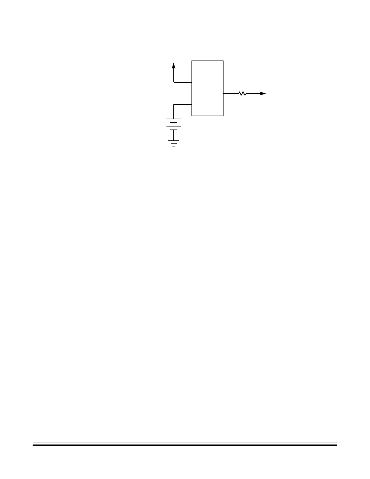
4.8-V
NiCd
Operating Modes and On-Chip Memory
Memory Map
V
DD
MAX
690
V
DD
V
OUT
V
BATT
+
4.7 k
TO MODB/V
OF M68HC11
STBY
Figure 4-8. RAM Standby MODB/V
Connections
STBY
The bootload er program is contained in the internal boo tstrap ROM. This
ROM, which appears as internal memory space at locations
$BF00–$BFFF, is enabled only if the MCU is reset in special bootstrap
mode.
In expanded modes, the ROM/EPROM/OTPROM (if present) is enabled
out of reset and located at the top of the memory map if the RO MON bit
in the CONFIG register i s set. ROM or EPROM is enabled out of rese t in
single-chip and bootstrap modes, regardless of the state of ROMON.
For devices with 512 bytes of EEPROM, the EEPROM is located at
$B600–$B7FF and has the same read cycle time as the internal ROM.
The 512 bytes of EEPROM cannot be remapped to other locations.
For the MC6 8HC811E 2, EEP ROM is l oca ted a t $F 800–$ FFFF and can
be remapped to any 4-Kbyte boundary. EEPROM mapping control bits
(EE[3:0] in CONFIG) determine the location of the 2048 bytes of
EEPROM and are present only on the MC68HC811E2. Refer to
4.4.3.1 System Configuration Register for a description of the
MC68HC811E2 CONFIG register.
EEPROM can be programmed or erased by software and an on-chip
charge pump , allow ing EE PRO M chan ges us in g the single VDD supply.
MC68HC11E Family — Rev. 4 Technical Data
MOTOROLA Operating Modes and On-Chip Memo ry 81

Operating Modes and On-Chip Memory
4.4.2 Mode Selection
The four mode variations are selected by the logic states of the MODA
and MODB pins during reset. The MODA and MODB logic levels
determine the logic state of SMOD and the MDA control bits in the
highest priority I-bit interrupt and miscellaneous (HPRIO) register.
After reset is released, the mode select pins no longer influence the
MCU operating mode. In single-chip operating mode, the MODA pin is
connected to a logic level 0. In expanded mode, MODA is normally
connected to VDD through a pullup resistor of 4.7 kΩ. The MODA pin
also functions as the load instruction register LIR
not in reset. The open-drain active low LIR
the first E cycle of each instruction. The MODB pin also functions as
standby power input (V
maintained in absence of V
pin when the MCU is
output pin drives low during
), which allows RAM contents to be
STBY
.
DD
Refer to Tabl e 4-1, whic h is a summa ry of mode pin opera tion, the mode
control bits, and the four operating modes.
Table 4-1. Hardware Mode Select Summary
Input Levels
at Reset
MODB MODA RBOOT SMOD MDA
1 0 Single chip 0 0 0
1 1 Expanded 0 0 1
00Bootstrap110
01Special test011
Mode
Control Bits in HPRIO
(Latched at Reset)
A normal mode is selected when MODB is logic 1 during reset. One of
three reset vectors is fetched from address $FFFA–$FFFF , and program
execution begins from the address indicated by this vector. If MODB is
logic 0 during reset, the special mode reset vector is fetched from
addresses $BFFA–$BFFF, and software has access to special test
features. Refer to Section 5. Resets and Interrupts.
Technical Data MC68HC11E Family — Rev. 4
82 Operating Modes and On-Chip Memory MOTOROLA
Address: $103C
Bit 7 6 5 4 3 2 1 Bit 0
Operating Modes and On-Chip Memory
Memory Map
Read:
Write:
Resets:
Single chip:00000110
Expanded: 0 0 1 0 0110
Bootstrap:11000110
Test:01110110
1. The reset values depend on the mode selected at the RESET pin rising edge.
RBOOT
(1)
SMOD
(1)
MDA
(1)
IRV(NE)
(1)
PSEL3 PSEL2 PSEL1 PSEL0
Figure 4-9. Highest Priority I-Bit Interrupt and Miscellaneous
Register (HPRIO)
RBOOT — Read Bootstrap ROM Bit
Valid only when S MOD is set (bootstrap o r special test mode); ca n be
written only in special modes
0 = Bootloader ROM disabled and not in map
1 = Bootloader ROM enabled and in map at $BE00–$BFFF
SMOD and MDA — Special Mode S elect and Mode Select A Bits
The initial value of SMOD is the inverse of the logic level present on
the MODB pin at the rising edge of reset. The initial value of MDA
equals the logic level present on the MODA pin at the rising edge of
reset. These two bits can be read at any time. They can be written
anytime in special modes. MDA can be written only once in normal
modes. SMOD cannot be set once it has been cleared.
Input
Mode
MODB MODA SMOD MDA
1 0 Single chip 0 0
1 1 Expanded 0 1
0 0 Bootstrap 1 0
0 1 Special test 1 1
MC68HC11E Family — Rev. 4 Technical Data
Latched at Reset
MOTOROLA Operating Modes and On-Chip Memo ry 83

Operating Modes and On-Chip Memory
IRV(NE) — Internal Read Visibility (Not E) Bit
IRVNE can be written once i n any mode. In expanded modes, IRV NE
determines whether IRV is on or off. In special test mode, IRVNE is
reset to 1. In all other modes, IRVNE is reset to 0. For the
MC68HC811E2, this bit is IRV and only controls the internal read
visibility function.
0 = No internal read visibility on external bus
1 = Data from internal reads is driven out the external data bus.
In single-chip modes this bit determines whether the E clock drives
out from the chip. For the MC68HC81 1E2, this bit has no mea ning or
effect in single-chip and bootstrap modes.
0 = E is driven out from the chip.
1 = E pin is driven low. Refer to the following table.
Mode
Single chip 0 On Off E Once
Expanded 0 On Off IRV On ce
Bootstrap 0 On Off E Once
Special test 1 On On IRV Once
IRVNE Out
of Reset
E Clock Out
of Reset
IRV Out
of Reset
IRVNE
Affects Only
IRVNE Can
Be Written
PSEL[3:0] — Priority Select Bits
Refer to Section 5. Resets and Interrupts.
Technical Data MC68HC11E Family — Rev. 4
84 Operating Modes and On-Chip Memory MOTOROLA

4.4.3 System Initialization
Registers and bits t hat control initialization and the bas ic operation of the
MCU are protected against writes except under special circumstances.
Table 4-2 lists registers that can be written only once after reset or that
must be written within the first 64 cycles after reset.
Table 4-2. Write Access Limited Registers
Operating Modes and On-Chip Memory
Memory Map
Operating
Mode
SMOD = 0 $x024 Timer interrupt mask 2 (TMSK2) Bits [1:0], once only Bits [7:2]
SMOD = 1 $x024 T imer interru p t mask 2 (TMSK2) — All, set or clear
Register
Address
$x035 B lo ck protect register (BPROT) Clear bits, once o nly S et bits only
$x039
$x03C
$x03D RAM and I/O map register (INI T) Yes, once only —
$x035 B lo ck protect register (BPROT) — All, set or clear
$x039
$x03C
$x03D RAM and I/O map register (INIT) — All, set or clear
System configuration
options (OPTION)
Highest priority I-bit interru pt
and miscellaneous (HPRIO)
System configuration options
(OPTION)
Highest priority I-bit interrupt and
miscellaneous (HPRIO)
Register Nam e
Must be Written
in First 64 Cycles
Bits [5:4], bits [2:0],
once only
See HPRIO
description
— All, set or clear
See HPRIO
description
Write
Anytime
Bits [7:6], bit 3
See HPRIO
description
See HPRIO
description
MC68HC11E Family — Rev. 4 Technical Data
MOTOROLA Operating Modes and On-Chip Memo ry 85

Operating Modes and On-Chip Memory
4.4.3.1 System Configuration Register
The system configuration register (CONFIG) consists of an EEPROM
byte and static lat ches th at control th e startup co nfiguration o f the MC U.
The contents of the EEPROM byte are transferred into static working
latches during rese t sequ ences. The operation of the MC U is co ntrolled
directly by these latches and not by CONFIG itself. In normal modes,
changes to CONFIG do not affect operation of the MCU until after the
next reset sequen ce. When pr ogr amm ing, the C ONF IG reg ister it self is
accessed. When the CONFIG register is read, the static latches are
accessed. See 4.6.1 EEPR OM and CONFIG Programming and
Erasure for information on modifying CONFIG.
To take full advantage of the MCU’s functionality, customers can
program the CONFIG register in bootstrap mode. This can be
accomplished by setting the mode pins to logic 0 and downloading a
small program to internal RAM. For more information, Motorola
application note AN1060 enti tled M68HC11 Boo tst ra p M ode has been
included at the back of this document. The downloadable talker will
consist of:
• Bulk erase
• Byte programming
• Communication server
All of this functionality is provided by PCbug11 which can be found on
the Motorola Web site at http://www.motorola.com/semicon ductors/.
For more i nformation on using PCb ug11 to pr ogram an E-series d evice,
Motorola engi neering bulletin EB296 entitled Programming
MC68HC711E9 Devices with PCbug11 and the M68HC11EVBU has
been included at the back of this document.
NOTE: The CONFIG register on the 68HC11 is an EEPROM cell and must be
programmed accordingly.
Operation of the CONFIG register in the MC68HC811E2 differs from
other devices in the M68HC11 E series. See Figure 4-10 and
Figure 4-11.
Technical Data MC68HC11E Family — Rev. 4
86 Operating Modes and On-Chip Memory MOTOROLA

Address: $103F
Bit 7654321Bit 0
Operating Modes and On-Chip Memory
Memory Map
Read:
Write:
Resets:
Single chip:0000UU1U
Bootstrap:0000UU(L)UU
Expanded: 00001UUU
Test:00001U(L)UU
= Unimplemented
U indicates a previously programmed bit. U(L) indicates that the bit resets to the logic level held in the latch
prior to reset, but the function of COP is controlled by the DISR bit in TEST1 register.
NOSEC NOCOP ROMON EEON
Figure 4-10. System Configuration Register (CONFIG)
Address: $103F
Bit 7654321Bit 0
Read:
EE3 EE2 EE1 EE0 NOSEC NOCOP
Write:
EEON
Resets:
Single chip:1111UU11
Bootstrap:1111UU(L)11
Expanded: UUUU1U1U
Test:UUUU1U(L)10
= Unimplemented
U indicates a previously programmed bit. U(L) indicates that the bit resets to the logic level held in the latch
prior to reset, but the function of COP is controlled by the DISR bit in TEST1 register.
Figure 4-11. MC68HC811E2 System Configuration Register (CONFIG)
MC68HC11E Family — Rev. 4 Technical Data
MOTOROLA Operating Modes and On-Chip Memo ry 87

Operating Modes and On-Chip Memory
EE[3:0] — EEPROM Mapping Bits
EE[3:0] apply only to MC68HC811E2 and allow the 2048 bytes of
EEPROM to be remapped to any 4-Kbyte boundary. See Table 4-3.
Table 4-3. EEPROM Mapping
EE[3:0] EEPROM Location
0 0 0 0 $0800 –$0FFF
0 0 0 1 $1800 –$1FFF
0 0 1 0 $2800 –$2FFF
0 0 1 1 $3800 –$3FFF
0 1 0 0 $4800 –$4FFF
0 1 0 1 $5800 –$5FFF
0 1 1 0 $6800 –$6FFF
0 1 1 1 $7800 –$7FFF
1 0 0 0 $8800 –$8FFF
1 0 0 1 $9800 –$9FFF
1 0 1 0 $A800–$AFFF
1 0 1 1 $B800–$BFFF
1 1 0 0 $C800–$CFFF
1 1 0 1 $D800–$DFFF
1 1 1 0 $E800–$EFFF
1 1 1 1 $F800–$FFFF
NOSEC — Security Disable Bit
NOSEC is invalid unless th e secur i ty mask o ption is spec if ied befo re
the MCU is manufactured. If the security mask option is omitted
NOSEC always reads 1. The enhanced security feature is available
in the MC68S711 E9 MCU. The enhancement to the standard security
feature protects the EPROM as well as RAM and EEPROM.
0 = Security enabled
1 = Security disabled
NOCOP — COP System Disable Bit
Refer to Section 5. Resets and Interrupts.
1 = COP disabled
0 = COP enabled
Technical Data MC68HC11E Family — Rev. 4
88 Operating Modes and On-Chip Memory MOTOROLA

ROMON — ROM/EPROM/OTPR OM Enable Bit
When this bit is 0, the ROM or EPROM is disabled and that memory
space becomes extern ally addresse d. In single-ch ip mode, RO MO N
is forced to 1 to enable ROM/EPROM regardless of the state of the
ROMON bit.
0 = ROM disabled from the memory map
1 = ROM present in the memory map
EEON — EEPROM Enable Bit
When this bit is 0, the EEPROM is disabled and that memory space
becomes externally addressed .
0 = EEPROM removed from the memory map
1 = EEPROM present in the memory map
4.4.3.2 RAM and I/O Mapping Register
Operating Modes and On-Chip Memory
Memory Map
The internal registers used to control the operation of the MCU can be
relocated on 4-Kbyte bound ari es within the memory space with the use
of the RAM and I/O mapping register (INIT). This 8-bit special-purpose
register can change the default locations of the RAM and control
registers within the MCU memory map. It can be written only once withi n
the first 64 E-clock cycles after a reset in normal modes, and then it
becomes a read-only register.
Address: $103D
Bit 7654321Bit 0
Read:
Write:
Reset:00000001
RAM3 RAM2 RAM1 RAM0 REG3 REG2 REG1 REG0
Figure 4-12. RAM and I/O Mapping Register (INIT)
RAM[3:0] — RAM Map Position Bits
These four bits, which specify the up per hexadecimal digit of the RAM
address, control position of RAM in the memory map. RAM can be
positioned at the begi n ning of any 4 -K byte p age in the m emo ry ma p.
It is initialized to address $0000 out of reset. Refer to Table 4-4.
MC68HC11E Family — Rev. 4 Technical Data
MOTOROLA Operating Modes and On-Chip Memo ry 89

Operating Modes and On-Chip Memory
REG[3:0] — 64-Byte Register Block Position
These four bits sp ecify th e upper hexadecimal d igit of the addr ess for
the 64-byte block of internal registers. The register block, positioned
at the beginnin g of any 4-Kb yte page in the m emory map, is i nitialized
to address $1000 out of reset. Refer to Table 4-5.
Table 4-4. RAM Mapping Table 4-5. Register Mapping
RAM[3:0] Addr ess REG[3:0] Address
0000 $0000–$0xFF 0000 $0000–$003F
0001 $1000–$1xFF 0001 $1000–$103F
0010 $2000–$2xFF 0010 $2000–$203F
0011 $3000–$3xFF 0011 $3000–$303F
0100 $4000–$4xFF 0100 $4000–$403F
0101 $5000–$5xFF 0101 $5000–$503F
0110 $6000–$6xFF 0110 $6000–$603F
0111 $7000–$7xFF 0111 $7000–$703F
1000 $8000–$8xFF 1000 $8000–$803F
1001 $9000–$9xFF 1001 $9000–$903F
1010 $A000–$AxFF 1010 $A000–$A03F
1011 $B000–$BxFF 1011 $B000–$B03 F
1100 $C 000–$CxFF 1100 $C000–$C03F
1101 $D 000–$DxFF 1101 $D000–$D03F
1110 $E000–$Ex FF 1110 $E000–$E03F
1111 $F000–$FxFF 1111 $F000–$F03F
Technical Data MC68HC11E Family — Rev. 4
90 Operating Modes and On-Chip Memory MOTOROLA

4.4.3.3 System Configuration Options Register
The 8-bit, special-purpose system configuration options register
(OPTION) sets internal system configuration options during initialization.
The time protected contro l bits, IRQE, DLY , and CR[1:0], can be written
only once after a r eset and then th ey become re ad-only . This mini mizes
the possibility of an y acciden tal chan ges to the system configuration.
Address: $1039
Bit 7654321Bit 0
Operating Modes and On-Chip Memory
Memory Map
Read:
ADPU CSEL IRQE
Write:
Reset:00010000
1. Can be written only once in first 64 cycle s out of reset in normal modes or at any time during
special modes.
= Unimplemented
(1)
DLY
(1)
CME CR1
(1)
CR0
(1)
Figure 4-13. System Configuration Options Register (OPTION)
ADPU — Analog-to-Digital Converter Power-Up Bit
Refer to Section 10. Analog-to-Digital (A/D) Converter.
CSEL — Clock Select Bit
Selects alternate clock source for on-chip EEPROM charge pump.
Refer to 4.6.1 EEPROM and CONFIG Programming and Erasure
for more information on EEPROM use.
CSEL also selects the clock source for the A/D converter, a function
discussed in Section 10. Analog-to-Digital (A/D) Converter.
IRQE — Configure IRQ
for Edge-Sensitive Only Operation Bit
Refer to Section 5. Resets and Interrupts.
DLY — Enable Oscillator Startup Delay Bit
0 = The oscillator startup delay coming out of stop mode is
bypassed and the MCU resumes proce ssing within about four
bus cycles.
1 = A delay of approximately 4000 E-clock cycles is impose d as the
MCU is started up from the stop power-saving mode. This
delay allows the crystal oscillator to stabilize.
MC68HC11E Family — Rev. 4 Technical Data
MOTOROLA Operating Modes and On-Chip Memo ry 91

Operating Modes and On-Chip Memory
CME — Clock Monitor Enable Bit
Refer to Section 5. Resets and Interrupts.
Bit 2 — Not implemented
Always reads 0
CR[1:0] — COP Timer Rate Select Bits
The internal E clock is divided by 215 before it enters the COP
watchdog system. These control bits determine a scaling factor for
the watchdog timer. Refer to Section 5. Resets and Interrupts.
4.5 EPROM/OTPROM
Certain devices in the M68HC11 E series include on-chip
EPROM/OTPROM. For instance:
• The MC68HC711E9 devices contain 12 Kbytes of on-chip
EPROM (OTPROM in non-windowed package).
• The MC68HC711E20 has 20 Kbytes of EPROM (OTPROM in
non-windowed package).
• The MC68HC711E32 has 32 Kbytes of EPROM (OTPROM in
non-windowed package).
Standard MC68 HC71E9 and MC68HC711E20 devi ces are shipped with
the EPROM/OTPROM contents erased (all 1s). The programming
operation programs 0s. Windowed devices must be erased using a
suitable ul traviolet light sour ce before reprogramm ing. Depending o n the
light source, erasing can take from 15 to 45 minutes.
Using the on-chip EPROM/OTPROM programming feature requires an
external 12-volt nominal power supply (V
). Normal programming is
PPE
accomplished using the EPROM/OTPROM programming register
(PPROG).
PPROG is the combined EPROM/OTPROM and EEPROM
programming reg i ster on all devi ces wi th EP ROM/OT PRO M excep t the
MC68HC711E20 . For the MC68 HC711E20, th ere is a se parate reg ister
for EPROM/OTPROM programming called the EPROG register.
Technical Data MC68HC11E Family — Rev. 4
92 Operating Modes and On-Chip Memory MOTOROLA

As described in the following subsections, these two methods of
programming and verifying EPROM are possible:
• Programming an individual EPROM address
• Programming the EPROM with downloaded data
4.5.1 Programming an Individual EPROM Address
In this method, the MC U programs its own EPROM by controlling the
PPROG register (EPROG in MC68HC711E20). Use these procedures
to program the EPROM through the MCU with:
• The ROMON bit set in the CONFIG register
• The 12-volt nominal programming voltage present on the
XIRQ/V
PPE
pin
Operating Modes and On-Chip Memory
EPROM/OTPROM
• The IRQ
pin must be pulled high.
NOTE: Any operating mode can be used.
This example applies to all devices with EPROM/OTPROM except for
the MC68HC711E20.
EPROG LDAB #$20
STAB $103B Set ELAT bit in (EPGM = 0) to enable
STAA $0,X Store data to EPROM address
LDAB #$21
STAB $103B Set EPGM bit with ELAT = 1 to enable
JSR DLYEP Delay 2–4 ms
CLR $103B Turn off programming voltage and set
This example applies only to MC68HC711E20.
EPROG LDAB #$20
STAB $1036 Set ELAT bit (EPGM = 0) to enable
STAA $0,X Store data to EPROM address
LDAB #$21
STAB $1036 Set EPGM bit with ELAT = 1 to enable
JSR DLYEP Delay 2–4 ms
CLR $1036 Turn off programming voltage and set
EPROM latches.
EPROM programming voltage
to READ mode
EPROM latches.
EPROM programming voltage
to READ mode
MC68HC11E Family — Rev. 4 Technical Data
MOTOROLA Operating Modes and On-Chip Memo ry 93

Operating Modes and On-Chip Memory
4.5.2 Programming the EPROM with Downloaded Data
When using thi s metho d, th e E PRO M is prog ramm ed by software while
in the spe cial te st or b ootstr ap mode s. Use r-de v eloped so ftware can be
uploaded through the SCI or a ROM-resident EPROM programming
utility can be used. The 12-volt nominal programming voltage must be
present on the XIRQ/V
3-byte program co nsis ting o f a singl e jump instructi o n to $ BF00. $B F00
is the starting address of a resident EPROM programming utility. The
utility program sets the X and Y index registers to default values, then
receives progr amming data from an e xternal host, and puts it in EPROM.
The value in IX determines programming delay time. The value in IY is
a pointer to the first address in EPROM to be programmed
(default = $D000).
When the utility program is ready to receive programmin g data, it sends
the host the $FF character. Then it waits. When the host sees the $FF
character, the EPROM programming data is sent, starting with the first
location in the EPROM array. After the last byte to be programmed is
sent and the corresponding verification data is returned, the
programming operation is terminated by resetting the MCU.
pin. To use the resident utility, bootload a
PPE
For more information, Motorola application note AN1060 entitled
M68HC11 Bootstrap Mode has been included at the back of this
document.
4.5.3 EPROM and EEPROM Programming Control Register
The EPROM and EEPROM programming control register (PPROG)
enables the EPROM programming voltage and controls the latching of
data to be programmed.
• For MC68HC711E9, PPROG is also the EEPROM programming
control register.
• For the MC68HC711E20, EPROM programming is controlled by
the EPROG register and EEPROM programming is controlled by
the PPROG register.
Technical Data MC68HC11E Family — Rev. 4
94 Operating Modes and On-Chip Memory MOTOROLA

Address: $103B
Bit 7654321Bit 0
Operating Modes and On-Chip Memory
EPROM/OTPROM
Read:
ODD EVEN ELAT
Write:
Reset:00000000
1. MC68HC711E9 only
(1)
BYTE ROW ERASE EELAT EPGM
Figure 4-14. EPROM and EEPROM Programming
Control Register (PPROG)
ODD — Program Odd Rows in Half of EEPROM (Test) Bit
Refer to 4.6 EEPROM.
EVEN — Program Even Rows in Half of EEPROM (Test) Bit
Refer to 4.6 EEPROM.
ELAT — EPROM/OTPROM Latch Control Bit
When ELAT = 1, writes to EPROM cause address and data to be
latched and the EPROM/OTPROM cannot be read. ELAT can be
read any time. ELAT can be wri tten any time except when EPGM = 1;
then the write to ELAT is disabled.
0 = EPROM address and data bus configured for normal reads
1 = EPROM address and data bus configured for programming
For the MC68HC711E9:
a. EPGM enables t he high voltage necessary for both EEPROM
and EPROM/OTPROM programming.
b. ELAT and EELAT are mutually exclusive and cannot both
equal 1.
BYTE — Byte/Other EEPROM Erase Mode Bit
Refer to 4.6 EEPROM.
ROW — Row/All EEPROM Erase Mode Bit
Refer to 4.6 EEPROM.
MC68HC11E Family — Rev. 4 Technical Data
MOTOROLA Operating Modes and On-Chip Memo ry 95

Operating Modes and On-Chip Memory
ERASE — Erase Mode Select Bit
Refer to 4.6 EEPROM.
EELAT — EEPROM Latch Control Bit
Refer to 4.6 EEPROM.
EPGM — EPROM/OTPROM/EEPROM Programming
Voltage Enable Bit
EPGM can be read a ny time an d can be written only when ELAT = 1
(for EPROM/OTPROM programming) or when EELAT = 1 (for
EEPROM programming).
0 = Programming voltage to EPROM/OTPROM/EEPROM array
disconnected
1 = Programming voltage to EPROM/OTPROM/EEPROM array
connected
Address: $1036
Bit 7654321Bit 0
Read:
Write:
MBE
Reset:00000000
= Unimplemented
ELAT EXCOL EXROW T1 T0 PGM
Figure 4-15. MC68HC711E20 EPROM Programming
Control Register (EPROG)
MBE — Multiple-Byte Programming Enable Bit
When multiple-byte programming is enabled, address bit 5 is
considered a don’t care so that bytes with address bit 5 = 0 and
address bit 5 = 1 both get program med. MBE can be rea d in any mode
and always reads 0 in normal modes. MBE can be w ritten only in
special modes.
0 = EPROM array configured for normal programming
1 = Program two bytes with the same data
Bit 6 — Unimplemented
Always reads 0
Technical Data MC68HC11E Family — Rev. 4
96 Operating Modes and On-Chip Memory MOTOROLA

Operating Modes and On-Chip Memory
EPROM/OTPROM
ELAT — EPROM/OTPROM Latch Control Bit
When ELAT = 1, writes to EPROM cause address and data to be
latched and the EPROM/OTPROM cannot be read. ELAT can be
read any time. ELAT can be written any time except when PGM = 1;
then the write to ELAT is disabled.
0 = EPROM/O TPROM address and data b us configured for normal
reads
1 = EPROM/OTPROM address and data bus configured for
programming
EXCOL — Select Extra Colum ns Bit
0 = User array sel ected
1 = User array is disabled and extr a column s are accessed at bits
[7:0]. Addresses use bits [13:5] and bits [4:0] are don’t care.
EXCOL can be read and written only in special modes and
always returns 0 in normal modes.
EXROW — Select Extra Rows Bit
0 = User array sel ected
1 = User array is disabled and two extra rows are available.
Addresses use bits [7:0] and bits [1 3:8] are don’t care. EXROW
can be read and written only in special modes and always
returns 0 in normal modes.
T[1:0] — EPROM Test Mode Select Bits
These bits allow selection of either gate stress or drain stress test
modes. They can be read and written only in special modes and
always read 0 in normal modes.
T1 T0 Function Selected
0 0 Normal mode
0 1 Reserved
1 0 Gate stress
1 1 Drain stress
MC68HC11E Family — Rev. 4 Technical Data
MOTOROLA Operating Modes and On-Chip Memo ry 97

Operating Modes and On-Chip Memory
PGM — EPROM Programming Voltage Enable Bit
PGM can be read any time and can be written only when ELAT = 1.
0 = Programming voltage to EPROM array disconnected
1 = Programming voltage to EPROM array connected
4.6 EEPROM
Some E-series devices contain 512 bytes of on-chip EEPROM. The
MC68HC811E2 contains 2048 bytes of EEPROM with selectable base
address. All E-series devices contain the EEPROM-based CONFIG
register.
4.6.1 EEPROM and CONFIG Programming and Erasure
The erased state of an EEPROM bit is 1. During a read operation, bit
lines are precharge d to 1. The floating gate devices of pro grammed bits
conduct and pull the bit lines to 0. Unprogrammed bits remain at the
precharged le vel and are r ead as 1s. P ro grammi ng a bit to 1 cause s no
change. Programming a bit to 0 changes the bit so that subsequent
reads return 0.
When appropriate bits in the BPROT register are cleared, the PPROG
register controls programming and erasing the EEPROM. The PPROG
register can be read or written at any time, but logic enforces defined
programming and erasing sequences to prevent unintentional changes
to EEPROM data. When the EELAT bit in the PPROG registe r is cleared,
the EEPROM can be read as if it were a ROM.
The on-chip charge pump that generates the EEPROM programming
voltage from V
uses MOS capacitors, which are relatively small in
DD
value. The efficiency of this charge pump and its drive capability are
affected by the level of VDD and the frequency of the driving clock. The
load depends on the number of bits being programmed or erased and
capacitances in the EEPROM array.
The clock source driving the charg e pump is software sel ectable. When
the clock select (CSEL) bit in the OPTION register is 0, the E clock is
Technical Data MC68HC11E Family — Rev. 4
98 Operating Modes and On-Chip Memory MOTOROLA

used; when CSEL is 1, an on-chip resistor-capacitor (RC) oscillator is
used.
The EEPROM programming voltage power supply voltage to the
EEPROM array is not enabled until there has been a write to PPROG
with EELAT set and PGM cleared. This must be foll owed by a write to a
valid EEPROM location or to the CONFIG address, and then a write to
PPROG with both the EELAT and EPGM bits set. Any attempt to set
both EELAT and EPGM during the same write operation results in
neither bit being set.
4.6.1.1 Block Protect Register
This register prevents inadvertent writes to both the CONFIG register
and EEPROM. The active bits in this register are initialized to 1 out of
reset and can be cleared only during the first 64 E-clock cycles after
reset in the normal modes. When these bits are cl eared, the associated
EEPROM section and the CONFIG register can be programmed or
erased. EEPROM i s o nly visi ble if th e E EON bit in the CO NFIG registe r
is set. The bits in the BPROT register can be written to 1 at any time to
protect EEPROM and the CONFIG register. In test or bootstrap mode s,
write protection is inhibited and BPROT can be written repeatedly.
Address ranges for protected areas of EEPROM differ significantly for
the MC68HC811E2. Refer to Figure 4-16.
Operating Modes and On-Chip Memory
EEPROM
Address: $1035
Bit 7654321Bit 0
Read:
PTCON BPRT3 BPRT2 BPRT1 BPRT0
Write:
Reset:00011111
= Unimplemented
Figure 4-16. Block Protect Register (BPROT)
Bits [7:5] — Unimplemented
Always read 0
MC68HC11E Family — Rev. 4 Technical Data
MOTOROLA Operating Modes and On-Chip Memo ry 99
Operating Modes and On-Chip Memory
PTCON — Protect CONFIG Register Bit
0 = CONFIG register can be programmed or erased normally.
1 = CONFIG register cannot be programmed or erased.
BPRT[3:0] — Block Protect Bits for EEPROM
When set, these bits protect a block of EEPROM from being
programmed or electronically erased. Ultraviolet light, however, can
erase the entire EEPROM contents regardless of BPRT[3:0]
(windowed packages only). Refer to Table 4-6 and Table 4-7.
When cleared, BPRT[3:0] allow programming and erasure of the
associated block.
Table 4-6. EEPROM Block Protect
Bit Name Block Protected Block Size
BPRT0 $B600–$B61F 32 bytes
BPRT1 $B620–$B65F 64 bytes
BPRT2 $B660–$B6DF 128 bytes
BPRT3 $B6E0–$B 7FF 288 by t es
Table 4-7. EEPROM Block Protect in MC68HC811E2 MCUs
Bit Name Block Protected Block Size
BPRT0
BPRT1
BPRT2
BPRT3
1. x is determined by the value of EE[3 :0] in CONFIG register. Refer to
Figure 4-13.
$x800–$x9FF
$xA00–$xBFF
$xC00–$xDFF
$xE00–$xFFF
(1)
(1)
(1)
(1)
512 bytes
512 bytes
512 bytes
512 bytes
Technical Data MC68HC11E Family — Rev. 4
100 Operating Modes and On-Chip Memory MOTOROLA
 Loading...