

Motorola MC68HCP11A1P, MC68HCP11A1VFN, MC68HCP11A1VP, MC68HCP11A1MFN, MC68HC11A8FN1 Datasheet
...
MOTOROLA
Order this document
by MC68HC11A8TS/D
SEMICONDUCTOR
TECHNICAL DATA
MC68HC11A8
MC68HC11A1
MC68HC11A0
Technical Summary
8-Bit Microcontrollers
1 Introduction
The MC68HC11A8, MC68HC11A1, and MC68HC11A0 high-performance microcontroller units (MCUs)
are based on the M68HC11 Family. These high speed, low power consumption chips have multiplexed
buses and a fully static design. The chips can operate at frequencies from 3 MHz to dc. The three MCUs
are created from the same masks; the only differences are the value stored in the CONFIG register, and
whether or not the ROM or EEPROM is tested and guaranteed.
For detailed information about specific characteristics of these MCUs, refer to the
Manual
(M68HC11RM/AD).
M68HC11 Reference
1.1 Features
• M68HC11 CPU
• Power Saving STOP and WAIT Modes
• 8 Kbytes ROM
• 512 Bytes of On-Chip EEPROM
• 256 Bytes of On-Chip RAM (All Saved During Standby)
• 16-Bit Timer System
— 3 Input Capture Channels
— 5 Output Compare Channels
• 8-Bit Pulse Accumulator
• Real-Time Interrupt Circuit
• Computer Operating Properly (COP) Watchdog System
• Synchronous Serial Peripheral Interface (SPI)
• Asynchronous Nonreturn to Zero (NRZ) Serial Communications Interface (SCI)
• 8-Channel, 8-Bit Analog-to-Digital (A/D) Converter
• 38 General-Purpose Input/Output (I/O) Pins
— 15 Bidirectional I/O Pins
— 11 Input-Only Pins and 12 Output-Only Pins (Eight Output-Only Pins in 48-Pin Package)
• Available in 48-Pin Dual In-Line Package (DIP) or 52-Pin Plastic Leaded Chip Carrier (PLCC)
This document contains information on a new product. Specifications and information herein are subject to change without notice.
© MOTOROLA INC., 1991, 1996

Table 1 MC68HC11Ax Family Members
Device Number ROM EEPROM RAM CONFIG* Comments
MC68HC11A8 8K 512 256 $0F Family built around this device
MC68HC11A1 0 512 256 $0D ROM disabled
MC68HC11A0 0 0 256 $0C ROM and EEPROM disabled
Table 2 Ordering Information
Package Temperature CONFIG Description MC Order Number
48-Pin Plastic DIP
(P suffix)
–40 ° to + 85 ° C $0F BUFFALO ROM MC68HC11A8P1
–40 ° to + 85 ° C $0D No ROM MC68HC11A1P
–40 ° to + 105 ° C $0D No ROM MC68HC11A1VP
–40 ° to + 125 ° C $0D No ROM MC68HC11A1MP
–40 ° to + 85 ° C $09 No ROM, COP On MC68HCP11A1P
–40 ° to + 105 ° C $09 No ROM, COP On MC68HCP11A1VP
–40 ° to + 125 ° C $09 No ROM, COP On MC68HCP11A1MP
–40 ° to + 85 ° C $0C No ROM, No EEPROM MC68HC11A0P
52-Pin PLCC
(FN suffix)
–40 ° to + 85 ° C $0F BUFFALO ROM MC68HC11A8FN1
–40 ° to + 85 ° C $0D No ROM MC68HC11A1FN
–40 ° to + 105 ° C $0D No ROM MC68HC11A1VFN
–40 ° to + 125 ° C $0D No ROM MC68HC11A1MFN
–40 ° to + 85 ° C $09 No ROM, COP On MC68HCP11A1FN
–40 ° to + 105 ° C $09 No ROM, COP On MC68HCP11A1VFN
–40 ° to + 125 ° C $09 No ROM, COP On MC68HCP11A1MFN
–40 ° to + 85 ° C $0C No ROM, No EEPROM MC68HC11A0FN
MOTOROLA MC68HC11A8
2 MC68HC11A8TS/D

TABLE OF CONTENTS
Section Page
1 Introduction...............................................................................................................................................1
1.1 Features ..........................................................................................................................................1
2 Operating Modes and Memory Maps.......................................................................................................6
2.1 Memory Maps ..................................................................................................................................7
3 Resets and Interrupts.............................................................................................................................13
4 Electrically Erasable Programmable Read-Only Memory (EEPROM) ...................................................17
5 Parallel Input/Output...............................................................................................................................19
6 Serial Communications Interface (SCI)..................................................................................................23
7 Serial Peripheral Interface (SPI).............................................................................................................29
8 Main Timer..............................................................................................................................................32
9 Pulse Accumulator..................................................................................................................................38
10 Analog-to-Digital Converter..................................................................................................................41
MC68HC11A8 MOTOROLA
MC68HC11A8TS/D 3

XTAL
EXTAL
E
PA7
PA6
PA5
PA4
PA3
PA2
PA1
PA0
A7/D7
A6/D6
A5/D5
A4/D4
A3/D3
A2/D2
A1/D1
A0/D0
A15
A14
A13
A12
A11
A10
A9
A8
R/W
AS
PAI/OC1
OC2/OC1
OC3/OC1
PORT A
SINGLE
CHIPEXPANDED
PB7
PB6
PB5
PB4
PB3
PB2
PB1
PB0
PC7
PC6
PC5
PC4
PC3
PC2
PC1
PC0
STRB
STRA
EQUIVALENT TO MC68HC24
OC4/OC1
OC5/OC1
IC1
IC2
IC3
PORT B
PORT C
PORT C DDR
PARALLEL I/O
PULSE
ACCUMULATOR
TIMER
SYSTEM
CPU
HANDSHAKE I/O
COP
PERIODIC
INTERRUPT
BYTES
8
KBYTES
ROM
ADDRESS/DATA BUS
OSCILLATOR
256
RAM
512
BYTES
EEPROM
POWER
INTERRUPT
LOGIC
MODE
SELECT
A/D
CONVERTER
AN7
AN6
AN5
AN4
AN3
AN2
AN1
AN0
SS
SCK
SPI
MOSI
MISO
TxD
SCI
RxD
PORT E
PORT D
PORT D DDR
V
DD
V
SS
IRQ
XIRQ
RESET
MODA/
LIR
MODB/
V
STBY
V
RH
V
RL
PE7
PE6
PE5
PE4
PE3
PE2
PE1
PE0
PD5
PD4
PD3
PD2
PD1
PD0
Figure 1 MC68HC11A8 Block Diagram
MOTOROLA MC68HC11A8
4 MC68HC11A8TS/D

XTAL
PC0/A0/D0
PC1/A1/D1
PC2/A2/D2
PC3/A3/D3
PC4/A4/D4
PC5/A5/D5
PC6/A6/D6
PC7/A7/D7
RESET
XIRQ
IRQ
PD0/RxD
8
9
10
11
12
13
14
15
16
17
18
19
20
STRB/R/W
EXTAL
6
7
212223
E
5
STRA/AS
MODA/LIR
4
3
252627
24
STBY
SS
MODB/V
VRHV
2
52
1
2829303132
RL
V
51
PE7/AN7
PE3/AN3
495047
PE6/AN6
PE2/AN2
48
46
45
44
43
42
41
40
39
38
37
36
35
34
33
PE5/AN5
PE1/AN1
PE4/AN4
PE0/AN0
PB0/A8
PB1/A9
PB2/A10
PB3/A11
PB4/A12
PB5/A13
PB6/A14
PB7/A15
PA0/IC3
DD
V
PD1/TxD
PD2/MISO
PD5/SS
PD4/SCK
PD3/MOSI
PA7/PAI/OC1
PA6/OC2/OC1
PA5/OC3/OC1
PA2/IC1
PA1/IC2
PA3/OC5/OC1
PA4/OC4/OC1
Figure 2 52-Pin PLCC Pin Assignments
MC68HC11A8 MOTOROLA
MC68HC11A8TS/D 5

PA7/PAI/OC1
PA6/OC2/OC1
PA5/OC3/OC1
PA4/OC4/OC1
PA3/OC5/OC1
PA2/IC1
PA1/IC2
PA0/IC3
PB7/A15
PB6/A14
PB5/A13
PB4/A12
PB3/A11
PB2/A10
PB1/A9
PB0/A8
PE0/AN0
PE1/AN1
PE2/AN2
PE3/AN3
V
V
V
MODB/V
STBY
RL
RH
SS
1
2
3
4
5
6
7
8
9
10
11
12
13
14
15
16
17
18
19
20
21
22
23
24
48
47
46
45
44
43
42
41
40
39
38
37
36
35
34
33
32
31
30
29
28
27
26
25
V
DD
PD5/SS
PD4/SCK
PD3/MOSI
PD2/MISO
PD1/TxD
PD0/RxD
IRQ
XIRQ
RESET
PC7/A7/D7
PC6/A6/D6
PC5/A5/D5
PC4/A4/D4
PC3/A3/D3
PC2/A2/D2
PC1/A1/D1
PC0/A0/D0
XTAL
EXTAL
STRB/ R/W
E
STRA/AS
MODA/LIR
Figure 3 48-Pin DIP Pin Assignments
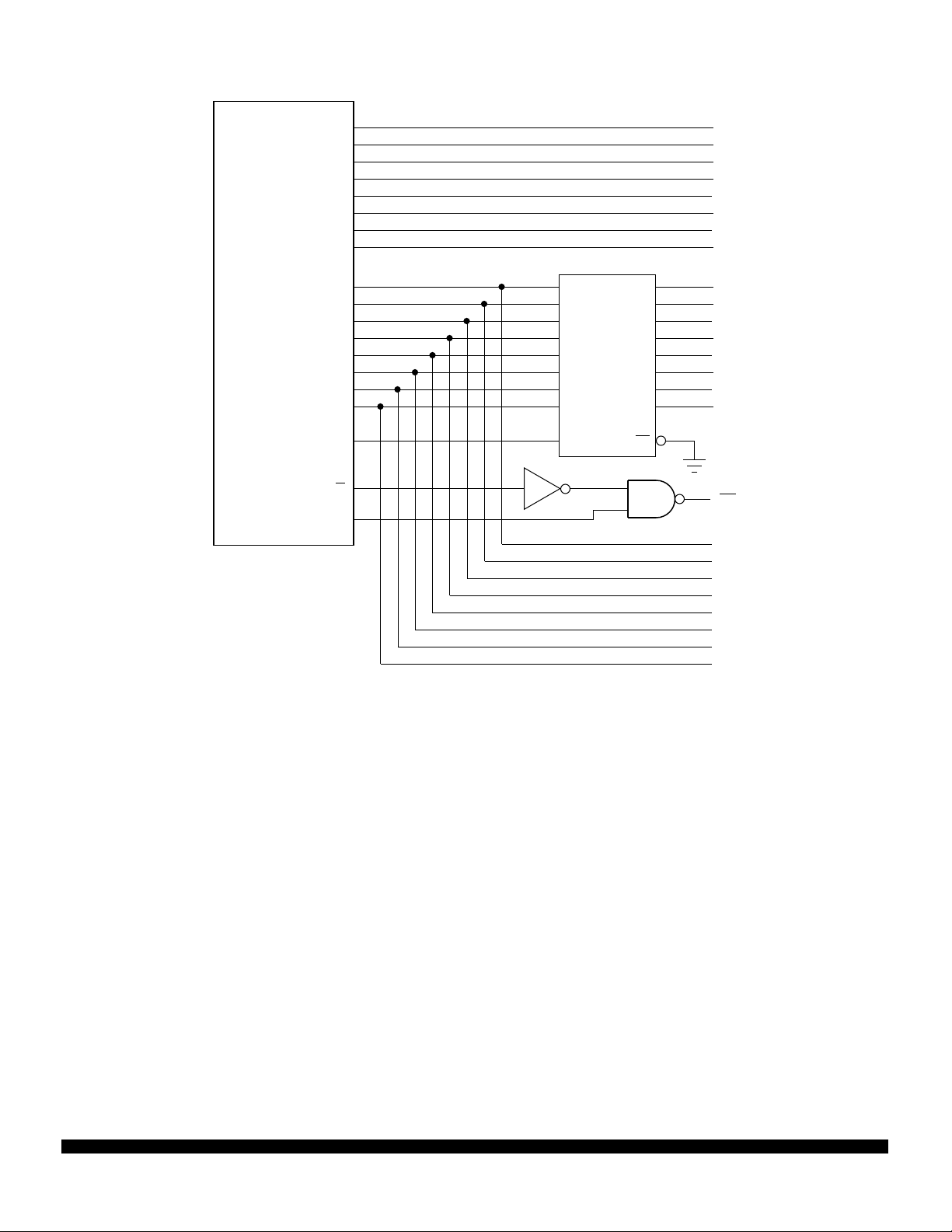
2 Operating Modes and Memory Maps
In single-chip operating mode, the MC68HC11A8 is a monolithic microcontroller without external address or data buses.
In expanded multiplexed operating mode, the MCU can access a 64 Kbyte address space. The space
includes the same on-chip memory addresses used for single-chip mode plus external peripheral and
memory devices. The expansion bus is made up of ports B and C and control signals AS and R/W
address, R/W, and AS signals are active and valid for all bus cycles including accesses to internal memory locations. The following figure illustrates a recommended method of demultiplexing low-order addresses from data at port C.
. The
MOTOROLA MC68HC11A8
6 MC68HC11A8TS/D
MC68HC11A8
PB7
PB6
PB5
PB4
PB3
PB2
PB1
PB0
PC7
PC6
PC5
PC4
PC3
PC2
PC1
PC0
AS
R/W
A15
A14
A13
A12
A11
A10
A9
A8
MC54/74HC373
D1
D2
D3
D4
D5
D6
D7
D8
LE
E
Q1
Q2
Q3
Q4
Q5
Q6
Q7
Q8
OE
A7
A6
A5
A4
A3
A2
A1
A0
WE
D7
D6
D5
D4
D3
D2
D1
D0
Figure 4 Address/Data Demultiplexing
Special bootstrap mode allows special purpose programs to be entered into internal RAM. The bootloader program uses the SCI to read a 256-byte program into on-chip RAM at $0000 through $00FF.
After receiving the character for address $00FF, control passes to the loaded program at $0000.
Special test mode is used primarily for factory testing.
2.1 Memory Maps
Memory locations are the same for expanded multiplexed and single-chip modes. The on-board 256byte RAM is initially located at $0000 after reset. The 64-byte register block originates at $1000 after
reset. RAM and/or the register block can be placed at any other 4K boundary ($x000) after reset by writing an appropriate value to the INIT register. The 512-byte EEPROM is located at $B600 through $B7FF
after reset if it is enabled. The 8 Kbyte ROM is located at $E000 through $FFFF if it is enabled.
Hardware priority is built into the memory remapping. Registers have priority over RAM, and RAM has
priority over ROM. The higher priority resource covers the lower, making the underlying locations inaccessible.
In special bootstrap mode, a bootloader ROM is enabled at locations $BF40 through $BFFF.
In special test and special bootstrap modes, reset and interrupt vectors are located at $BFC0 through
$BFFF.
MC68HC11A8 MOTOROLA
MC68HC11A8TS/D 7

$0000
$1000
$B600
$E000
$FFFF
SINGLE
CHIP
EXT
EXT
EXPANDED
MUX
SPECIAL
BOOTSTRAP
EXTEXT
EXT
EXT
SPECIAL
TEST
0000
256 BYTES RAM
(CAN BE REMAPPED TO ANY
4K PAGE BY THE INIT REGISTER)
00FF
1000
64 BYTE REGISTER BLOCK
(CAN BE REMAPPED TO ANY
4K PAGE BY THE INIT REGISTER)
103F
B600
512 BYTES EEPROM
B7FF
BF40
BOOT
ROM
BFFF
E000
8K ROM
FFFF
BFC0
BFFF
FFC0
FFFF
SPECIAL
MODE
INTERRUPT
VECTORS
NORMAL
MODE
INTERRUPT
VECTORS
Figure 5 Memory Map
MOTOROLA MC68HC11A8
8 MC68HC11A8TS/D

Table 3 MC68HC11A8 Register and Control Bit Assignments (Sheet 1 of 2)
(The register block can be remapped to any 4K boundary.)
Bit 7 654321Bit 0
$1000 PA7 PA6 PA5 PA4 PA3 PA2 PA1 PA0 PORTA
$1001 Reserved
$1002 STAF STAI CWOM HNDS OIN PLS EGA INVB PIOC
$1003 PC7 PC6 PC5 PC4 PC3 PC2 PC1 PC0 PORTC
$1004 PB7 PB6 PB5 PB4 PB3 PB2 PB1 PB0 PORTB
$1005 PCL7 PCL6 PCL5 PCL4 PCL3 PCL2 PCL1 PCL0 PORTCL
$1006 Reserved
$1007 DDC7 DDC6 DDC5 DDC4 DDC3 DDC2 DDC1 DDC0 DDRC
$1008 0 0 PD5 PD4 PD3 PD2 PD1 PD0 PORTD
$1009 0 0 DDD5 DDD4 DDD3 DDD2 DDD1 DDD0 DDRD
$100A PE7 PE6 PE5 PE4 PE3 PE2 PE1 PE0 PORTE
$100B FOC1 FOC2 FOC3 FOC4 FOC5 0 0 0 CFORC
$100C OC1M7 OC1M6 OC1M5 OC1M4 OC1M3 0 0 0 OC1M
$100D OC1D7 OC1D6 OC1D5 OC1D4 OC1D3 0 0 0 OC1D
$100E Bit 15 14 13 12 11 10 9 Bit 8 TCNT (High)
$100F Bit 7 654321Bit 0 TCNT (Low)
$1010 Bit 15 14 13 12 11 10 9 Bit 8 TIC1 (High)
$1011 Bit 7 654321Bit 0 TIC1 (Low)
$1012 Bit 15 14 13 12 11 10 9 Bit 8 TIC2 (High)
$1013 Bit 7 654321Bit 0 TIC2 (Low)
$1014 Bit 15 14 13 12 11 10 9 Bit 8 TIC3 (High)
$1015 Bit 7 654321Bit 0 TIC3 (Low)
$1016 Bit 15 14 13 12 11 10 9 Bit 8 TOC1(High)
$1017 Bit 7 654321Bit 0 TOC1 (Low)
$1018 Bit 15 14 13 12 11 10 9 Bit 8 TOC2 (High)
$1019 Bit 7 654321Bit 0 TOC2 (Low)
$101A Bit 15 14 13 12 11 10 9 Bit 8 TOC3 (High)
$101B Bit 7 654321Bit 0 TOC3 (Low)
$101C Bit 15 14 13 12 11 10 9 Bit 8 TOC4 (High)
$101D Bit 7 654321Bit 0 TOC4 (Low)
$101E Bit 15 14 13 12 11 10 9 Bit 8 TOC5 (High)
$101F Bit 7 654321Bit 0 TOC5 (Low)
$1020 OM2 OL2 OM3 OL3 OM4 OL4 OM5 OL5 TCTL1
$1021 0 0 EDG1B EDG1A EDG2B EDG2A EDG3B EDG3A TCTL2
$1022 OC1I OC2I OC3I OC4I OC5I IC1I IC2I IC3I TMSK1
$1023 OC1F OC2F OC3F OC4F OC5F IC1F IC2F IC3F TFLG1
$1024 TOI RTII PAOVI PAII 0 0 PR1 PR0 TMSK2
$1025 TOF RTIF PAOVF PAIF 0000TFLG2
MC68HC11A8 MOTOROLA
MC68HC11A8TS/D 9

Table 3 MC68HC11A8 Register and Control Bit Assignments (Sheet 2 of 2)
(The register block can be remapped to any 4K boundary.)
Bit 7 654321Bit 0
$1026 DDRA7 PAEN PAMOD PEDGE 0 0 RTR1 RTR0 PACTL
$1027 Bit 7 654321Bit 0 PACNT
$1028 SPIE SPE DWOM MSTR CPOL CPHA SPR1 SPR0 SPCR
$1029 SPIF WCOL 0 MODF 0000SPSR
$102A Bit 7 654321Bit 0 SPDR
$102B TCLR 0 SCP1 SCP0 RCKB SCR2 SCR1 SCR0 BAUD
$102C R8 T8 0 M WAKE 0 0 0 SCCR1
$102D TIE TCIE RIE ILIE TE RE RWU SBK SCCR2
$102E TDRE TC RDRF IDLE OR NF FE 0 SCSR
$102F R7/T7 R6/T6 R5/T5 R4/T4 R3/T3 R2/T2 R1/T1 R0/T0 SCDR
$1030 CCF 0 SCAN MULT CD CC CB CA ADCTL
$1031 Bit 7 654321Bit 0 ADR1
$1032 Bit 7 654321Bit 0 ADR2
$1033 Bit 7 654321Bit 0 ADR3
$1034 Bit 7 654321Bit 0 ADR4
$1035 Reserved
$1038 Reserved
$1039 ADPU CSEL IRQE DLY CME 0 CR1 CR0 OPTION
$103A Bit 7 654321Bit 0 COPRST
$103B ODD EVEN 0 BYTE ROW ERASE EELAT EEPGM PPROG
$103C RBOOT SMOD MDA IRV PSEL3 PSEL2 PSEL1 PSEL0 HPRIO
$103D RAM3 RAM2 RAM1 RAM0 REG3 REG2 REG1 REG0 INIT
$103E TILOP 0 OCCR CBYP DISR FCM FCOP TCON TEST1
$103F 0000NOSEC NOCOP ROMON EEON CONFIG
MOTOROLA MC68HC11A8
10 MC68HC11A8TS/D

HPRIO — Highest Priority I-Bit Interrupt and Miscellaneous
Bit 7 654321Bit 0
RBOOT SMOD MDA IRV PSEL3 PSEL2 PSEL1 PSEL0
RESET: ———— 0101
$103C
RBOOT, SMOD, and MDA reset depend on conditions at reset and can only be written in special modes
(SMOD = 1).
RBOOT — Read Bootstrap ROM
0 = Bootloader ROM disabled and not in map
1 = Bootloader ROM enabled and in map at $BF40–$BFFF
SMOD —Special Mode Select
MDA — Mode Select A
Inputs Mode Latched at Reset
MODB MODA RBOOT SMOD MDA
1 0 Single Chip 0 0 0
1 1 Expanded Multiplexed 0 0 1
0 0 Special Bootstrap 1 1 0
0 1 Special Test 0 1 1
IRV — Internal Read Visibility
0 = No internal read visibility on external bus
1 = Data from internal reads is driven out through the external data bus
PSEL3–PSEL0 — Priority Select Bits 3 through 0
Refer to 3 Resets and Interrupts .
INIT — RAM and I/O Mapping
Bit 7 654321Bit 0
RAM3 RAM2 RAM1 RAM0 REG3 REG2 REG1 REG0
RESET: 00000001
$103D
RAM[3:0] —256-Byte Internal RAM Map Position
RAM[3:0] determine the upper four bits of the RAM address, positioning RAM at the selected 4K boundary.
REG[3:0] —64-Byte Register Block Map Position
REG[3:0] determine the upper four bits of the register address, positioning registers at the selected 4K
boundary. Register can be written only once in the first 64 cycles out of reset in normal modes, or any
time in special modes.
MC68HC11A8 MOTOROLA
MC68HC11A8TS/D 11

TEST1 — Factory Test
Bit 7 654321Bit 0
TILOP 0 OCCR CBYP DISR FCM FCOP TCON
RESET: 0000—000
$103E
Test Modes Only
TILOP — Test Illegal Opcode
OCCR — Output Condition Code Register to Timer Port
CBYP — Timer Divider Chain Bypass
DISR — Disable Resets from COP and Clock Monitor
DISR is forced to one out of reset in special test and bootstrap modes.
FCM — Force Clock Monitor Failure
FCOP — Force COP Watchdog Failure
TCON — Test Configuration Register
CONFIG — COP, ROM, EEPROM Enables
Bit 7 654321Bit 0
0000NOSEC NOCOP ROMON EEON
RESET: 0000————
$103F
NOTE
The bits of this register are implemented with EEPROM cells. Programming and
erasing follow normal EEPROM procedures. The erased state of CONFIG is $0F.
A new value is not readable until after a subsequent reset sequence. CONFIG can
only be programmed or erased in special modes.
NOSEC — EEPROM Security Disable
Refer to 4 Electrically Erasable Programmable Read-Only Memory (EEPROM) .
NOCOP — COP System Disable
Refer to 3 Resets and Interrupts .
ROMON — ROM Enable
In single-chip mode, ROMON is forced to one out of reset.
0 = 8K ROM removed from the memory map
1 = 8K ROM present in the memory map
EEON — EEPROM Enable
0 = EEPROM is removed from the memory map
1 = EEPROM is present in the memory map
MOTOROLA MC68HC11A8
12 MC68HC11A8TS/D

3 Resets and Interrupts
The MC68HC11A8 has three reset vectors and 18 interrupt vectors. The reset vectors are as follows:
• RESET
• COP Clock Monitor Fail
• COP Failure
The eight interrupt vectors service 23 interrupt sources (three non-maskable, 20 maskable). The three
non-maskable interrupt vectors are as follows:
• Illegal Opcode Trap
• Software Interrupt
• XIRQ Pin (Pseudo Non-Maskable Interrupt)
The 20 maskable interrupt sources are subject to masking by a global interrupt mask, the I bit in the
condition code register (CCR). In addition to the global I bit, all of these sources except the external
interrupt (IRQ
M68HC11 have separate interrupt vectors. For this reason, there is usually no need for software to poll
control registers to determine the cause of an interrupt. The maskable interrupt sources respond to a
fixed priority relationship, except that any one source can be dynamically elevated to the highest priority
position of any maskable source. Refer to the table of interrupt and reset vector assignments.
On-chip peripheral systems generate maskable interrupts that are recognized only if the I bit in the CCR
is clear. Maskable interrupts are prioritized according to a default arrangement, but any one source can
be elevated to the highest maskable priority position by the HPRIO register. The HPRIO register can be
written at any time, provided the I bit in the CCR is set.
For some interrupt sources, such as the parallel I/O and SCI interrupts, the flags are automatically
cleared during the course of responding to the interrupt requests. For example, the RDRF flag in the
SCI system is cleared by the automatic clearing mechanism, which consists of a read of the SCI status
register while RDRF is set, followed by a read of the SCI data register. The normal response to an
RDRF interrupt request is to read the SCI status register to check for receive errors, then to read the
received data from the SCI data register. These two steps satisfy the automatic clearing mechanism
without requiring any special instructions.
, or Power-On
) pin are controlled by local enable bits in control registers. Most interrupt sources in the
The real-time interrupt (RTI) function generates hardware interrupts at a fixed periodic rate. These hard-
ware interrupts provide a time reference signal for routines that measure real time. The routine notes
the number of times a particular interrupt has occurred and multiplies that number by the predetermined
subroutine execution time.
There are four RTI signal rates available in the MC68HC11A8. The MCU oscillator frequency and the
value of two software-accessible control bits, RTR1 and RTR0, in the pulse accumulator control register
(PACTL) determine these signal rates. Refer to 8 Main Timer for more information about PACTL.
MC68HC11A8 MOTOROLA
MC68HC11A8TS/D 13

•
•
•
•
•
Table 4 Interrupt and Reset Vector Assignments
Vector Address Interrupt Source CCR Mask Local Mask
FFC0, C1 – FFD4, D5 Reserved — —
FFD6, D7 SCI Serial System I Bit
SCI Transmit Complete TCIE
SCI Transmit Data Register Empty TIE
SCI Idle Line Detect ILIE
SCI Receiver Overrun RIE
SCI Receive Data Register Full RIE
FFD8, D9 SPI Serial Transfer Complete I Bit SPIE
FFDA, DB Pulse Accumulator Input Edge I Bit PAII
FFDC, DD Pulse Accumulator Overflow I Bit PAOVI
FFDE, DF Timer Overflow I Bit TOI
FFE0, E1 Timer Input Capture 4/Output Compare 5 I Bit I4O5I
FFE3, E2 Timer Output Compare 4 I Bit OC4I
FFE4, E5 Timer Output Compare 3 I Bit OC3I
FFE6, E7 Timer Output Compare 2 I Bit OC2I
FFE8, E9 Timer Output Compare 1 I Bit OC1I
FFEA, EB Timer Input Capture 3 I Bit IC3
FFEC, ED Timer Input Capture 2 I Bit IC2I
FFEE, EF Timer Input Capture 1 I Bit IC1I
FFF0, F1 Real-Time Interrupt I Bit RTII
FFF2, F3 Parallel I/O Handshake I Bit STAI
None
IRQ
FFF4, F5 XIRQ
FFF6, F7 Software Interrupt None None
FFF8, F9 Illegal Opcode Trap None None
FFFA, FB COP Failure None NOCOP
FFFC, FD COP Clock Monitor Fail None CME
FFFE, FF RESET None None
Pin X Bit None
OPTION —System Configuration Options
Bit 7 654321Bit 0
ADPU CSEL IRQE* DLY* CME 0 CR1* CR0*
RESET: 00010000
*Can be written only once in first 64 cycles out of reset in normal modes, or any time in special modes.
$1039
ADPU —A/D Converter Power-up
Refer to 10 Analog-to-Digital Converter .
CSEL —Clock Select
Refer to 10 Analog-to-Digital Converter .
IRQE — IRQ
Select Edge-Sensitive Only
0 = Low logic level recognition
1 = Falling edge recognition
MOTOROLA MC68HC11A8
14 MC68HC11A8TS/D
 Loading...