

Motorola MC54HC154N, MC54HC154J, MC54HC154DW Datasheet
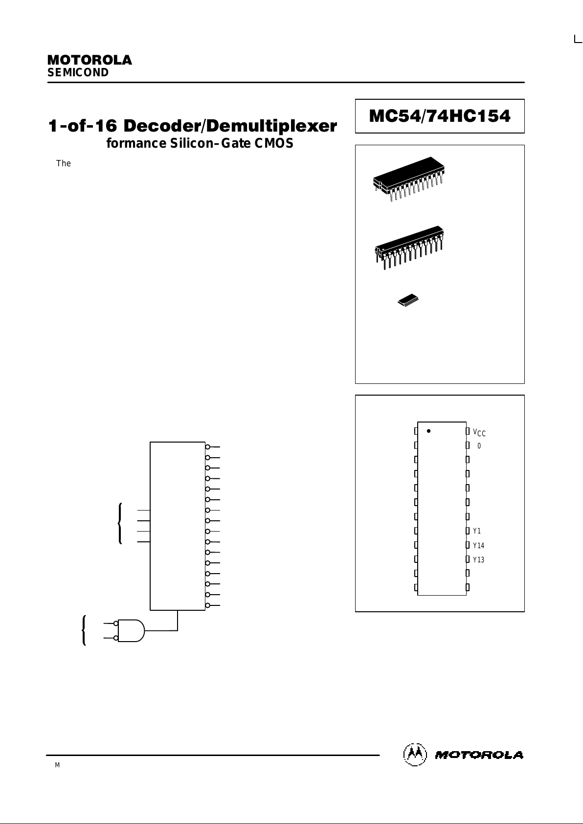
SEMICONDUCTOR TECHNICAL DATA
1
REV 6
Motorola, Inc. 1995
10/95
High–Performance Silicon–Gate CMOS
The MC54/74HC154 is identical in pinout to the LS154. The device inputs
are compatible with standard CMOS outputs; with pullup resistors, they are
compatible with LSTTL outputs.
This device, when enabled, selects one of 16 active–low outputs. Two
active–low Chip Selects are provided to facilitate the chip–select, demultiplexing, a nd cascading f unctions. When either Chip Select is h igh, all
outputs are high. The demultiplexing function is accomplished by using the
Address inputs to select the desired device output. Then, while holding one
chip select input low, data can be applied to the other chip select input (see
Application Note).
The HC154 is primarily used for memory address decoding and data
routing applications.
• Output Drive Capability: 10 LSTTL Loads
• Outputs Directly Interface to CMOS, NMOS, and TTL
• Operating Voltage Range: 2 to 6 V
• Low Input Current: 1 µA
• High Noise Immunity Characteristic of CMOS Devices
• In Compliance with the Requirements Defined by JEDEC Standard
No. 7A
• Chip Complexity: 192 FETs or 48 Equivalent Gates
LOGIC DIAGRAM
Y0
Y1
Y2
Y3
Y4
Y5
Y6
Y7
Y8
Y9
Y10
Y11
Y12
Y13
Y14
Y15
A0
A1
A2
A3
CS1
CS2
18
19
23
22
21
20
1
2
3
4
5
6
7
8
9
10
13
14
15
16
17
BINARY
ADDRESS
INPUTS
CHIP
SELECT
INPUTS
ACTIVE–LOW
OUTPUTS
PIN 24 = V
CC
PIN 12 = GND
11
PIN ASSIGNMENT
Y5
Y3
Y2
Y1
Y0
Y7
Y6
Y4 A3
A2
A1
A0
V
CC
Y13
Y14
Y15
Y11
Y12
CS1
CS2
Y10
GND
Y9
Y8
5
4
3
2
1
10
9
8
7
6
14
15
16
17
18
19
20
13
11
12
21
22
23
24
ORDERING INFORMATION
MC54HCXXXJ
MC74HCXXXN
MC74HCXXXDW
Ceramic
Plastic
SOIC
N SUFFIX
PLASTIC PACKAGE
CASE 724–03
J SUFFIX
CERAMIC PACKAGE
CASE 758–02
DW SUFFIX
SOIC PACKAGE
CASE 751E–04
1
24
1
24
1
24
MC54/74HC154
MOTOROLA High–Speed CMOS Logic Data
DL129 — Rev 6
2
MAXIMUM RATINGS*
Symbol
Parameter
Value
Unit
V
CC
DC Supply Voltage (Referenced to GND)
– 0.5 to + 7.0
V
V
in
DC Input Voltage (Referenced to GND)
– 1.5 to VCC + 1.5
V
V
out
DC Output Voltage (Referenced to GND)
– 0.5 to VCC + 0.5
V
I
in
DC Input Current, per Pin
± 20
mA
I
out
DC Output Current, per Pin
± 25
mA
I
CC
DC Supply Current, VCC and GND Pins
± 50
mA
P
D
Power Dissipation in Still Air,Plastic or Ceramic DIP†
SOIC Package†
750
500
mW
T
stg
Storage Temperature
– 65 to + 150
_
C
T
L
Lead Temperature, 1 mm from Case for 10 Seconds
(Plastic DIP)
(Ceramic DIP or SOIC Package)
260
300
_
C
*Maximum Ratings are those values beyond which damage to the device may occur.
Functional operation should be restricted to the Recommended Operating Conditions.
†Derating — Plastic DIP: – 10 mW/_C from 65_ to 125_C
Ceramic DIP: – 10 mW/_C from 100_ to 125_C
SOIC Package: – 7 mW/_C from 65_ to 125_C
For high frequency or heavy load considerations, see Chapter 2 of the Motorola High–Speed CMOS Data Book (DL129/D).
RECOMMENDED OPERATING CONDITIONS
Symbol
Parameter
Min
Max
Unit
V
CC
DC Supply Voltage (Referenced to GND)
2.0
6.0
V
Vin, V
out
DC Input Voltage, Output Voltage (Referenced to GND)
0
V
CC
V
T
A
Operating Temperature, All Package Types
– 55
+ 125
_
C
tr, t
f
Input Rise and Fall Time VCC = 2.0 V
(Figure 2) VCC = 4.5 V
VCC = 6.0 V
0
0
0
1000
500
400
ns
DC ELECTRICAL CHARACTERISTICS (Voltages Referenced to GND)
Guaranteed Limit
Symbol
Parameter
Test Conditions
V
CC
V
– 55 to
25_C
v
85_Cv 125_C
Unit
V
IH
Minimum High–Level Input
Voltage
V
out
= 0.1 V or VCC – 0.1 V
|I
out
| v 20 µA
2.0
4.5
6.0
1.5
3.15
4.2
1.5
3.15
4.2
1.5
3.15
4.2
V
V
IL
Maximum Low–Level Input
Voltage
V
out
= 0.1 V or VCC – 0.1 V
|I
out
| v 20 µA
2.0
4.5
6.0
0.3
0.9
1.2
0.3
0.9
1.2
0.3
0.9
1.2
V
V
OH
Minimum High–Level Output
Voltage
Vin = VIH or V
IL
|I
out
| v 20 µA
2.0
4.5
6.0
1.9
4.4
5.9
1.9
4.4
5.9
1.9
4.4
5.9
V
Vin = VIH or VIL|I
out
| v 4.0 mA
|I
out
| v 5.2 mA
4.5
6.0
3.98
5.48
3.84
5.34
3.70
5.20
V
OL
Maximum Low–Level Output
Voltage
Vin = VIH or V
IL
|I
out
| v 20 µA
2.0
4.5
6.0
0.1
0.1
0.1
0.1
0.1
0.1
0.1
0.1
0.1
V
Vin = VIH or VIL|I
out
| v 4.0 mA
|I
out
| v 5.2 mA
4.5
6.0
0.26
0.26
0.33
0.33
0.40
0.40
I
in
Maximum Input Leakage Current
Vin = VCC or GND
6.0
± 0.1
± 1.0
± 1.0
µA
I
CC
Maximum Quiescent Supply
Current (per Package)
Vin = VCC or GND
I
out
= 0 µA
6.0
8
80
160
µA
NOTE: Information on typical parametric values can be found in Chapter 2 of the Motorola High–Speed CMOS Data Book (DL129/D).
This device contains protection
circuitry to guard against damage
due to high static voltages or electric
fields. However, precautions must
be taken to avoid applications of any
voltage higher than maximum rated
voltages to this high–impedance circuit. For proper operation, Vin and
V
out
should be constrained to the
range GND v (Vin or V
out
) v VCC.
Unused inputs must always be
tied to an appropriate logic voltage
level (e.g., either GND or VCC).
Unused outputs must be left open.
MC54/74HC154
High–Speed CMOS Logic Data
DL129 — Rev 6
3 MOTOROLA
AC ELECTRICAL CHARACTERISTICS (C
L
= 50 pF, Input tr = tf = 6 ns)
Guaranteed Limit
Symbol
Parameter
V
CC
V
– 55 to
25_C
v
85_Cv 125_C
Unit
t
PLH
,
t
PHL
Maximum Propagation Delay, Input A to Output Y
(Figures 1 and 3)
2.0
4.5
6.0
190
38
32
240
48
41
285
57
48
ns
t
PLH
,
t
PHL
Maximum Propagation Delay, CS to Output Y
(Figures 2 and 3)
2.0
4.5
6.0
175
35
30
220
44
37
265
53
45
ns
t
TLH
,
t
THL
Maximum Output Transition Time, Any Output
(Figures 2 and 3)
2.0
4.5
6.0
75
15
13
95
19
16
110
22
19
ns
C
in
Maximum Input Capacitance
—
10
10
10
pF
NOTES:
1. For propagation delays with loads other than 50 pF, see Chapter 2 of the Motorola High–Speed CMOS Data Book (DL129/D).
2. Information on typical parametric values can be found in Chapter 2 of the Motorola High–Speed CMOS Data Book (DL129/D).
Typical @ 25°C, VCC = 5.0 V
C
PD
Power Dissipation Capacitance (Per Package)*
80
pF
*Used to determine the no–load dynamic power consumption: PD = CPD V
CC
2
f + ICC VCC. For load considerations, see Chapter 2 of the
Motorola High–Speed CMOS Data Book (DL129/D).
PIN DESCRIPTIONS
INPUTS
A0, A1, A2, A3 (Pins 23, 22, 21, 20)
Address inputs. These inputs, when the 1–of–16 decoder
is enabled, determine which of its sixteen active–low outputs
is selected.
OUTPUTS
Y0 – Y15 (Pins 1 – 11, 13 – 17)
Active–low outputs. These outputs assume a low level
when addressed and both chip–select inputs are active.
These outputs remain high when not addressed or a chip–
select input is high.
CONTROL INPUTS
CS1, CS2 (Pins 18, 19)
Active–low chip–select inputs. With low levels on both of
these inputs, the outputs of the decoder follow the Address
inputs. A high level on either input forces all outputs high.
FUNCTION TABLE
Inputs Outputs
CS1 CS2 A3 A2 A1 A0 Y0 Y1 Y2 Y3 Y4 Y5 Y6 Y7 Y8 Y9 Y10 Y11 Y12 Y13 Y14 Y15
L
L
L
L
L
L
L
L
L
L
L
L
L
L
L
L
L
L
L
L
L
L
L
L
L
L
L
L
L
L
L
L
L
L
L
L
L
L
L
L
H
H
H
H
H
H
H
H
L
L
L
L
H
H
H
H
L
L
L
L
H
H
H
H
L
L
H
H
L
L
H
H
L
L
H
H
L
L
H
H
L
H
L
H
L
H
L
H
L
H
L
H
L
H
L
H
L
H
H
H
H
H
H
H
H
H
H
H
H
H
H
H
H
L
H
H
H
H
H
H
H
H
H
H
H
H
H
H
H
H
L
H
H
H
H
H
H
H
H
H
H
H
H
H
H
H
H
L
H
H
H
H
H
H
H
H
H
H
H
H
H
H
H
H
L
H
H
H
H
H
H
H
H
H
H
H
H
H
H
H
H
L
H
H
H
H
H
H
H
H
H
H
H
H
H
H
H
H
L
H
H
H
H
H
H
H
H
H
H
H
H
H
H
H
H
L
H
H
H
H
H
H
H
H
H
H
H
H
H
H
H
H
L
H
H
H
H
H
H
H
H
H
H
H
H
H
H
H
H
L
H
H
H
H
H
H
H
H
H
H
H
H
H
H
H
H
L
H
H
H
H
H
H
H
H
H
H
H
H
H
H
H
H
L
H
H
H
H
H
H
H
H
H
H
H
H
H
H
H
H
L
H
H
H
H
H
H
H
H
H
H
H
H
H
H
H
H
L
H
H
H
H
H
H
H
H
H
H
H
H
H
H
H
H
L
H
H
H
H
H
H
H
H
H
H
H
H
H
H
H
H
L
L
H
H
H
L
H
X
X
X
X
X
X
X
X
X
X
X
X
H
H
H
H
H
H
H
H
H
H
H
H
H
H
H
H
H
H
H
H
H
H
H
H
H
H
H
H
H
H
H
H
H
H
H
H
H
H
H
H
H
H
H
H
H
H
H
H
H = High Level, L = Low Level, X = Don’t Care
 Loading...