

MC34C86MOTOROLA
1
Product Preview
CMOS
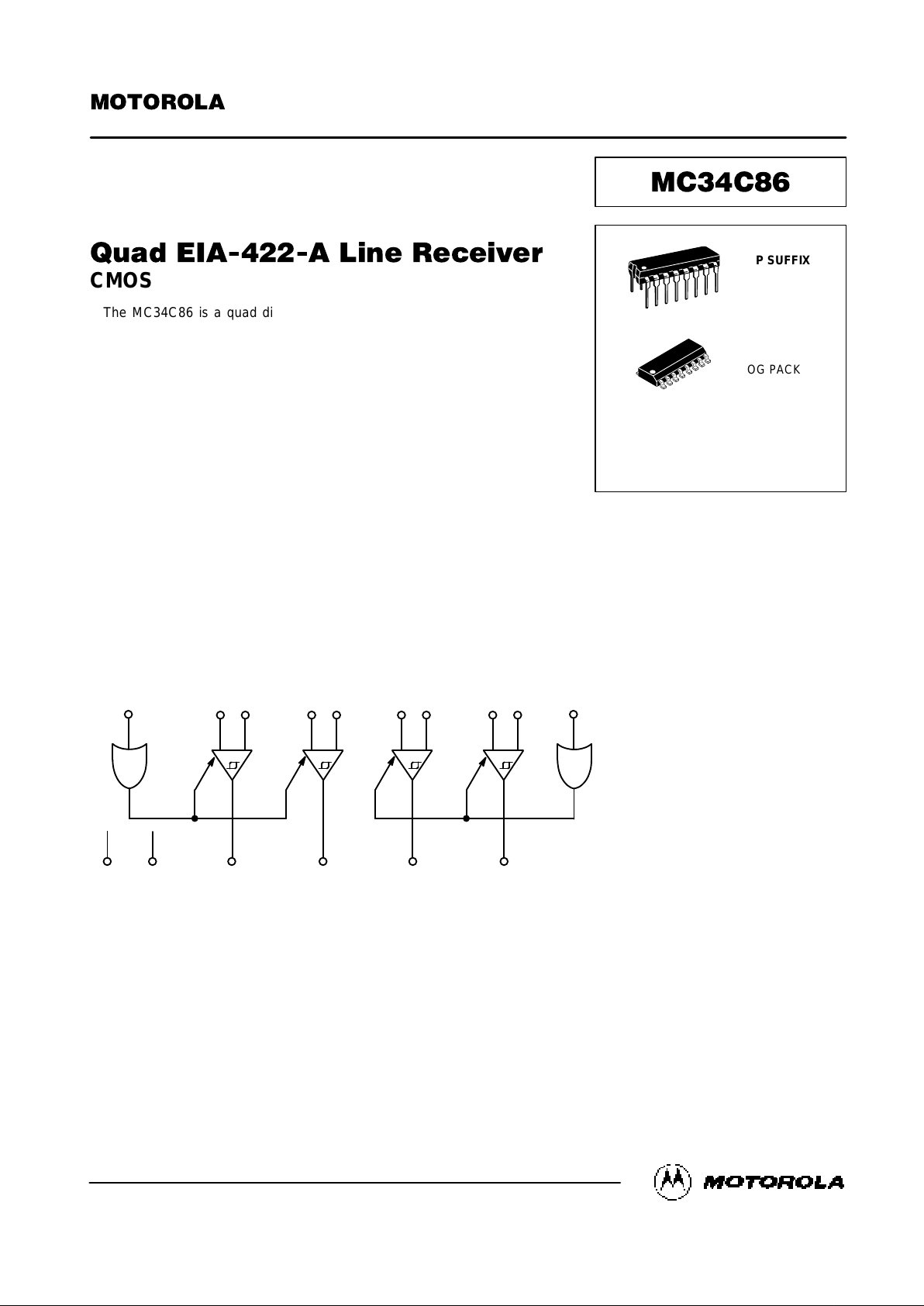
The MC34C86 is a quad differential line receiver designed for digital data
transmission over balanced lines. The MC34C86 meets all the requirements of
standard EIA–422–A while retaining the low–power characteristics of CMOS.
The MC34C86 has an input sensitivity of 200 mV over the common mode
input voltage range of ± 7 V. In addition, each receiver chain has i nternal
hysteresis circuitry to improve noise margin and discourage output instability for
slowly changing input waveforms.
The MC34C86 is pin compatible with the MC3486.
All pins are protected against damage due to electrostatic discharges.
• Typical Power Supply Current: 6 mA
• 2000 V ESD Protection on the Inputs and Outputs
• Typical Propagation Delay: 18 ns
• Typical Input Hysteresis: 75 mV
• Meets the Requirements of Standard EIA–422–A
• Operation from Single 5 V Supply
• High Impedance Mode for Outputs Connected to System Buses
• TTL/CMOS Compatible Outputs
BLOCK DIAGRAM
B/D
CONTROL
INPUT
D2
INPUT
B2
INPUT
C2
INPUT
A2
OUTPUT
D
OUTPUT
B
OUTPUT
C
OUTPUT
A
V
CC
GND
12
10 14 6 2
8 16 11 513 3
+ – + – + – + –
INPUT
D1
9
15 7 1
INPUT
B1
INPUT
C1
INPUT
A1
A/C
CONTROL
4
This document contains information on a product under development. Motorola reserves the right to change or discontinue this product without notice.
Order this document
by MC34C86/D
SEMICONDUCTOR TECHNICAL DATA
P SUFFIX
PLASTIC DIP
CASE 648
D SUFFIX
SOG PACKAGE
CASE 751B
ORDERING INFORMATION
MC34C86P Plastic DIP
MC34C86D SOG Package
16
1
16
1
Motorola, Inc. 1995
REV 4
10/95
MC34C86 MOTOROLA
2
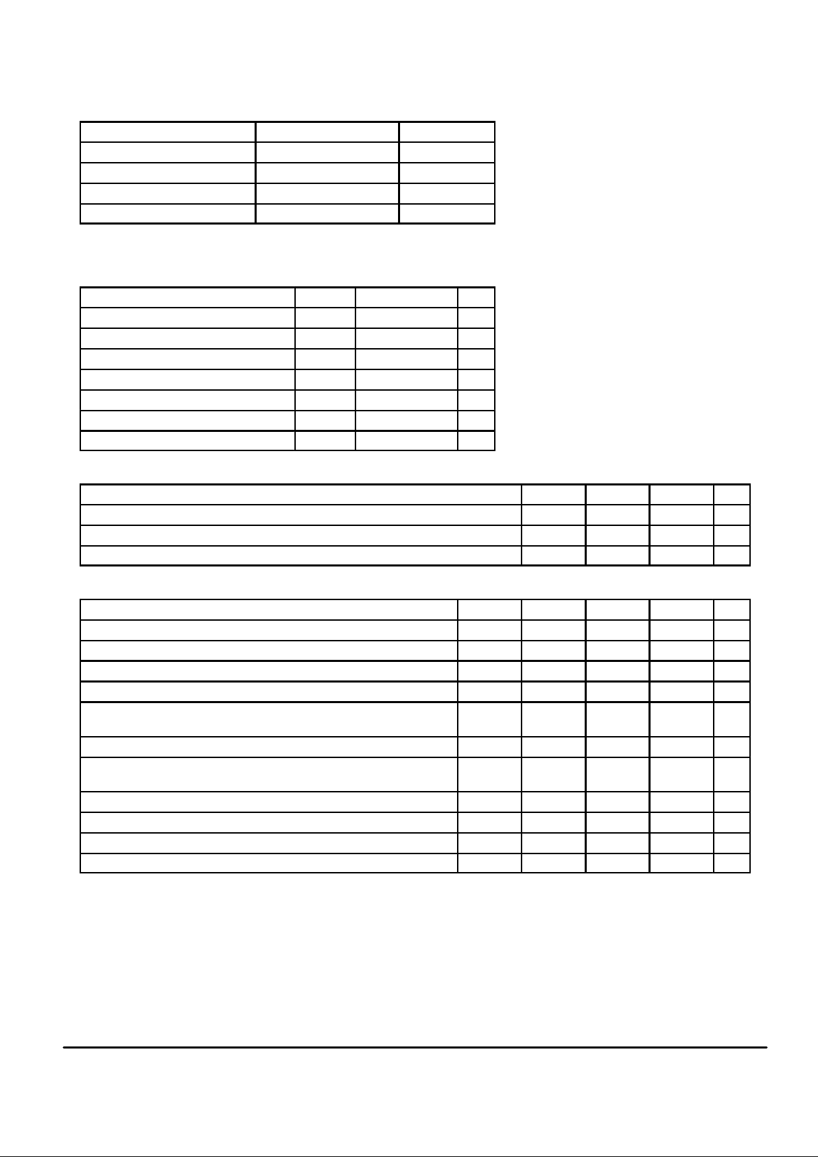
TRUTH TABLE
Control Input Input Output
L X Z
H VID ≥ VTH (Max) 1
H VID ≤ VTH (Min) 0
H Open 1
X = Don’t Care H = High Logic State
Z = High Impedance L = Low Logic State
MAXIMUM RATINGS
Rating Symbol Value Unit
Power Supply Voltage V
CC
7 V
Input Voltage V
I
± 10 V
Input Differential Voltage V
ID
± 14 V
Enable Control Input Voltage V
in
VCC + 0.5 V
Storage Temperature T
stg
– 65 to + 150 °C
Maximum Current per Output I
O
± 25 mA
ESD (Human Body Model) 2000 V
OPERATING CONDITIONS
Rating Symbol Min Max Unit
Power Supply Voltage V
CC
4.5 5.5 V
Operating Temperature Range T
A
– 40 + 85 °C
Input Rise and Fall Time tr, t
f
— 500 ns
DC CHARACTERISTICS (V
CC
= 4.5 to 5.5 V, TA = – 40 to + 85°C, unless otherwise stated) (See Note 1)
Parameter
Symbol Min Typ Max Unit
Power Supply Current, VCC = Max I
CC
— 6 12 mA
Enable Input Current, Vin = VCC or GND I
L
— — ± 1.0 µA
Input Voltage — Low Logic State (Enable Control) V
IL
— — 0.8 V
Input Voltage — High Logic State (Enable Control) V
IH
2 — — V
Differential Input Voltage, – 7 V < V
LCM
< 7 V V
out
= V
OH
V
out
= V
OL
V
TH
0.2
—
—
—
—
– 0.2
V
Input Hysteresis, V
LCM
= 0 V V
hys
— 75 — mV
Comparator Input Current Vin = + 10 V, Other Input = GND
Vin = – 10 V, Other Input = GND
I
in
—
—
1.4
– 2.5
—
—
mA
Comparator Input Resistance, – 10 V < V
LCM
< + 10 V R
in
4 4.8 — kΩ
Output Voltage (Low Logic State) VID = – 1 V, I
out
= 6 mA (Note 2) V
OL
— 0.13 0.33 V
Output Voltage (High Logic State) VID = + 1 V, I
out
= – 6 mA (Note 2) V
OH
3.8 4.8 — V
Output Leakage Current (High Logic State) V
out
= VCC or GND I
OZ
– 5 — 5 µA
NOTES:
1. All currents into device pins are shown as positive, out of device pins are negative. All voltages referenced to ground unless otherwise noted.
2. See EIA specifications EIA–422–A for exact test conditions.
This device contains circuitry to protect the
inputs against damage due to high static voltages or electric fields; however, it is advised that
normal precautions be taken to avoid applications of any voltage higher than the maximum
rated voltages to this high impedance circuit.
For proper operation it is recommended that
Vin and V
out
be constrained to the range VSS ≤
(Vin or V
out
) ≤ VDD. Reliability of operation is
enhanced if unused inputs are tied to and
appropriate logic voltage level (e.g., either V
SS
or VDD).

MC34C86MOTOROLA
3
AC CHARACTERISTICS (V
CC
= 4.5 to 5.5 V, TA = – 40 to + 85°C, unless otherwise stated)
Parameter
Symbol Min Typ Max Unit
Propagation Delay Input to Output, CL = 50 pF, V
DIFF
= 2.5 V t
PLH
t
PHL
— 18 30 ns
Skew = t
PHL
– t
PLH
Skew — 1 — ns
Propagation Delay Enable to Output
CL = 50 pF, RL = 1000 Ω, V
DIFF
= 2.5 V
t
PLZ
t
PHZ
— 12 — ns
Propagation Delay Enable to Output
CL = 50 pF, RL = 1000 Ω, V
DIFF
= 2.5 V
t
PZL
t
PZH
— 14 — ns
AC TEST CIRCUIT AND SWITCHING TIME WAVEFORMS
Figure 1. Test Circuit
4.9 k
Ω
S1
V
CC
OUTPUT
S2
CL = 49 pF
RL = 2 k
Ω
TEST
POINT
OUTPUT
0 V
t
PHL
Figure 2. Propagation Delays
1.3 V 1.3 V
0 V
INPUT
t
PLH
+ 2.5 V —
– 2.5 V
S1 AND S2 CLOSED
Figure 3. Enable and Disable Times
OUTPUT A
1.3 V
t
PHZ
OUTPUT B
50%
1.3 VENABLE INPUT
50%
V
OL
V
OH
t
PZH
t
PLZ
t
PZL
3 V —
0 V
S1 OPEN
S2 CLOSED
S1 CLOSED
S2 CLOSED
S1 CLOSED
S2 OPEN
S1 CLOSED
S2 CLOSED
0.5 V
0.5 V
TYPICAL APPLICATIONS
Figure 4. Two–Wire Balanced Systems (EIA–422–A)
+
–
DATA
DATA
OUTPUT
ENABLE

MC34C86 MOTOROLA
4
PACKAGE DIMENSIONS
P SUFFIX
PLASTIC DIP
CASE 648–08
NOTES:
1. DIMENSIONING AND TOLERANCING PER ANSI
Y14.5M, 1982.
2. CONTROLLING DIMENSION: INCH.
3. DIMENSION L TO CENTER OF LEADS WHEN
FORMED PARALLEL.
4. DIMENSION B DOES NOT INCLUDE MOLD FLASH.
5. ROUNDED CORNERS OPTIONAL.
–A–
B
F
C
S
H
G
D
J
L
M
16 PL
SEATING
1 8
916
K
PLANE
–T–
M
A
M
0.25 (0.010) T
DIM MIN MAX MIN MAX
MILLIMETERSINCHES
A 0.740 0.770 18.80 19.55
B 0.250 0.270 6.35 6.85
C 0.145 0.175 3.69 4.44
D 0.015 0.021 0.39 0.53
F 0.040 0.70 1.02 1.77
G 0.100 BSC 2.54 BSC
H 0.050 BSC 1.27 BSC
J 0.008 0.015 0.21 0.38
K 0.110 0.130 2.80 3.30
L 0.295 0.305 7.50 7.74
M 0 10 0 10
S 0.020 0.040 0.51 1.01
____
D SUFFIX
SOG PACKAGE
CASE 751B–05
NOTES:
1. DIMENSIONING AND TOLERANCING PER ANSI
Y14.5M, 1982.
2. CONTROLLING DIMENSION: MILLIMETER.
3. DIMENSIONS A AND B DO NOT INCLUDE
MOLD PROTRUSION.
4. MAXIMUM MOLD PROTRUSION 0.15 (0.006)
PER SIDE.
5. DIMENSION D DOES NOT INCLUDE DAMBAR
PROTRUSION. ALLOWABLE DAMBAR
PROTRUSION SHALL BE 0.127 (0.005) TOTAL
IN EXCESS OF THE D DIMENSION AT
MAXIMUM MATERIAL CONDITION.
1 8
16 9
SEATING
PLANE
F
J
M
R
X 45
_
G
8 PLP
–B–
–A–
M
0.25 (0.010) B
S
–T–
D
K
C
16 PL
S
B
M
0.25 (0.010) A
S
T
DIM MIN MAX MIN MAX
INCHESMILLIMETERS
A 9.80 10.00 0.386 0.393
B 3.80 4.00 0.150 0.157
C 1.35 1.75 0.054 0.068
D 0.35 0.49 0.014 0.019
F 0.40 1.25 0.016 0.049
G 1.27 BSC 0.050 BSC
J 0.19 0.25 0.008 0.009
K 0.10 0.25 0.004 0.009
M 0 7 0 7
P 5.80 6.20 0.229 0.244
R 0.25 0.50 0.010 0.019
_ _ _ _
Motorola reserves the right to make changes without further notice to any products herein. Motorola makes no warranty, representation or guarantee regarding
the suitability of its products for any particular purpose, nor does Motorola assume any liability arising out of the application or use of any product or circuit,
and specifically disclaims any and all liability, including without limitation consequential or incidental damages. “T ypical” parameters can and do vary in different
applications. All operating parameters, including “T ypicals” must be validated for each customer application by customer’s technical experts. Motorola does
not convey any license under its patent rights nor the rights of others. Motorola products are not designed, intended, or authorized for use as components in
systems intended for surgical implant into the body, or other applications intended to support or sustain life, or for any other application in which the failure of
the Motorola product could create a situation where personal injury or death may occur. Should Buyer purchase or use Motorola products for any such
unintended or unauthorized application, Buyer shall indemnify and hold Motorola and its officers, employees, subsidiaries, affiliates, and distributors harmless
against all claims, costs, damages, and expenses, and reasonable attorney fees arising out of, directly or indirectly, any claim of personal injury or death
associated with such unintended or unauthorized use, even if such claim alleges that Motorola was negligent regarding the design or manufacture of the part.
Motorola and are registered trademarks of Motorola, Inc. Motorola, Inc. is an Equal Opportunity/Affirmative Action Employer.
How to reach us:
USA/EUROPE: Motorola Literature Distribution; JAPAN: Nippon Motorola Ltd.; Tatsumi–SPD–JLDC, Toshikatsu Otsuki,
P.O. Box 20912; Phoenix, Arizona 85036. 1–800–441–2447 6F Seibu–Butsuryu–Center, 3–14–2 Tatsumi Koto–Ku, Tokyo 135, Japan. 03–3521–8315
MFAX: RMFAX0@email.sps.mot.com – TOUCHTONE (602) 244–6609 HONG KONG: Motorola Semiconductors H.K. Ltd.; 8B Tai Ping Industrial Park,
INTERNET: http://Design–NET.com 51 Ting Kok Road, Tai Po, N.T., Hong Kong. 852–26629298
MC34C86/D
*MC34C86/D*
◊
 Loading...