

Motorola MC34262D, MC34262P, MC33262D, MC33262P Datasheet
The MC34262/MC33262 are active power factor controllers specifically
designed for use as a preconverter in electronic ballast and in off–line power
converter applications. These integrated circuits feature an internal startup
timer for stand–alone applications, a one quadrant multiplier for near unity
power factor, zero current detector to ensure critical conduction operation,
transconductance error amplifier, quickstart circuit for enhanced startup,
trimmed internal bandgap reference, current sensing comparator, and a
totem pole output ideally suited for driving a power MOSFET.
Also included are protective features consisting of an overvoltage
comparator to eliminate runaway output voltage due to load removal, input
undervoltage lockout with hysteresis, cycle–by–cycle current limiting,
multiplier output clamp that limits maximum peak switch current, an RS latch
for single pulse metering, and a drive output high state clamp for MOSFET
gate protection. These devices are available in dual–in–line and surface
mount plastic packages.
• Overvoltage Comparator Eliminates Runaway Output Voltage
• Internal Startup Timer
• One Quadrant Multiplier
• Zero Current Detector
• Trimmed 2% Internal Bandgap Reference
• Totem Pole Output with High State Clamp
• Undervoltage Lockout with 6.0 V of Hysteresis
• Low Startup and Operating Current
• Supersedes Functionality of SG3561 and TDA4817
Order this document by MC34262/D
POWER FACTOR
CONTROLLERS
SEMICONDUCTOR
TECHNICAL DATA
PLASTIC PACKAGE
8
1
8
1
PLASTIC PACKAGE
P SUFFIX
CASE 626
D SUFFIX
CASE 751
(SO–8)
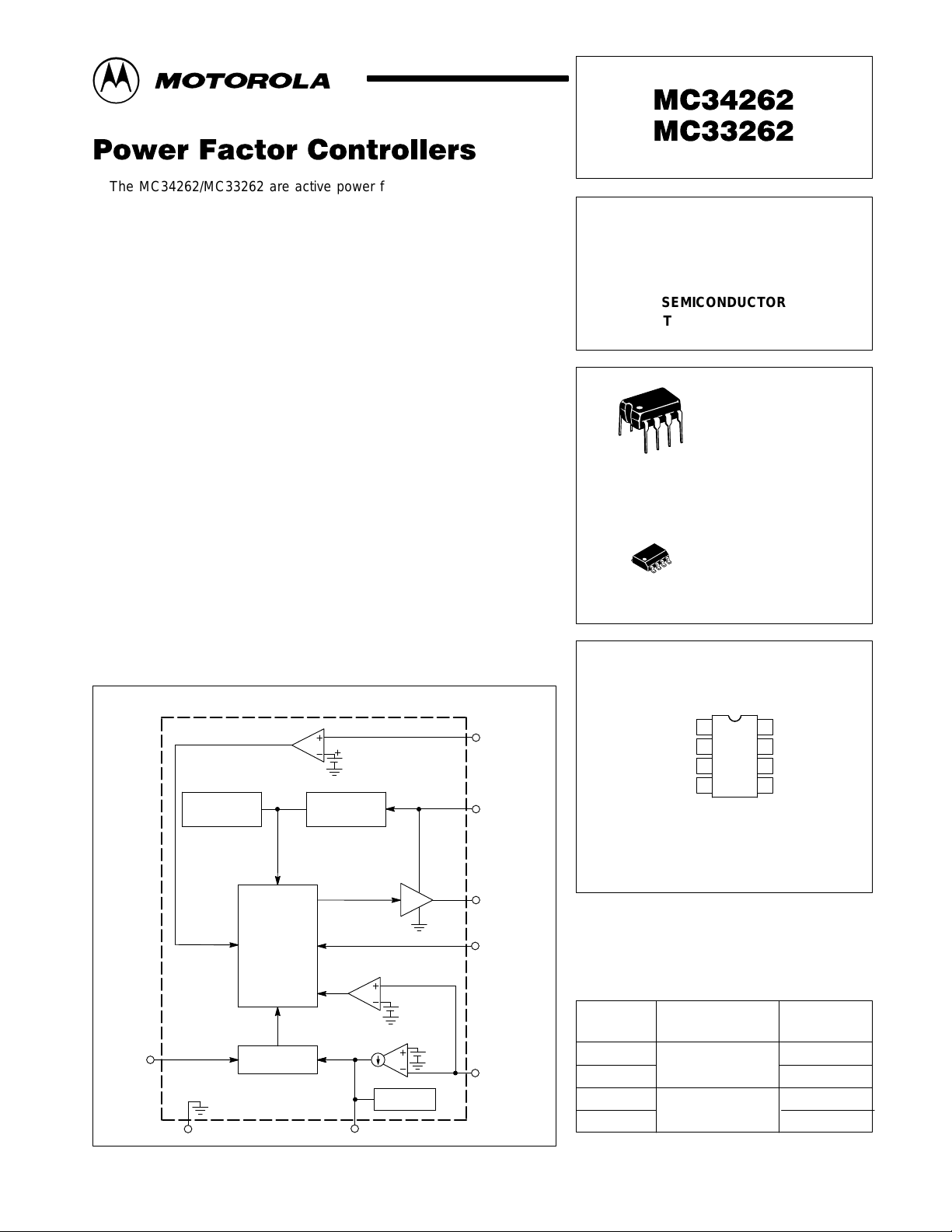
Multiplier
Input
PIN CONNECTIONS
Simplified Block Diagram
Zero Current Detector
2.5V
Reference
Multiplier,
Latch,
PWM,
Timer,
Logic
3
6
Gnd
Multiplier
Undervoltage
Lockout
&
Compensation
Error Amp
2
Overvoltage
Comparator
+
1.08 V
+
Quickstart
ref
V
ref
Zero Current
Detect Input
5
V
CC
8
Drive Output
7
Current Sense
Input
4
Voltage
Feedback
1
Input
Voltage Feedback
Compensation
Multiplier Input
Current Sense
ORDERING INFORMATION
Device
MC34262D
MC34262P
MC33262D
MC33262P
1
Input
2
3
4
Input
(Top View)
Operating
Temperature Range
TA = 0° to +85°C
TA = –40° to +105°C
V
8
CC
7
Drive Output
Gnd
6
Zero Current
5
Detect Input
Package
Plastic DIP
Plastic DIP
SO–8
SO–8
MOTOROLA ANALOG IC DEVICE DATA
Motorola, Inc. 1996 Rev 1
1
MC34262 MC33262
MAXIMUM RATINGS
Rating Symbol Value Unit
Total Power Supply and Zener Current (ICC + IZ) 30 mA
Output Current, Source or Sink (Note 1) I
Current Sense, Multiplier, and V oltage Feedback Inputs V
Zero Current Detect Input
High State Forward Current
Low State Reverse Current
Power Dissipation and Thermal Characteristics
P Suffix, Plastic Package, Case 626
Maximum Power Dissipation @ TA = 70°C
Thermal Resistance, Junction–to–Air
D Suffix, Plastic Package, Case 751
Maximum Power Dissipation @ TA = 70°C
Thermal Resistance, Junction–to–Air
Operating Junction Temperature T
Operating Ambient Temperature (Note 3)
MC34262
MC33262
Storage Temperature T
R
R
O
I
in
P
θJA
P
θJA
T
stg
in
D
D
J
A
500 mA
–1.0 to +10 V
50
–10
800
100
450
178
+150 °C
0 to + 85
– 40 to +105
– 65 to +150 °C
mA
mW
°C/W
mW
°C/W
°C
ELECTRICAL CHARACTERISTICS (V
temperature range that applies [Note 3], unless otherwise noted.)
Characteristic
ERROR AMPLIFIER
Voltage Feedback Input Threshold
TA = 25°C
TA = T
Line Regulation (VCC = 12 V to 28 V, TA = 25°C) Reg
Input Bias Current (VFB = 0 V) I
Transconductance (TA = 25°C) g
Output Current
Source (VFB = 2.3 V)
Sink (VFB = 2.7 V)
Output Voltage Swing
High State (VFB = 2.3 V)
Low State (VFB = 2.7 V)
OVERVOLTAGE COMPARATOR
Voltage Feedback Input Threshold V
MULTIPLIER
Input Bias Current, Pin 3 (VFB = 0 V) I
Input Threshold, Pin 2 V
Dynamic Input Voltage Range
Multiplier Input (Pin 3)
Compensation (Pin 2)
Multiplier Gain (V
ZERO CURRENT DETECTOR
Input Threshold Voltage (Vin Increasing) V
Hysteresis (Vin Decreasing) V
Input Clamp Voltage
High State (I
Low State (I
low
to T
DET
DET
(VCC = 12 V to 28 V)
high
= 0.5 V, V
Pin 3
= + 3.0 mA)
= – 3.0 mA)
Pin 2
= 12 V (Note 2), for typical values TA = 25°C, for min/max values TA is the operating ambient
CC
V
V
= V
+ 1.0 V) (Note 4) K 0.43 0.65 0.87 1/V
th(M)
Symbol Min Typ Max Unit
V
FB
line
IB
m
I
O
OH(ea)
OL(ea)
FB(OV)
IB
th(M)
V
Pin 3
V
Pin 2
th
H
V
IH
V
IL
2.465
2.44
— 1.0 10 mV
— –0.1 – 0.5 µA
80 100 130 µmho
—
—
5.8
—
1.065 V
FB
— –0.1 – 0.5 µA
1.05 V
OL(EA)
0 to 2.5
V
to
th(M)
(V
+ 1.0)
th(M)
1.33 1.6 1.87 V
100 200 300 mV
6.1
0.3
1.08 V
1.2 V
V
(V
th(M)
2.5
—
10
10
6.4
1.7
OL(EA)
0 to 3.5
th(M)
+ 1.5)
6.7
0.7
FB
to
2.535
2.54
—
—
—
2.4
1.095 V
— V
—
—
—
1.0
FB
V
µA
V
V
V
V
2
MOTOROLA ANALOG IC DEVICE DATA
MC34262 MC33262
.
ELECTRICAL CHARACTERISTICS (V
= 12 V (Note 2), for typical values TA = 25°C, for min/max values TA is the operating ambient
CC
temperature range that applies (Note 3), unless otherwise noted.)
Characteristic
CURRENT SENSE COMPARATOR
Input Bias Current (V
Input Offset Voltage (V
= 0 V) I
Pin 4
Pin 2
= 1.1 V, V
= 0 V) V
Pin 3
Maximum Current Sense Input Threshold (Note 5) V
Delay to Output t
DRIVE OUTPUT
Output Voltage (VCC = 12 V)
Low State (I
Low State (I
High State (I
High State (I
= 20 mA)
Sink
= 200 mA)
Sink
Source
Source
= 20 mA)
= 200 mA)
Output Voltage (VCC = 30 V)
High State (I
= 20 mA, CL = 15 pF)
Source
Output Voltage Rise T ime (CL = 1.0 nF) t
Output Voltage Fall T ime (CL = 1.0 nF) t
Output Voltage with UVLO Activated
(VCC = 7.0 V, I
Sink
= 1.0 mA)
RESTART TIMER
Restart Time Delay t
UNDERVOLTAGE LOCKOUT
Startup Threshold (VCC Increasing) V
Minimum Operating Voltage After Turn–On (VCC Decreasing) V
Hysteresis V
TOTAL DEVICE
Power Supply Current
Startup (VCC = 7.0 V)
Operating
Dynamic Operating (50 kHz, CL = 1.0 nF)
Power Supply Zener Voltage (ICC = 25 mA) V
NOTES: 1. Maximum package power dissipation limits must be observed.
2.Adjust VCC above the startup threshold before setting to 12 V.
3. T
=0°C for MC34262
low
3. T
=–40°C for MC33262
low
T
=+85°C for MC34262
high
T
= +105°C for MC33262
high
Symbol Min Typ Max Unit
IB
IO
th(max)
PHL(in/out)
V
OL
V
OH
V
O(max)
r
f
V
O(UVLO)
DLY
th(on)
Shutdown
H
I
CC
Z
— – 0.15 –1.0 µA
— 9.0 25 mV
1.3 1.5 1.8 V
— 200 400 ns
—
—
9.8
7.8
0.3
2.4
10.3
8.4
0.8
3.3
—
—
14 16 18
— 50 120 ns
— 50 120 ns
— 0.1 0.5 V
200 620 — µs
11.5 13 14.5 V
7.0 8.0 9.0 V
3.8 5.0 6.2 V
—
—
—
0.25
6.5
9.0
0.4
12
20
30 36 — V
4. K =
5.This parameter is measured with VFB = 0 V, and V
Pin 4 Threshold
V
(V
Pin 3
Pin 2
– V
th(M)
)
Pin 3
V
V
mA
= 3.0 V
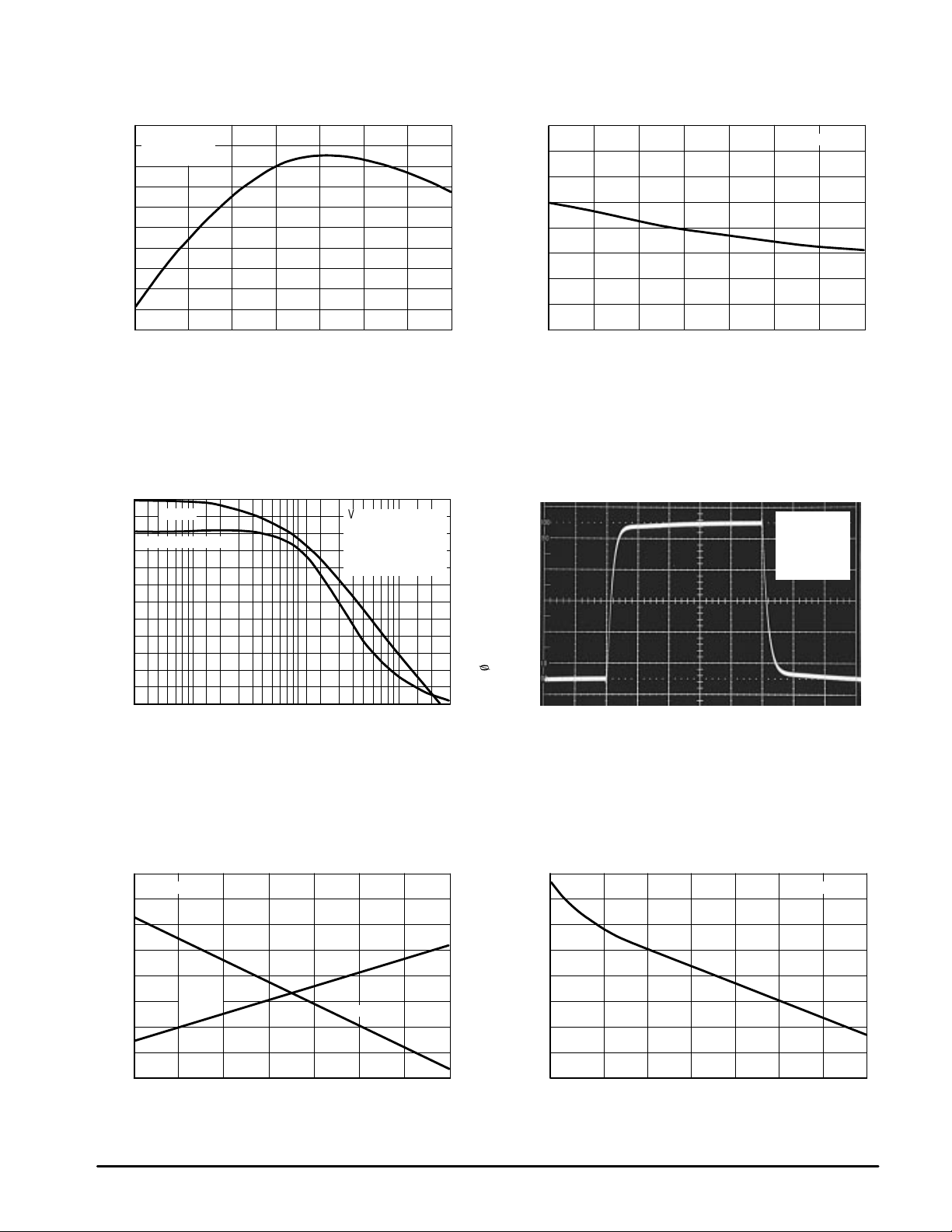
Figure 1. Current Sense Input Threshold
versus Multiplier Input
1.6
VCC = 12 V
1.4
TA = 25
°
C
1.2
1.0
0.8
0.6
0.4
0.2
, CURRENT SENSE PIN 4 THRESHOLD (V)
0
CS
V
1.4– 0.2 3.80.6 2.2 3.0
VM, MULTIPLIER PIN 3 INPUT VOLTAGE (V)
MOTOROLA ANALOG IC DEVICE DATA
V
Pin 2
= 2.0 V
, CURRENT SENSE PIN 4 THRESHOLD (V)
V
CS
0.08
0.07
0.06
0.05
0.04
0.03
0.02
0.01
– 0.12
Figure 2. Current Sense Input Threshold
versus Multiplier Input, Expanded View
V
= 3.5 V
Pin 2
V
= 3.25 V
Pin 2
0
– 0.06 0.06 0.12 0.18 0.240
VM, MULTIPLIER PIN 3 INPUT VOLTAGE (V)
VCC = 12 V
TA = 25
V
Pin 2
°
C
= 2.0 V
3
MC34262 MC33262
Figure 3. V oltage Feedback Input Threshold
Change versus T emperature
4.0
VCC = 12 V
Pins 1 to 2
0
– 4.0
– 8.0
–12
, VOLTAGE FEEDBACK THRESHOLD CHANGE (mV)
–16
FB
–55
V
∆
– 25 0 25 50 75 100 125
TA, AMBIENT TEMPERATURE (
Figure 5. Error Amp Transconductance and
Phase versus Frequency
120
100
µ
Phase
Transconductance
80
°
C)
VCC = 12 V
VO = 2.5 V to 3.5 V
RL = 100 k to 3.0 V
CL = 2.0 pF
°
C
TA = 25
0
30
60
Figure 4. Overvoltage Comparator Input
FB
110
109
108
107
, OVERVOLTAGE INPUT THRESHOLD (%V )
106
–55
FB(OV)
V
Threshold versus T emperature
– 25 0 25 50 75 100
Figure 6. Error Amp Transient Response
4.00 V
TA, AMBIENT TEMPERATURE (
VCC = 12 V
°
C)
VCC = 12 V
RL = 100 k
CL = 2.0 pF
TA = 25
125
°
C
60
40
20
, TRANSCONDUCTANCE ( mho)
m
g
0
3.0 k 10 k 30 k 100 k 300 k 1.0 M 3.0 M
f, FREQUENCY (Hz)
Figure 7. Quickstart Charge Current
versus T emperature
1.80
VCC = 12 V
1.76
1.72
Voltage
1.68
, QUICKSTAR T CHARGE VOLTAGE (V)
chg
V
1.64
– 55 – 25 0 25 50 75 100 125
TA, AMBIENT TEMPERATURE (°C)
Current
90
120
150
180
900
800
700
600
500
3.25 V
, EXCESS PHASE (DEGREES)
O
2.50 V
800
µ
µ
700
600
, RESTART TIME DELAY ( s)
500
DLY
t
, QUICKSTART CHARGE CURRENT ( A)
chg
I
400
–55
5.0 µs/DIV
Figure 8. Restart Timer Delay
versus T emperature
VCC = 12 V
– 25 0 25 50 75 100 125
TA, AMBIENT TEMPERATURE (
°
C)
0.75 V/DIV
4
MOTOROLA ANALOG IC DEVICE DATA
MC34262 MC33262
1.7
1.6
1.5
, THRESHOLD VOLTAGE (V)
1.4
th
V
1.3
90%
Figure 9. Zero Current Detector Input
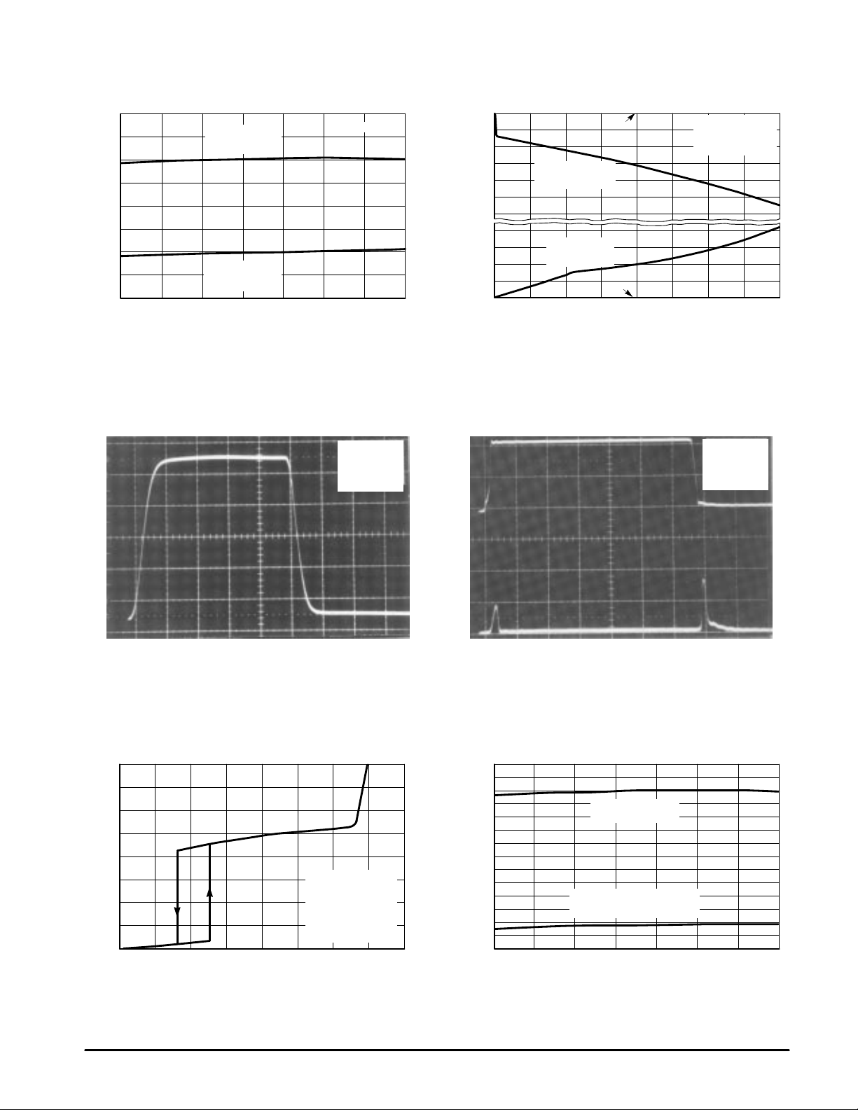
Threshold V oltage versus Temperature
Upper Threshold
(Vin, Increasing)
Lower Threshold
(Vin, Decreasing)
– 25 0 25 50 75 100 125
–55
TA, AMBIENT TEMPERATURE (
°
Figure 11. Drive Output Waveform
VCC = 12 V
C)
VCC = 12 V
CL = 1.0 nF
TA = 25
Figure 10. Output Saturation Voltage
versus Load Current
0
– 2.0
– 4.0
– 6.0
4.0
2.0
, OUTPUT SA TURATION VOLTAGE (V)
sat
V
0
0 80 160 240 320
Source Saturation
(Load to Ground)
Sink Saturation
(Load to VCC)
V
CC
Gnd
IO, OUTPUT LOAD CURRENT (mA)
VCC = 12 V
µ
s Pulsed Load
80
120 Hz Rate
Figure 12. Drive Output Cross Conduction
VCC = 12 V
CL = 15 pF
°
C
°
C
, OUTPUT VOL TAGE
O
TA = 25
5.0 V/DIV100 mA/DIV
10%
100 ns/DIV 100 ns/DIV
Figure 13. Supply Current
versus Supply V oltage
16
12
8.0
VFB = 0 V
, SUPPLY CURRENT (mA)
4.0
CC
I
0
0 10203040
V
, SUPPLY VOLTAGE (V)
CC
Current Sense = 0 V
Multiplier = 0 V
CL = 1.0 nF
f = 50 kHz
°
C
TA = 25
, SUPPLY CURRENT V
CC
I
Figure 14. Undervoltage Lockout Thresholds
versus T emperature
14
13
12
11
10
, SUPPLY VOLTAGE (V)
9.0
CC
V
8.0
7.0
– 55 – 25 0 25 50 75 100 125
Startup Threshold
(VCC Increasing)
Minimum Operating Threshold
(VCC Decreasing)
TA, AMBIENT TEMPERATURE (°C)
MOTOROLA ANALOG IC DEVICE DATA
5
 Loading...