

MOTOROLA MC34261DR2, MC33261P, MC33261D, MC33261DR2 Datasheet
SEMICONDUCTOR
TECHNICAL DATA
POWER FACTOR
CONTROLLERS
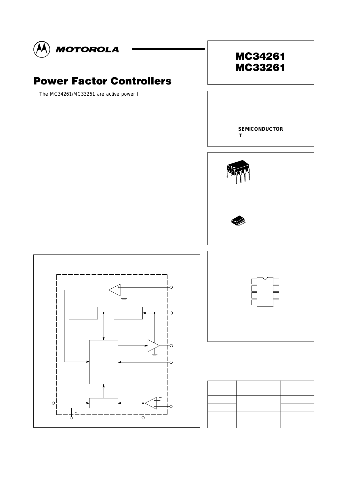
PIN CONNECTIONS
Order this document by MC34261/D
D SUFFIX
PLASTIC PACKAGE
CASE 751
(SO–8)
8
1
8
1
P SUFFIX
PLASTIC PACKAGE
CASE 626
Voltage Feedback
Input
1
2
3
4
8
7
6
5
(Top View)
Compensation
Multiplier Input
Current Sense
Input
V
CC
Drive Output
Gnd
Zero Current
Detect Input
Device
Operating
Temperature Range
Package
ORDERING INFORMATION
MC34261D
MC34261P
TA = 0° to +70°C
SO–8
Plastic DIP
MC33261D
MC33261P
SO–8
Plastic DIP
TA = –40° to +85°C
1
MOTOROLA ANALOG IC DEVICE DATA
The MC34261/MC33261 are active power factor controllers specifically
designed for use as a preconverter in electronic ballast and in off–line power
converter applications. These integrated circuits feature an internal startup
timer, a one quadrant multiplier for near unity power factor, zero current
detector to ensure critical conduction operation, high gain error amplifier,
trimmed internal bandgap reference, current sensing comparator, and a
totem pole output ideally suited for driving a power MOSFET.
Also included are protective features consisting of input undervoltage
lockout with hysteresis, cycle–by–cycle current limiting, and a latch for single
pulse metering. These devices are available in dual–in–line and surface
mount plastic packages.
• Internal Startup Timer
• One Quadrant Multiplier
• Zero Current Detector
• Trimmed 2% Internal Bandgap Reference
• Totem Pole Output
• Undervoltage Lockout with Hysteresis
• Low Startup and Operating Current
• Pinout Equivalent to the SG3561
• Functional Equivalent to the TDA4817
Simplified Block Diagram
Voltage
Feedback
Input
Multiplier,
Latch,
PWM,
Timer,
&
Logic
V
ref
Error Amp
Multiplier
Undervoltage
Lockout
2.5V
Reference
Zero Current Detector
5
8
6
7
4
3
2
1
Drive Output
Gnd
Zero Current
Detect Input
Multiplier
Input
Compensation
V
CC
Current Sense
Input
Motorola, Inc. 1996 Rev 1
MC34261 MC33261
2
MOTOROLA ANALOG IC DEVICE DATA
MAXIMUM RATINGS
Rating Symbol Value Unit
Total Power Supply and Zener Current (ICC + IZ) 30 mA
Output Current, Source or Sink (Note 1) I
O
500 mA
Current Sense, Multiplier, and Voltage Feedback Inputs V
in
–1.0 to 10 V
Zero Current Detect Input
High State Forward Current
Low State Reverse Current
I
in
50
–10
mA
Power Dissipation and Thermal Characteristics
P Suffix, Plastic Package Case 626
Maximum Power Dissipation @ TA = 70°C
Thermal Resistance, Junction–to–Air
D Suffix, Plastic Package Case 626
Maximum Power Dissipation @ TA = 70°C
Thermal Resistance, Junction–to–Air
P
D
R
θJA
P
D
R
θJA
800
100
450
178
mW
°C/W
mW
°C/W
Operating Junction Temperature T
J
+150 °C
Operating Ambient Temperature (Note 3)
MC34261
MC33261
T
A
0 to +70
–40 to +85
°C
Storage Temperature T
stg
–55 to +150 °C
ELECTRICAL CHARACTERISTICS (V
CC
= 12 V, for typical values TA = 25°C, for min/max values TA is the operating ambient
temperature range that applies [Note 3], unless otherwise noted.)
Characteristic
Symbol Min Typ Max Unit
ERROR AMPLIFIER
Voltage Feedback Input Threshold
TA = 25°C
TA = T
low
to T
high
(VCC = 12 V to 28 V)
V
FB
2.465
2.44
2.5 2.535
2.54
V
Line Regulation (VCC = 12 V to 28 V, TA = 25°C) Reg
line
– 1.0 10 mV
Input Bias Current (VFB = 0 V) I
IB
– –0.3 –1.0 µA
Open Loop Voltage Gain A
VOL
65 85 – dB
Gain Bandwidth Product (TA = 25°C) GBW 0.7 1.0 – MHz
Output Source Current (VO = 4.0 V , VFB = 2.3 V) I
Source
0.25 0.5 0.75 mA
Output Voltage Swing
High State (I
Source
= 0.2 mA, VFB = 2.3 V)
Low State (I
Sink
= 0.4 mA, VFB = 2.7 V)
V
OH
V
OL
5.0
–
5.7
2.1
–
2.44
V
MULTIPLIER
Dynamic Input Voltage Range
Multiplier Input (Pin 3)
Compensation (Pin 2)
V
Pin 3
V
Pin 2
0 to 2.5
VFB to
(VFB + 1.0)
0 to 3.5
VFB to
(VFB + 1.5)
–
–
V
Input Bias Current (VFB = 0 V) I
IB
– –0.3 –1.0 µA
Multiplier Gain (V
Pin 3
= 0.5 V , V
Pin 2
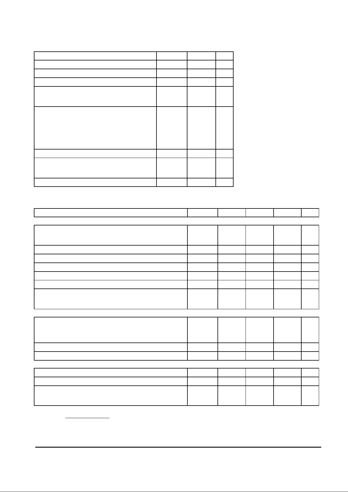
= VFB + 1.0 V) (Note 2) K 0.4 0.62 0.8 1/V
ZERO CURRENT DETECTOR
Input Threshold Voltage (Vin Increasing) V
th
1.3 1.6 1.8 V
Hysteresis (Vin Decreasing) V
H
40 110 200 mV
Input Clamp Voltage
High State (I
DET
= 3.0 mA)
Low State (I
DET
= –3.0 mA)
V
IH
V
IL
6.1
0.3
6.7
0.7
–
1.0
V
NOTES: 1. Maximum package power dissipation limits must be observed.
3. T
low
= –40°C for MC34261
3. T
low
= –40°C for MC33261
T
high
= +70°C for MC34261
T
high
= +85°C for MC33261
Pin 4 Threshold Voltage
V
Pin 3(VPin 2
– VFB)
2. K =
MC34261 MC33261
3
MOTOROLA ANALOG IC DEVICE DATA
ELECTRICAL CHARACTERISTICS (V
CC
= 12 V, for typical values TA = 25°C, for min/max values TA is the operating ambient
temperature range that applies [Note 3], unless otherwise noted.)
Characteristic
Symbol Min Typ Max Unit
CURRENT SENSE COMPARATOR
Input Bias Current (V
Pin 4
= 0 V) I
IB
– –0.5 –2.0 µA
Input Offset Voltage (V
Pin 2
= 1.1 V , V
Pin 3
= 0 V) V
IO
– 3.5 15 mV
Delay to Output t
PHL (in/out)
– 200 400 ns
DRIVE OUTPUT
Output Voltage (VCC = 12 V)
Low State (I
Sink
= 20 mA)
Low State (I
Sink
= 200 mA)
High State (I
Source
= 20 mA)
High State (I
Source
= 200 mA)
V
OL
V
OH
–
1.8
9.8
7.8
0.3
2.4
10.3
8.3
0.8
3.3
–
8.8
V
Output Voltage (VCC = 30 V)
High State (I
Source
= 20 mA, CL = 15 pF)
V
O(max)
14 16 18
V
Output Voltage Rise T ime (CL = 1.0 nF) t
r
– 50 120 ns
Output Voltage Fall T ime (CL = 1.0 nF) t
f
– 50 120 ns
Output Voltage with UVLO Activated (VCC = 7.0 V , I
Sink
= 1.0 mA) V
OH(UVLO)
– 0.2 0.8 V
RESTART TIMER
Restart Time Delay t
DLY
150 400 – µs
UNDERVOLTAGE LOCKOUT
Startup Threshold (VCC Increasing) V
th
9.2 10.0 10.8 V
Minimum Operating Voltage After Turn–On (VCC Decreasing) V
Shutdown
7.0 8.0 9.0 V
Hysteresis V
H
1.75 2.0 2.5 V
TOTAL DEVICE
Power Supply Current
Startup (VCC = 7.0 V)
Operating
Dynamic Operating (50 kHz, CL = 1.0 nF)
I
CC
–
–
–
0.3
7.1
9.0
0.5
12
20
mA
Power Supply Zener Voltage V
Z
30 36 – V
NOTES: 1. Maximum package power dissipation limits must be observed.
3. T
low
= –40°C for MC34261
3. T
low
= –40°C for MC33261
T
high
= +70°C for MC34261
T
high
= +85°C for MC33261
Pin 4 Threshold Voltage
V
Pin 3(VPin 2
– VFB)
2. K =
, CURRENT SENSE THRESHOLD VOLTAGE (V)
CS
V
1.0 1.5
, CURRENT SENSE THRESHOLD VOLTAGE (V)
VM, MULTIPLIER INPUT VOLTAGE (V)
–0.5 4.0
Figure 1. Current Sense Input Threshold
versus Multiplier Input
Figure 2. Current Sense Input Threshold
versus Multiplier Input
–0.12
VM, MULTIPLIER INPUT VOLTAGE (V)
–0.08 0 0.04 0.08 0.120 0.5 2.0 2.5 3.0 3.5 –0.04
CS
V
0
3.0
–0.5
0.16
–0.02
2.5
2.0
1.5
1.0
0.5
0
0.14
0.12
0.10
0.08
0.06
0.04
0.02
See Figure 2
MC34261 MC33261
4
MOTOROLA ANALOG IC DEVICE DATA
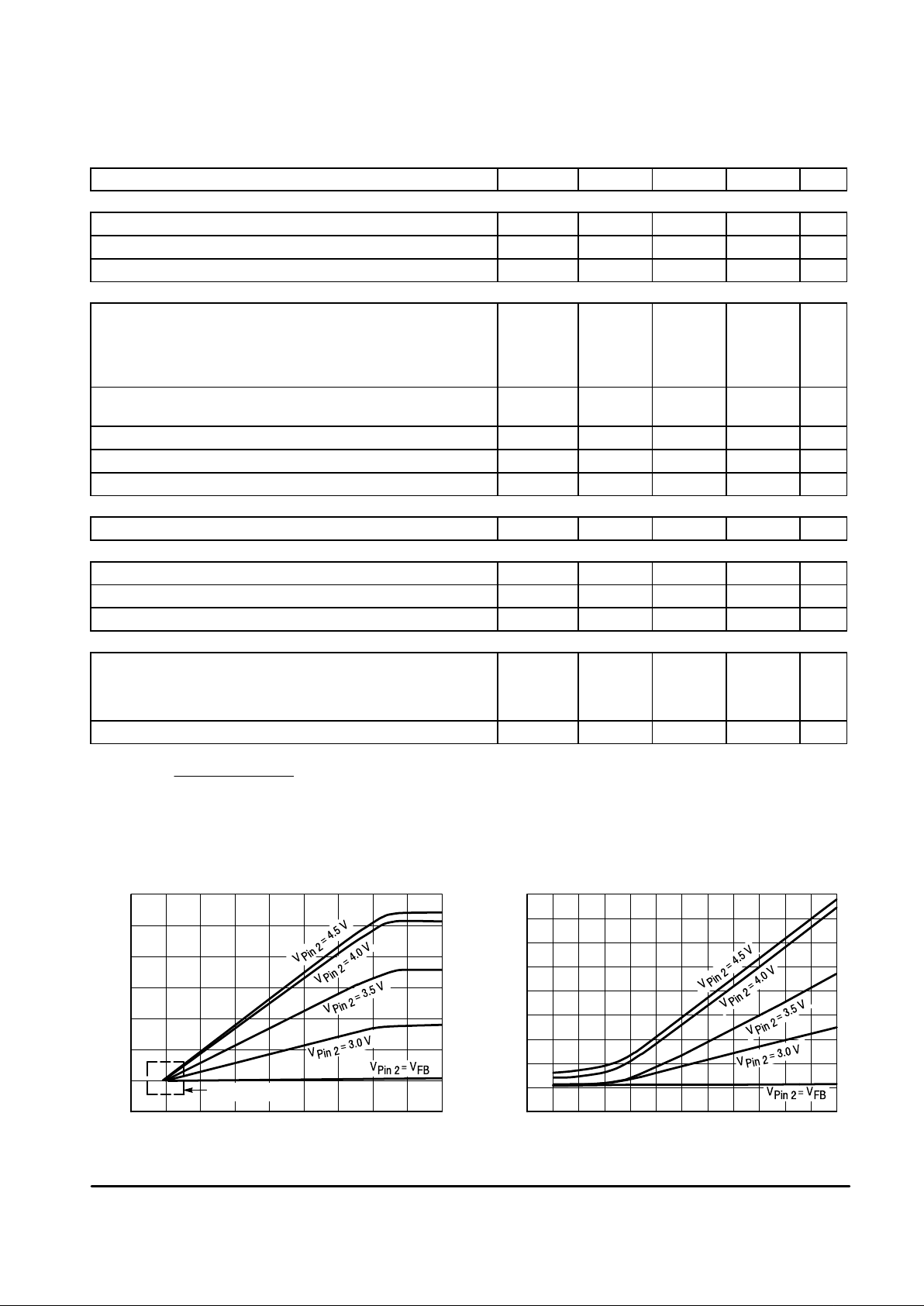
Figure 3. Voltage Feedback Input Threshold
Change versus Temperature
0 0.5 1.0 1.5
I
Sink
, OUTPUT SINK CURRENT (mA)
V
sat
, OUTPUT SA TURATION VOLTAGE (V)
Figure 4. Error Amp Open Loop Gain and
Phase versus Frequency
Gain
Phase
A
VOL
, OPEN LOOP VOL TAGE GAIN (dB)
100
80
60
40
20
–20
10
f, FREQUENCY (Hz)
100 1.0 k 10 k 100 k 1.0 M 10 M
0
φ
, EXCESS PHASE ( C)
120
180
150
Figure 5. Error Amp Small Signal
Transient Response
V
FB
, VOLTAGE FEEDBACK THRESHOLD CHANGE (mV)
+4.0
–55
TA, AMBIENT TEMPERATURE (
°
C)
–4.0
–8.0
–12
–16
–25 0 25 50 75 100 125
∆
0
Figure 6. Error Amp Large Signal
Transient Response
Figure 7. Error Amp Output Saturation
versus Sink Current
–55
TA, AMBIENT TEMPERATURE (°C)
–25 0 25 50 75 100 125
Figure 8. Restart Time Delay versus Temperature
t
DLY
, RESTART TIME DELAY ( s)
µ
2.0
°
0
30
60
90
2.55 V
2.5 V
2.45 V
0.5
µ
s/DIV
20 mV/DIV
VCC = 12 V
AV = –1.0
TA = 25
°
C
VCC = 12 V
AV = –1.0
TA = 25
°
C
200 mV/DIV
1.0 µs/DIV
3.0 V
2.5 V
2.0 V
VCC = 12 V
Pins 1 to 2
VCC = 12 V
VO = 3.0 V to 3.5 V
RL = 100 k
TA = 25
°
C
5.0
4.0
3.0
2.0
1.0
0
525
475
425
375
325
275
VCC = 12 V
VFB = 2.7 V
TA = 25
°
C
VCC = 12 V
 Loading...