

Motorola MC34261P, MC34261D Datasheet
The MC34261/MC33261 are active power factor controllers specifically
designed for use as a preconverter in electronic ballast and in off–line power
converter applications. These integrated circuits feature an internal startup
timer, a one quadrant multiplier for near unity power factor, zero current
detector to ensure critical conduction operation, high gain error amplifier,
trimmed internal bandgap reference, current sensing comparator, and a
totem pole output ideally suited for driving a power MOSFET.
Also included are protective features consisting of input undervoltage
lockout with hysteresis, cycle–by–cycle current limiting, and a latch for single
pulse metering. These devices are available in dual–in–line and surface
mount plastic packages.
• Internal Startup Timer
• One Quadrant Multiplier
• Zero Current Detector
• Trimmed 2% Internal Bandgap Reference
• Totem Pole Output
• Undervoltage Lockout with Hysteresis
• Low Startup and Operating Current
• Pinout Equivalent to the SG3561
• Functional Equivalent to the TDA4817
Order this document by MC34261/D
POWER FACTOR
CONTROLLERS
SEMICONDUCTOR
TECHNICAL DATA
P SUFFIX
PLASTIC PACKAGE
8
1
8
1
CASE 626
D SUFFIX
PLASTIC PACKAGE
CASE 751
(SO–8)
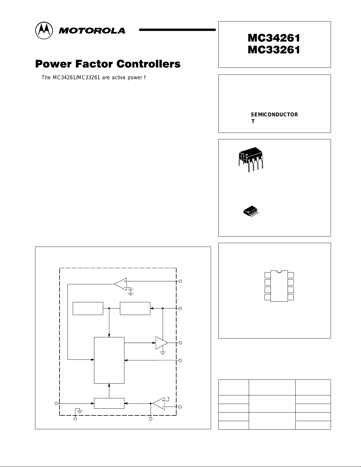
Multiplier
Input
Simplified Block Diagram
PIN CONNECTIONS
Voltage Feedback
Zero Current Detector
&
Undervoltage
Lockout
Error Amp
Compensation
V
2
2.5V
Reference
Multiplier,
Latch,
PWM,
Timer,
Logic
3
6
Gnd
Multiplier
ref
Zero Current
Detect Input
5
V
CC
8
Drive Output
7
Current Sense
Input
4
Voltage
Feedback
1
Input
Compensation
Multiplier Input
Current Sense
ORDERING INFORMATION
Device
MC34261D
MC34261P
MC33261D
MC33261P
1
Input
2
3
4
Input
(Top View)
Operating
Temperature Range
TA = 0° to +70°C
TA = –40° to +85°C
V
8
CC
Drive Output
7
Gnd
6
Zero Current
5
Detect Input
Package
Plastic DIP
Plastic DIP
SO–8
SO–8
MOTOROLA ANALOG IC DEVICE DATA
Motorola, Inc. 1996 Rev 1
1
MC34261 MC33261
MAXIMUM RATINGS
Rating Symbol Value Unit
Total Power Supply and Zener Current (ICC + IZ) 30 mA
Output Current, Source or Sink (Note 1) I
Current Sense, Multiplier, and V oltage Feedback Inputs V
Zero Current Detect Input
High State Forward Current
Low State Reverse Current
Power Dissipation and Thermal Characteristics
P Suffix, Plastic Package Case 626
Maximum Power Dissipation @ TA = 70°C
Thermal Resistance, Junction–to–Air
R
D Suffix, Plastic Package Case 626
Maximum Power Dissipation @ TA = 70°C
Thermal Resistance, Junction–to–Air
R
Operating Junction Temperature T
Operating Ambient Temperature (Note 3)
MC34261
MC33261
Storage Temperature T
O
I
in
P
θJA
P
θJA
T
stg
in
D
D
J
A
500 mA
–1.0 to 10 V
50
–10
800
100
450
178
+150 °C
0 to +70
–40 to +85
–55 to +150 °C
mA
mW
°C/W
mW
°C/W
°C
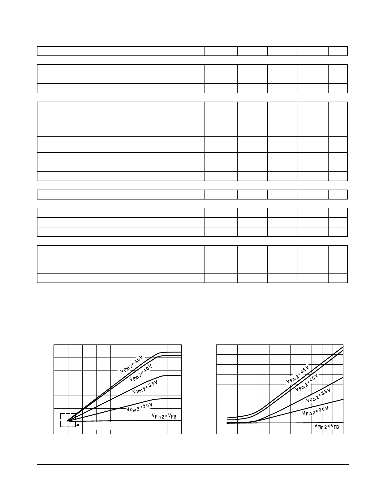
ELECTRICAL CHARACTERISTICS (V
= 12 V, for typical values TA = 25°C, for min/max values TA is the operating ambient
CC
temperature range that applies [Note 3], unless otherwise noted.)
Characteristic
Symbol Min Typ Max Unit
ERROR AMPLIFIER
Voltage Feedback Input Threshold
TA = 25°C
TA = T
low
to T
(VCC = 12 V to 28 V)
high
Line Regulation (VCC = 12 V to 28 V, TA = 25°C) Reg
Input Bias Current (VFB = 0 V) I
Open Loop Voltage Gain A
V
FB
IB
VOL
line
2.465
2.44
2.5 2.535
2.54
– 1.0 10 mV
– –0.3 –1.0 µA
65 85 – dB
Gain Bandwidth Product (TA = 25°C) GBW 0.7 1.0 – MHz
Output Source Current (VO = 4.0 V, VFB = 2.3 V) I
Source
0.25 0.5 0.75 mA
Output Voltage Swing
High State (I
Low State (I
= 0.2 mA, VFB = 2.3 V)
Source
= 0.4 mA, VFB = 2.7 V)
Sink
V
OH
V
OL
5.0
–
2.1
5.7
–
2.44
MULTIPLIER
Dynamic Input Voltage Range
Multiplier Input (Pin 3)
Compensation (Pin 2)
Input Bias Current (VFB = 0 V) I
Multiplier Gain (V
Pin 3
= 0.5 V, V
= VFB + 1.0 V) (Note 2) K 0.4 0.62 0.8 1/V
Pin 2
V
V
Pin 3
Pin 2
IB
0 to 2.5
VFB to
(VFB + 1.0)
0 to 3.5
VFB to
(VFB + 1.5)
–
–
– –0.3 –1.0 µA
ZERO CURRENT DETECTOR
Input Threshold Voltage (Vin Increasing) V
Hysteresis (Vin Decreasing) V
th
H
1.3 1.6 1.8 V
40 110 200 mV
Input Clamp Voltage
High State (I
Low State (I
NOTES: 1. Maximum package power dissipation limits must be observed.
2. K =
3. T
low
3. T
low
= 3.0 mA)
DET
= –3.0 mA)
DET
Pin 4 Threshold Voltage
V
Pin 3(VPin 2
= –40°C for MC34261
= –40°C for MC33261
– VFB)
T
= +70°C for MC34261
high
T
= +85°C for MC33261
high
V
IH
V
IL
6.1
0.3
6.7
0.7
–
1.0
V
V
V
V
2
MOTOROLA ANALOG IC DEVICE DATA
MC34261 MC33261
ELECTRICAL CHARACTERISTICS (V
= 12 V, for typical values TA = 25°C, for min/max values TA is the operating ambient
CC
temperature range that applies [Note 3], unless otherwise noted.)
Characteristic
CURRENT SENSE COMPARATOR
Input Bias Current (V
Input Offset Voltage (V
Delay to Output t
= 0 V) I
Pin 4
Pin 2
= 1.1 V, V
= 0 V) V
Pin 3
PHL (in/out)
DRIVE OUTPUT
Output Voltage (VCC = 12 V)
Low State (I
Low State (I
High State (I
High State (I
Output Voltage (VCC = 30 V)
High State (I
= 20 mA)
Sink
= 200 mA)
Sink
= 20 mA)
Source
= 200 mA)
Source
= 20 mA, CL = 15 pF)
Source
V
Output Voltage Rise T ime (CL = 1.0 nF) t
Output Voltage Fall T ime (CL = 1.0 nF) t
Output Voltage with UVLO Activated (VCC = 7.0 V, I
= 1.0 mA) V
Sink
OH(UVLO)
RESTART TIMER
Restart Time Delay t
UNDERVOLTAGE LOCKOUT
Startup Threshold (VCC Increasing) V
Minimum Operating Voltage After Turn–On (VCC Decreasing) V
Hysteresis V
TOTAL DEVICE
Power Supply Current
Startup (VCC = 7.0 V)
Operating
Dynamic Operating (50 kHz, CL = 1.0 nF)
Power Supply Zener Voltage V
NOTES: 1. Maximum package power dissipation limits must be observed.
Pin 4 Threshold Voltage
2. K =
V
3. T
3. T
Pin 3(VPin 2
= –40°C for MC34261
low
= –40°C for MC33261
low
– VFB)
T
= +70°C for MC34261
high
T
= +85°C for MC33261
high
Symbol Min Typ Max Unit
IB
IO
– –0.5 –2.0 µA
– 3.5 15 mV
– 200 400 ns
V
V
OL
V
OH
O(max)
r
f
–
1.8
9.8
7.8
0.3
2.4
10.3
8.3
0.8
3.3
–
8.8
14 16 18
– 50 120 ns
– 50 120 ns
V
– 0.2 0.8 V
DLY
th
Shutdown
H
I
CC
Z
150 400 – µs
9.2 10.0 10.8 V
7.0 8.0 9.0 V
1.75 2.0 2.5 V
mA
–
–
–
0.3
7.1
9.0
0.5
12
20
30 36 – V
Figure 1. Current Sense Input Threshold
versus Multiplier Input
3.0
2.5
2.0
1.5
1.0
0.5
0
, CURRENT SENSE THRESHOLD VOLTAGE (V)
CS
–0.5
V
–0.5 4.0
See Figure 2
1.0 1.5
VM, MULTIPLIER INPUT VOLTAGE (V)
MOTOROLA ANALOG IC DEVICE DATA
, CURRENT SENSE THRESHOLD VOLTAGE (V)
V
CS
0.16
0.14
0.12
0.10
0.08
0.06
0.04
0.02
–0.02
–0.12
Figure 2. Current Sense Input Threshold
versus Multiplier Input
0
–0.08 0 0.04 0.08 0.120 0.5 2.0 2.5 3.0 3.5 –0.04
VM, MULTIPLIER INPUT VOLTAGE (V)
3
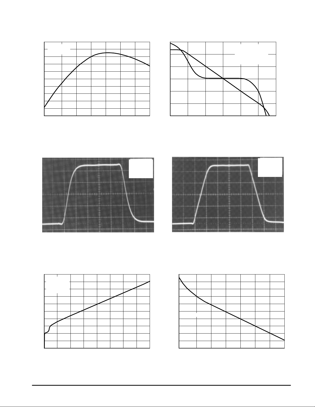
MC34261 MC33261
Figure 3. V oltage Feedback Input Threshold
Change versus T emperature
+4.0
VCC = 12 V
Pins 1 to 2
0
–4.0
–8.0
–12
, VOLTAGE FEEDBACK THRESHOLD CHANGE (mV)
FB
–16
V
–55
∆
–25 0 25 50 75 100 125
TA, AMBIENT TEMPERATURE (
Figure 5. Error Amp Small Signal
Transient Response
2.55 V
°
C)
VCC = 12 V
AV = –1.0
°
C
TA = 25
Figure 4. Error Amp Open Loop Gain and
100
80
60
40
20
, OPEN LOOP VOL TAGE GAIN (dB)
0
VOL
A
–20
10
3.0 V
100 1.0 k 10 k 100 k 1.0 M 10 M
Phase versus Frequency
VCC = 12 V
VO = 3.0 V to 3.5 V
Gain
f, FREQUENCY (Hz)
RL = 100 k
°
C
TA = 25
Figure 6. Error Amp Large Signal
Transient Response
VCC = 12 V
Phase
AV = –1.0
°
TA = 25
0
30
°
60
90
120
, EXCESS PHASE ( C)
φ
150
180
C
2.5 V
2.45 V
0.5
µ
Figure 7. Error Amp Output Saturation
versus Sink Current
5.0
VCC = 12 V
VFB = 2.7 V
4.0
3.0
2.0
1.0
, OUTPUT SA TURATION VOLTAGE (V)
sat
V
0
0 0.5 1.0 1.5
TA = 25
°
C
I
, OUTPUT SINK CURRENT (mA)
Sink
s/DIV
2.0
2.5 V
20 mV/DIV
2.0 V
525
µ
475
425
375
, RESTART TIME DELAY ( s)
325
DLY
t
275
1.0 µs/DIV
Figure 8. Restart Time Delay versus Temperature
VCC = 12 V
–55
–25 0 25 50 75 100 125
TA, AMBIENT TEMPERATURE (°C)
200 mV/DIV
4
MOTOROLA ANALOG IC DEVICE DATA
 Loading...