Datasheet MC34064DM-5, MC34064DM-5R2, MC34064P-005, MC34064P-5, MC34064D-005 Datasheet (Motorola)
...
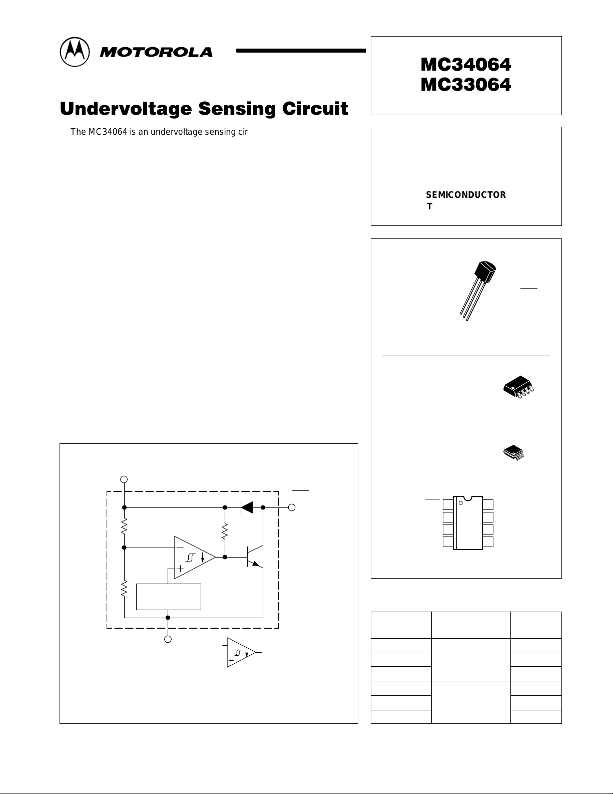
The MC34064 is an undervoltage sensing circuit specifically designed for
use as a reset controller in microprocessor-based systems. It offers the
designer an economical solution for low voltage detection with a single
external resistor. The MC34064 features a trimmed-in-package bandgap
reference, and a comparator with precise thresholds and built-in hysteresis
to prevent erratic reset operation. The open collector reset output is capable
of sinking in excess of 10 mA, and operation is guaranteed down to 1.0 V
input with low standby current. These devices are packaged in 3-pin
TO-226AA, 8-pin SO–8 and Micro–8 surface mount packages.
Applications include direct monitoring of the 5.0 V MPU/logic power
supply used in appliance, automotive, consumer and industrial equipment.
• Trimmed-In-Package Temperature Compensated Reference
• Comparator Threshold of 4.6 V at 25°C
• Precise Comparator Thresholds Guaranteed Over Temperature
• Comparator Hysteresis Prevents Erratic Reset
• Reset Output Capable of Sinking in Excess of 10 mA
• Internal Clamp Diode for Discharging Delay Capacitor
• Guaranteed Reset Operation with 1.0 V Input
• Low Standby Current
• Economical TO–226AA, SO–8 and Micro–8 Surface Mount Packages
Order this document by MC34064/D
UNDERVOLTAGE
SENSING CIRCUIT
SEMICONDUCTOR
TECHNICAL DATA
P SUFFIX
PLASTIC PACKAGE
CASE 29
(TO–226AA)
D SUFFIX
PLASTIC PACKAGE
CASE 751
(SO–8)
Pin 1. Reset
2. Input
1
2
3
3. Ground
8
1
Representative Block Diagram
Input
Pin numbers adjacent to terminals are for the 3–pin TO–226AA package.
Pin numbers in parenthesis are for the 8–lead packages.
2 (2)
1.2 V
ref
3 (4)
Gnd
=
This device contains 21 active transistors.
Reset
1 (1)
Sink Only
Positive True Logic
DM SUFFIX
PLASTIC PACKAGE
CASE 846A
(Micro–8)
1
Reset
2
Input
3
N.C.
4
Ground
(Top View)
8
1
8
N.C.
7
N.C.
6
N.C.
5
N.C.
ORDERING INFORMATION
Operating
Device
MC34064D–5
MC34064DM–5 Micro–8
MC34064P–5 TO–226AA
MC33064D–5 SO–8
MC33064DM–5 Micro–8
MC33064P–5 TO–226AA
Temperature Range
TA = 0° to +70°C
TA = – 40° to +85°C
Package
SO–8
MOTOROLA ANALOG IC DEVICE DATA
Motorola, Inc. 1996 Rev 2
1

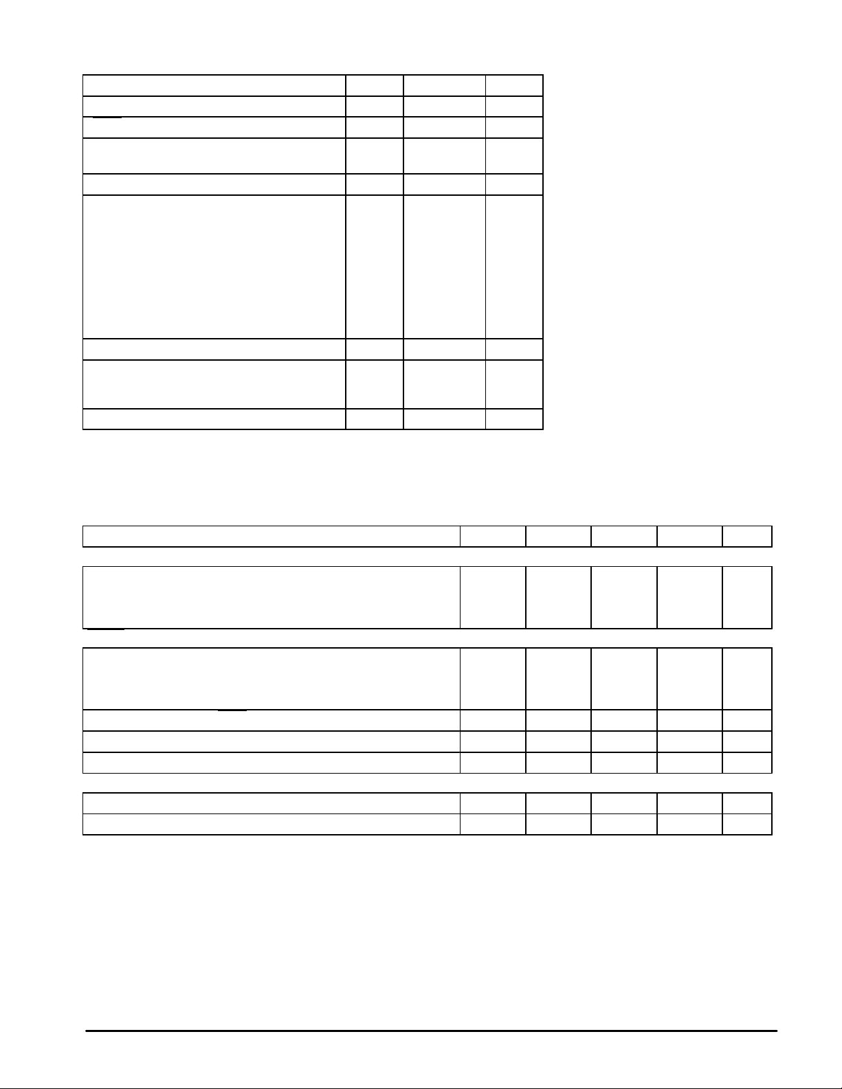
MAXIMUM RATINGS
Rating Symbol Value Unit
Power Input Supply Voltage V
Reset Output Voltage V
Reset Output Sink Current (Note 1) I
Clamp Diode Forward Current, Pin 1 to 2 (Note 1) I
Power Dissipation and Thermal Characteristics
P Suffix, Plastic Package
Maximum Power Dissipation @ TA = 25°C
Thermal Resistance, Junction–to–Air
D Suffix, Plastic Package
Maximum Power Dissipation @ TA = 25°C
Thermal Resistance, Junction–to–Air
DM Suffix, Plastic Package
Maximum Power Dissipation @ TA = 25°C
Thermal Resistance, Junction–to–Air
Operating Junction Temperature T
Operating Ambient Temperature
MC34064
MC33064
Storage Temperature Range T
NOTE: ESD data available upon request.
MC34064 MC33064
–1.0 to 10 V
10 V
Internally
Limited
100 mA
625
200
625
200
520
240
+150 °C
0 to +70
–40 to +85
–65 to +150 °C
Sink
P
R
P
R
P
R
F
θJA
θJA
θJA
T
stg
in
O
D
D
D
J
A
mA
mW
°C/W
mW
°C/W
mW
°C/W
°C
ELECTRICAL CHARACTERISTICS (For typical values T
= 25°C, for min/max values TA is the operating ambient temperature range
A
that applies [Notes 2 and 3] unless otherwise noted.)
Characteristics Symbol Min Typ Max Unit
COMPARATOR
Threshold Voltage
High State Output (Vin Increasing)
Low State Output (Vin Decreasing)
Hysteresis
V
IH
V
IL
V
H
0.01
RESET OUTPUT
Output Sink Saturation
(Vin = 4.0 V, I
(Vin = 4.0 V, I
(Vin = 1.0 V, I
Sink
Sink
Sink
= 8.0 mA)
= 2.0 mA)
= 0.1 mA)
Output Sink Current (Vin, Reset = 4.0 V) I
Output Off-State Leakage (Vin, Reset = 5.0 V) I
Clamp Diode Forward Voltage, Pin 1 to 2 (IF = 10 mA) V
V
OL
Sink
OH
F
TOTAL DEVICE
Operating Input Voltage Range V
Quiescent Input Current (Vin = 5.0 V) I
NOTES: 1. Maximum package power dissipation limits must be observed.
2.Low duty cycle pulse techniques are used during test to maintain junction temperature as close to ambient as possible.
3.T
=0°C for MC34064 T
low
–40°C for MC33064 +85°C for MC33064
= +70°C for MC34064
high
in
in
1.0 to 6.5 – – V
4.5
4.5
4.61
4.59
0.02
4.7
4.7
0.05
V
V
–
–
–
0.46
0.15
–
1.0
0.4
0.1
10 27 60 mA
– 0.02 0.5 µA
0.6 0.9 1.2 V
– 390 500 µA
2
MOTOROLA ANALOG IC DEVICE DATA

MC34064 MC33064
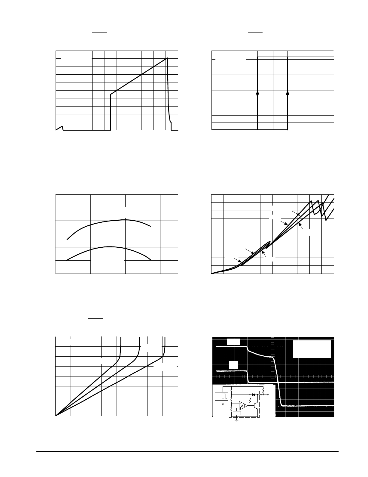
Figure 1. Reset Output Voltage versus
Input Voltage
1
RL = 10 k to V
0
TA = 25
8.0
6.0
4.0
, OUTPUT VOL TAGE (V)
O
2.0
V
0
0 2.0 4.0 6.0 8.0 1
in
°
C
Vin, INPUT VOLTAGE (V)
Figure 3. Comparator Threshold V oltage
versus T emperature
4.630
4.620
4.610
4.600
4.590
, THRESHOLD VOLTAGE (V)
th
4.580
V
RL = 10 k to V
in
Upper Threshold
High State Output
Lower Threshold
Low State Output
Figure 2. Reset Output Voltage versus
Input Voltage
5.0
RL = 10 k to V
TA = 25
4.0
3.0
2.0
, OUTPUT VOL TAGE (V)
O
1.0
V
0
0
4.56
0
in
°
C
4.58
0
Vin, INPUT VOLTAGE (V)
4.60
0
4.62
0
4.64
0
Figure 4. Input Current versus Input Voltage
1.0
0.8
0.6
0.4
, INPUT CURRENT (mA)
0.2
in
I
TA = +25
°
C
+85
°
C
TA = +25°C
–40°C
°
C
–40
+85°C
4.570
–55 –25 0 25 50 75 100 125
TA, AMBIENT TEMPERATURE (
Figure 5. Reset
Output Saturation versus
°
C)
Sink Current
2.0
V
= 4.0 V
in
1.5
1.0
, OUTPUT SA TURATION (V)
0.5
OL
V
0
010203040
TA = 85
°
C
I
, SINK CURRENT (mA)
Sink
TA = 25
°
C
TA = –40
°
C
90%
5.0 V –
4.0 V –
10%
0
0 2.0 4.0 6.0 8.0 10
Vin, INPUT VOLTAGE (V)
Delay Time
10k
Reset
200 ns/DIV
Vin = 5.0 V to 4.0 V
RL = 10 k
°
C
TA = 25
5.0V
4.0V
Figure 6. Reset
Reset
V
in
V
in
REF
MOTOROLA ANALOG IC DEVICE DATA
3

MC34064 MC33064
Figure 7. Clamp Diode Forward Current
versus V oltage
80
Vin = 0 V
°
C
TA = 25
60
40
20
, FORWARD CURRENT (mA)
F
I
0
0 0.4 0.8 1.2 1.6
VF, FORWARD VOLTAGE (V)
Figure 8. Low V oltage Microprocessor Reset
+
2 (2)
Power
Supply
–
–
+
1.2 V
ref
3 (4)
Figure 9. Low V oltage Microprocessor Reset with Additional Hysteresis
R
H
+
Power
Supply
–
Comparator hysteresis can be increased with the addition of resistor R
simplified and does not account for the change of input current I
(Figure 4). An increase of the lower threshold
4.59 V. The equations are accurate to
I
in
2 (2)
1 (1)
R
L
Reset
–
+
1.2V
ref
3 (4)
as VCC crosses the comparator threshold
∆
V
th(lower)
±
10% with RH less than 150 Ω and RL between 1.5 kΩ and 10 k
in
will be observed due to Iin which is typically 340 µA at
4.6 R
VH
≈
∆
V
th(lower)
Where: RH ≤ 150
Where: RL ≥ 1.5 Ω, ≤ 10 k
. The hysteresis equation has been
H
R
1 (1)
C
Reset
DLY
Microprocessor
Circuit
A time delayed reset can be accomplished with the
addition of C
power supply rise times (<500 ns) it is recommended
that the RC
V
th(MPU)
. For systems with extremely fast
DLY
time constant be greater than 5.0
DLY
is the microprocessor reset input threshold.
1
V
th(MPU)
1 –
V
in
V
H
(mV)
20 0 0 0
51 3.4 10 1.5
40 6.8 20 4.7
81 6.8 20 1.5
71 10 30 2.7
112 10 30 1.5
100 16 47 2.7
164 16 47 1.5
190 34 100 2.7
327 34 100 1.5
276 51 150 2.7
480 51 150 1.5
H
+ 0.02
R
L
≈ 340 RH x 10
t
= RC
DLY
Microprocessor
Circuit
–6
Ω
Ω
DLY
In
Ω.
µ
s.
Test Data
∆V
th
(mV)
R
(Ω)
R
H
(kΩ)
L
4
MOTOROLA ANALOG IC DEVICE DATA

MC34064 MC33064
Figure 10. V oltage Monitor Figure 11. Solar Powered Battery Charger
+
Power
Supply
–
Vin = 11.5
to 14.5V
4.7k
2 (2)
470
1.2V
2 (2)
–
+
ref
3 (4)
+
1.2V
ref
1.0k
1 (1)
+
–
2 (2)
1.2V
–
+
ref
3 (4)
1 (1)
Solar
Cells
Figure 12. Low Power Switching Regulator
25
µ
H
MPSW51A
470
68022
+
330
1 (1)
–
+
1N5819
1.2k
1N756
VO = 5.0 V
IO = 50 mA
+
Test Conditions Results
Line Regulation Vin = 11.5 V to 14.5 V, IO = 50 mA 35 mV
Load Regulation Vin = 12.6 V, IO = 0 mA to 50 mA 12 mV
Output Ripple Vin = 12.6 V, IO = 50 mA 60 mVpp
Efficiency Vin = 12.6 V, IO = 50 mA 77%
3 (4)
Figure 13. MOSFET Low Voltage Gate Drive Protection
V
CC
R
L
4.6V
2 (2)
–
+
1.2V
ref
3 (4)
Overheating of the logic level power MOSFET due to insufficient gate voltage can be prevented with the above
circuit. When the input signal is below the 4.6 V threshold of the MC34064, its output grounds the gate of the L
MOSFET .
270
1 (1)
MTP3055EL
2
MOTOROLA ANALOG IC DEVICE DATA
5

SEATING
PLANE
MC34064 MC33064
OUTLINE DIMENSIONS
P SUFFIX
PLASTIC PACKAGE
CASE 29–04
A
B
(TO–226AA)
ISSUE AD
R
P
L
XX
H
V
1
F
G
K
D
J
C
SECTION X–X
N
N
NOTES:
1. DIMENSIONING AND TOLERANCING PER ANSI
Y14.5M, 1982.
2. CONTROLLING DIMENSION: INCH.
3. CONTOUR OF PACKAGE BEYOND DIMENSION R
IS UNCONTROLLED.
4. DIMENSION F APPLIES BETWEEN P AND L.
DIMENSION D AND J APPLY BETWEEN L AND K
MINIMUM. LEAD DIMENSION IS UNCONTROLLED
IN P AND BEYOND DIMENSION K MINIMUM.
DIM MIN MAX MIN MAX
A 0.175 0.205 4.45 5.20
B 0.170 0.210 4.32 5.33
C 0.125 0.165 3.18 4.19
D 0.016 0.022 0.41 0.55
F 0.016 0.019 0.41 0.48
G 0.045 0.055 1.15 1.39
H 0.095 0.105 2.42 2.66
J 0.015 0.020 0.39 0.50
K 0.500 ––– 12.70 –––
L 0.250 ––– 6.35 –––
N 0.080 0.105 2.04 2.66
P ––– 0.100 ––– 2.54
R 0.115 ––– 2.93 –––
V 0.135 ––– 3.43 –––
MILLIMETERSINCHES
–T–
–B–
D SUFFIX
PLASTIC PACKAGE
CASE 751–05
(SO–8)
ISSUE P
–A–
58
1
4
M
B
M
4X P
0.25 (0.010)
J
_
X 45
R
G
_
M
C
SEATING
K
8X D
PLANE
SS
A0.25 (0.010)MTB
F
NOTES:
1. DIMENSIONS A AND B ARE DATUMS AND T IS A
DATUM SURFACE.
2. DIMENSIONING AND TOLERANCING PER ANSI
Y14.5M, 1982.
3. DIMENSIONS ARE IN MILLIMETER.
4. DIMENSION A AND B DO NOT INCLUDE MOLD
PROTRUSION.
5. MAXIMUM MOLD PROTRUSION 0.15 PER SIDE.
6. DIMENSION D DOES NOT INCLUDE MOLD
PROTRUSION. ALLOWABLE DAMBAR
PROTRUSION SHALL BE 0.127 TOTAL IN EXCESS
OF THE D DIMENSION AT MAXIMUM MATERIAL
CONDITION.
MILLIMETERS
DIM MIN MAX
A 4.80 5.00
B 3.80 4.00
C 1.35 1.75
D 0.35 0.49
F 0.40 1.25
G 1.27 BSC
J 0.18 0.25
K 0.10 0.25
M 0 7
P 5.80 6.20
R 0.25 0.50
__
6
MOTOROLA ANALOG IC DEVICE DATA

PIN 1 ID
SEATING
PLANE
–T–
0.038 (0.0015)
MC34064 MC33064
OUTLINE DIMENSIONS
DM SUFFIX
PLASTIC PACKAGE
CASE 846A–02
(Micro–8)
–A–
K
G
–B–
8 PL
D
0.08 (0.003) A
M
C
H
J
ISSUE B
S
B
T
S
L
NOTES:
1. DIMENSIONING AND TOLERANCING PER ANSI
Y14.5M, 1982.
2. CONTROLLING DIMENSION: MILLIMETER.
3. DIMENSION A DOES NOT INCLUDE MOLD FLASH,
PROTRUSIONS OR GATE BURRS. MOLD FLASH,
PROTRUSIONS OR GATE BURRS SHALL NOT
EXCEED 0.15 (0.006) PER SIDE.
4. DIMENSION D DOES NOT INCLUDE INTERLEAD
FLASH OR PROTRUSION. INTERLEAD FLASH OR
PROTRUSION SHALL NOT EXCEED 0.25 (0.010)
PER SIDE.
DIM MIN MAX MIN MAX
A 2.90 3.10 0.114 0.122
B 2.90 3.10 0.114 0.122
C ––– 1.10 ––– 0.043
D 0.25 0.40 0.010 0.016
G 0.65 BSC 0.026 BSC
H 0.05 0.15 0.002 0.006
J 0.13 0.23 0.005 0.009
K 4.75 5.05 0.187 0.199
L 0.40 0.70 0.016 0.028
INCHESMILLIMETERS
MOTOROLA ANALOG IC DEVICE DATA
7

MC34064 MC33064
Motorola reserves the right to make changes without further notice to any products herein. Motorola makes no warranty , representation or guarantee regarding
the suitability of its products for any particular purpose, nor does Motorola assume any liability arising out of the application or use of any product or circuit, and
specifically disclaims any and all liability, including without limitation consequential or incidental damages. “T ypical” parameters which may be provided in Motorola
data sheets and/or specifications can and do vary in different applications and actual performance may vary over time. All operating parameters, including “Typicals”
must be validated for each customer application by customer’s technical experts. Motorola does not convey any license under its patent rights nor the rights of
others. Motorola products are not designed, intended, or authorized for use as components in systems intended for surgical implant into the body, or other
applications intended to support or sustain life, or for any other application in which the failure of the Motorola product could create a situation where personal injury
or death may occur. Should Buyer purchase or use Motorola products for any such unintended or unauthorized application, Buyer shall indemnify and hold Motorola
and its officers, employees, subsidiaries, affiliates, and distributors harmless against all claims, costs, damages, and expenses, and reasonable attorney fees
arising out of, directly or indirectly, any claim of personal injury or death associated with such unintended or unauthorized use, even if such claim alleges that
Motorola was negligent regarding the design or manufacture of the part. Motorola and are registered trademarks of Motorola, Inc. Motorola, Inc. is an Equal
Opportunity/Affirmative Action Employer.
How to reach us:
USA/EUROPE/ Locations Not Listed: Motorola Literature Distribution; JAPAN: Nippon Motorola Ltd.; Tatsumi–SPD–JLDC, 6F Seibu–Butsuryu–Center,
P.O. Box 20912; Phoenix, Arizona 85036. 1–800–441–2447 or 602–303–5454 3–14–2 Tatsumi Koto–Ku, Tokyo 135, Japan. 03–81–3521–8315
MFAX: RMF AX0@email.sps.mot.com – TOUCHT ONE 602–244–6609 ASIA/PACIFIC: Motorola Semiconductors H.K. Ltd.; 8B Tai Ping Industrial Park,
INTERNET: http://Design–NET.com 51 Ting Kok Road, Tai Po, N.T., Hong Kong. 852–26629298
8
◊
MOTOROLA ANALOG IC DEVICE DATA
MC34064/D
*MC34064/D*
 Loading...