

Page 1
Single
T
70°C
Dual
T
0° to +70°C
查询MC34001供应商
Order this document by MC34001/D
These low cost JFET input operational amplifiers combine two
state–of–the–art analog technologies on a single monolithic integrated
circuit. Each internally compensated operational amplifier has well matched
high voltage JFET input devices for low input offset voltage. The BIFET
technology provides wide bandwidths and fast slew rates with low input bias
currents, input offset currents, and supply currents.
The Motorola BIFET family offers single, dual and quad operational
amplifiers which are pin–compatible with the industry standard MC1741,
MC1458, and the MC3403/LM324 bipolar devices. The MC34001/
34002/34004 series are specified from 0° to +70°C.
• Input Offset Voltage Options of 5.0 mV and 10 mV Maximum
• Low Input Bias Current: 40 pA
• Low Input Offset Current: 10 pA
• Wide Gain Bandwidth: 4.0 MHz
• High Slew Rate: 13 V/µs
• Low Supply Current: 1.4 mA per Amplifier
• High Input Impedance: 10
12
Ω
• High Common Mode and Supply Voltage Rejection Ratios: 100 dB
• Industry Standard Pinouts
JFET INPUT
OPERATIONAL AMPLIFIERS
8
1
P SUFFIX
PLASTIC PACKAGE
CASE 626
PIN CONNECTIONS
Offset Null
Inv. Input
Noninv. Input
Inputs A
1
2
3
4
V
EE
MC34001 (Top View)
Output A V
1
2
+
3
4
V
EE
MC34002 (Top View)
+
–
8
1
D SUFFIX
PLASTIC PACKAGE
CASE 751
(SO–8)
8
NC
7
V
CC
Output
6
5
Offset Null
8
CC
7
Output B
6
–
Inputs B
+
5
ORDERING INFORMATION
Op Amp
Function
Quad MC34004BP, P TA = 0° to +70°C Plastic DIP
Device
MC34001BD, D
MC34001BP, P
MC34002BD, D
MC34002BP, P
MOTOROLA ANALOG IC DEVICE DATA
Operating
Temperature Range
°
= 0° to+
A
=
A
°
°
°
Package
SO–8
Plastic DIP
SO–8
Plastic DIP
P SUFFIX
14
1
PLASTIC PACKAGE
CASE 646
PIN CONNECTIONS
Output 1
Inputs 1
Inputs 2
Output 2
Motorola, Inc. 1996 Rev 1
1
2
–
+
1
3
4
V
CC
5
+
–
23
6
78
MC34004 (Top View)
14
Output 4
13
–
+
4
12
11
V
EE
10
+
–
9
Output 3
Inputs 4
Inputs 3
1
Page 2
MC34001, B MC34002, B MC34004, B
MAXIMUM RATINGS
Rating Symbol Value Unit
Supply Voltage VCC, V
Differential Input Voltage (Note 1) V
Input Voltage Range V
Open Short Circuit Duration t
Operating Ambient Temperature Range T
Operating Junction Temperature T
Storage Temperature Range T
NOTES: 1.Unless otherwise specified, the absolute maximum negative input voltage is equal to the
negative power supply.
EE
ID
IDR
SC
A
J
stg
±18 V
±30 V
±16 V
Continuous
0 to +70 °C
150 °C
–65 to +150 °C
ELECTRICAL CHARACTERISTICS (V
Characteristics
Input Offset Voltage (RS ≤ 10 k)
MC3400XB
MC3400X
Average Temperature Coefficient of Input Of fset Voltage
RS ≤ 10 k, TA = T
Input Offset Current (VCM = 0) (Note 3)
MC3400XB
MC3400X
Input Bias Current (VCM = 0) (Note 3)
MC3400XB
MC3400X
Input Resistance r
Common Mode Input Voltage Range V
Large Signal Voltage Gain (VO = ±10 V, RL = 2.0 k)
MC3400XB
MC3400X
Output Voltage Swing
(RL ≥ 10 k)
(RL ≥ 2.0 k)
Common Mode Rejection Ratio (RS ≤ 10 k)
MC3400XB
MC3400X
Supply Voltage Rejection Ratio (RS ≤ 10 k) (Note 4)
MC3400XB
MC3400X
Supply Current (Each Amplifier)
MC3400XB
MC3400X
low
to T
high
(Note 2)
= +15 V, VEE = –15 V, TA = 25°C, unless otherwise noted.)
CC
Symbol Min Typ Max Unit
V
IO
—
—
∆VIO/∆T — 10 — µV/°C
I
IO
—
—
I
IB
—
—
— 10
±11
—
50
A
i
ICR
VOL
25
V
O
±12
±10
CMRR
80
70
PSRR
80
70
I
D
—
—
3.0
5.0
25
25
50
50
+15
–12
150
100
±14
±13
100
100
100
100
1.4
1.4
12
5.0
10
100
100
200
200
— Ω
—
—
—
—
—
—
—
—
—
—
2.5
2.7
Slew Rate (AV = 1.0) SR — 13 — V/µs
Gain–Bandwidth Product GBW — 4.0 — MHz
Equivalent Input Noise Voltage
(RS = 100 Ω, f = 1000 Hz)
Equivalent Input Noise Current (f = 1000 Hz) i
NOTES: 2.T
=0°C for MC34001/34001B T
low
0°C for MC34002 +70°C for MC34002
3.The input bias currents approximately double for every 10°C rise in junction temperature, TJ. Due to limited test time, the input bias currents are
4.Supply voltage rejection ratio is measured for both supply magnitudes increasing or decreasing simultaneously, in accordance with common practice.
0°C for MC34004/34004B +70°C for MC34004/34004B
correlated to junction temperature. Use of a heatsink is recommended if input bias current is to be kept to a minimum.
= +70°C for MC34001/34001B
high
e
n
n
— 25 —
— 0.01 —
mV
pA
pA
V
V/mV
V
dB
dB
mA
nV/ Hz√
pA/ Hz√
2
MOTOROLA ANALOG IC DEVICE DATA
Page 3
MC34001, B MC34002, B MC34004, B
ELECTRICAL CHARACTERISTICS (V
= +15 V, VEE = –15 V, TA = T
CC
low
to T
high
[Note 2].)
Characteristics Symbol Min Typ Max Unit
Input Offset Voltage (RS ≤ 10 k)
MC3400XB
MC3400X
Input Offset Current (VCM = 0) (Note 3)
MC3400XB
MC3400X
Input Bias Current (VCM = 0) (Note 3)
MC3400XB
MC3400X
Common Mode Input Voltage Range V
Large Signal (VO = ±10 V, RL = 2.0 k)
MC3400XB
MC3400X
Output Voltage Swing
(R ≥ 10 k)
(R ≥ 2.0 k)
Common Mode Rejection Ratio (RS ≤ 10 k)
MC3400XB
MC3400X
Supply Voltage Rejection Ratio (RS ≤ 10 k) (Note 4)
MC3400XB
MC3400X
Supply Current (Each Amplifier)
MC3400XB
MC3400X
NOTES: 2.T
=0°C for MC34001/34001B T
low
0°C for MC34002 +70°C for MC34002
3.The input bias currents approximately double for every 10°C rise in junction temperature, TJ. Due to limited test time, the input bias currents are
4.Supply voltage rejection ratio is measured for both supply magnitudes increasing or decreasing simultaneously, in accordance with common practice.
0°C for MC34004/34004B +70°C for MC34004/34004B
correlated to junction temperature. Use of a heatsink is recommended if input bias current is to be kept to a minimum.
= +70°C for MC34001/34001B
high
V
IO
I
IO
I
IB
ICR
A
VOL
V
O
CMRR
PSRR
I
D
—
—
—
—
—
—
—
—
—
—
—
—
±11 — — V
25
15
±12
±10
80
70
80
70
—
—
—
—
—
—
—
—
—
—
—
—
7.0
mV
13
nA
4.0
4.0
nA
8.0
8.0
V/mV
—
—
V
—
—
dB
—
—
dB
—
—
mA
2.8
3.0
MOTOROLA ANALOG IC DEVICE DATA
3
Page 4
MC34001, B MC34002, B MC34004, B
100
, INPUT BIAS CURRENT (nA)
IB
I
0.01
)
pp
10
1.0
0.1
40
30
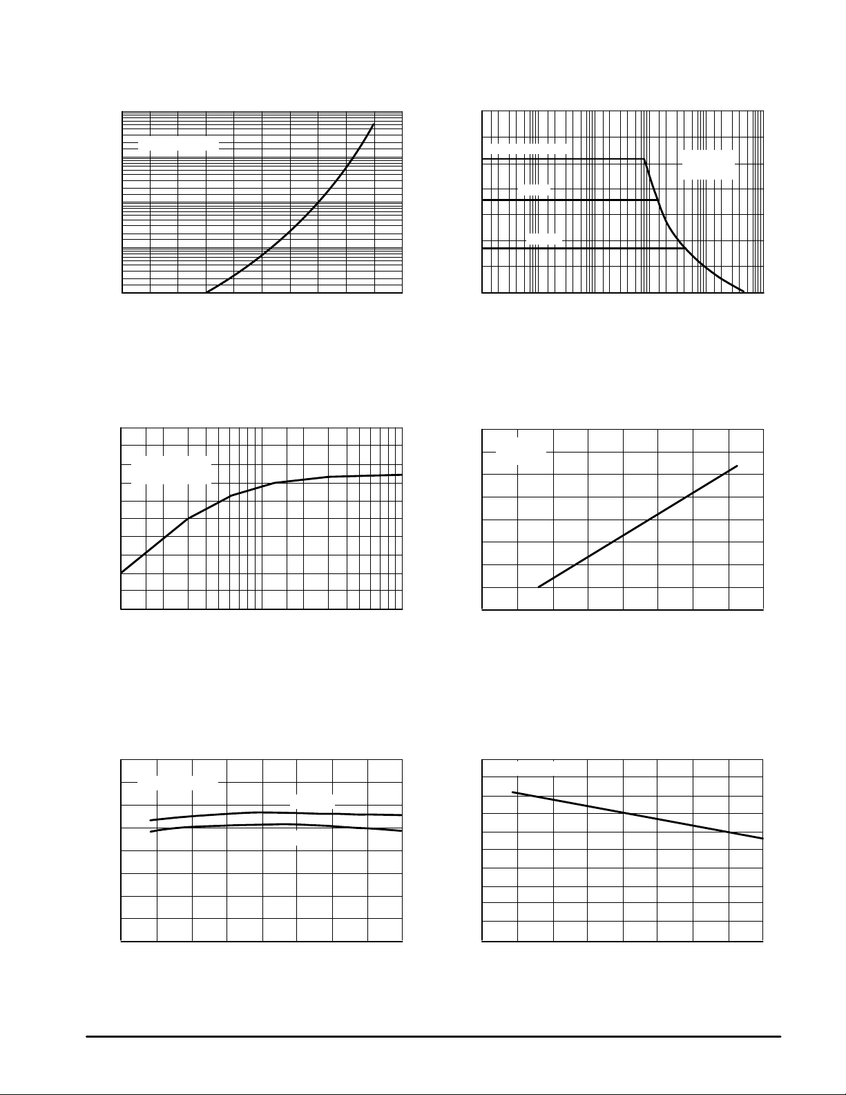
Figure 1. Input Bias Current
versus T emperature
VCC/VEE = ±15 V
–75 –50 –25 0 25 50 75 100 125
TA, AMBIENT TEMPERATURE (°C)
Figure 3. Output Voltage Swing
versus Load Resistance
VCC/VEE = ±15 V
°
C
TA = 25
Figure 2. Output Voltage Swing
versus Frequency
35
)
pp
30
VCC/VEE = ±15 V
25
20
15
10
, OUTPUT VOL TAGE SWING (V
O
5.0
V
0
100 1.0 k 10 k 100 k 1.0 M 10 M
±
10 V
±
5.0 V
f, FREQUENCY (Hz)
RL = 2.0 k
°
TA = 25
C
Figure 4. Output Voltage Swing
versus Supply V oltage
40
)
pp
30
RL = 2.0 k
°
TA = 25
C
20
20
10
5.0
, OUTPUT VOL TAGE SWING (V
O
0
0.1 0.2 0.4 0.7 1.0 2.0 10
RL, LOAD RESISTANCE (k
4.0
Ω
)
Figure 5. Output Voltage Swing
7.0
10
OUTPUT VOL TAGE SWING (V
,V
O
0
0 5.0 10 15 20
Figure 6. Supply Current per Amplifier
versus T emperature
2.0
)V
35
30
25
20
15
10
5.0
0
VCC/VEE = ±15 V
RL = 10 k
RL = 2.0 k
–50 –25 0 25 50 75 100 125
°
TA, AMBIENT TEMPERATURE (
C)
pp
, OUTPUT VOL TAGE SWING (V
O
V
1.8
1.6
1.4
1.2
1.0
0.8
0.6
0.4
D
0.2
I , SUPPLY DRAIN CURRENT (mA)
0
VCC/VEE = ±15 V
–50 –25 0 25 50 75 100 125
VCC/VEE , SUPPLY VOLTAGE (V)
versus T emperature
TA, AMBIENT TEMPERATURE (°C)
4
MOTOROLA ANALOG IC DEVICE DATA
Page 5

MC34001, B MC34002, B MC34004, B
Figure 7. Large–Signal V oltage Gain and
Phase Shift versus Frequency
±
6
10
5
10
4
10
3
10
, OPEN–LOOP GAIN
2
10
VOL
A
1
10
1
1.0 10 100 1.0 k 10 k 100 k 1.0 M 1.0 M 10 M
Phase Shift
f, FREQUENCY (Hz)
VCC/VEE =
RL = 2.0 k
TA = 25
Gain
15 V
°
C
Figure 9. Normalized Slew Rate
versus T emperature
1.15
1.10
1.05
1.00
0.95
0.90
NORMALIZED SLEW RATE
0.85
–50 –25 0 25 50 75 100 125
°
TA, AMBIENT TEMPERATURE (
C)
0
°
45
90
135
180
°
°
°
°
1000
100
PHASE SHIFT (DEGREES)
VOL
A , VOLTAGE GAIN (V/mV)
1.0
nV/ Hz )√
, EQUIVALENT INPUT NOISE VOLTAGE (
n
e
Figure 8. Large–Signal V oltage Gain
versus T emperature
VCC/VEE = ±15 V
±
10 V
VO =
RL = 2.0 k
10
–50 –25 0 25 50 75 100 125
°
TA, AMBIENT TEMPERATURE (
C)
Figure 10. Equivalent Input Noise V oltage
versus Frequency
60
50
40
30
20
10
0
0.01 0.05 0.1 0.5 1.0 5.0 10 50 100
f, FREQUENCY (kHz)
VCC/VEE = ±15 V
AV = 10
RS = 100
TA = 25°C
Ω
1.0
0.5
0.1
0.05
0.01
0.005
THD, TOT AL HARMONIC DISTORTION (%)
0.001
0.1 0.5 1.0 5.0 10 50 100
MOTOROLA ANALOG IC DEVICE DATA
Figure 11. Total Harmonic Distortion
versus Frequency
VCC/VEE = ±15 Vdc
AV = 1.0
VO = 6.0 V (RMS)
°
C
TA = 25
f, FREQUENCY (kHz)
5
Page 6

–
Inputs
+
MC34001, B MC34002, B MC34004, B
Q3
J1 J2
Representative Circuit Schematic
(Each Amplifier)
Q4 Q5
Q17
Output
Q2
Q6
Q1
Bias Circuitry
Common to All
Amplifiers
2.0 k
V
CC
Offset
Null
(MC34001 only)
1.5 k
Q12
V
CC
Q14
Q10
Q20
Q18
1.5 k
Q13
Q15
Q11
10 pF
Q19
Q21
Q16
Q22
Q23
24
Q24
Figure 12. Output Current to Voltage Transformation
for a D–to–A Converter
Q9
Q8
J3
Q7
Q25
V
EE
6
MSB
A1
A2
A3
A4
A5
A6
A7
A8LSB
D–to–A
15 pF
Settling time to within 1/2 LSB is approximately 4.0
R1
R2 VCC = 15 V
1
+
I
o
V
EE
–
VEE = –15 V
R
O
V
MC34001
C
ref
from the time all bits are switched (C = 68 pF).
The value of C may be selected to minimize overshoot
and ringing.
V
O
Theoretical V
VO =
V
R1
ref
O
A1 A2 A3 A4 A5 A6 A7 A8
(RO)
+++++++
2 4 8 16 32 64 128 256
µ
s
MOTOROLA ANALOG IC DEVICE DATA
Page 7

MC34001, B MC34002, B MC34004, B
Figure 13. Positive Peak Detector
V
in
Reset
Figure 14. Long Interval RC Timer Figure 15. Isolating Large Capacitive Loads
V
R
Run
Time (t) = R4 Cn (VR/VR–VI), R3 = R4, R5 = 0.1 R
R1 V1 R3
R4
Clear
If R1 = R2: t = 0.693 R4C
R2
2
3
C*
R5
8
V
CC
–
1/2
2
MC34002
3
+
4
V
EE
Reset
Network
or Relay
+15 V
7
MC34001
–
+
6
4
R6
–15 V
*Polycarbonate or
Polystyrene Capacitor
6
D1
1N914
6
–
1/2
MC34002
5
*
µ
F
1
+2.0 V
–2.0 V
+
*Polycarbonate capacitor
D1 = Hi–speed, low–reverse leakage diode
0
Overshoot t 10%
µ
ts = 10
When driving large CL, the VO slew rate is determined by CL
and I
O(max)
∆
VO I
=
∆
t
R1 5.1 k
MC34001
s
:
O
C
L
=
7
0.02
0.5
V
O
R2 5.1 k
V
CC
C
6
RL 5.1 k
C
R3 10
2
7
–
+
3
4
V
EE
V/
µ
s = 0.04 V/µs (with CL shown)
20 pF
V
O
I
O
µ
F
CL 0.5
Design Example: 100 Second Timer
VR = 10 V C = l.0
R6 = 20 k R5 = 2.0 k R1 = R2 = 1.0 k
µ
F R3 = R4 = 144 M
Power BW: f
Parasitic input capacitance (C1
interacts with feedback elements and creates undesirable high–frequency pole.
To compensate add C2 such that: R2C2
V
in
Figure 16. Wide BW, Low Noise,
Low Drift Amplifier
C2
max
R1
=
C1
R2
V
CC
7
2
8
3
4
S
r
^
240 kHz
2
π
Vp
^
3.0 pF plus any additional layout capacitance)
^
6
MC34001
V
EE
R1C1.
f
max
10 V
–10 V
^
240 kHz
MOTOROLA ANALOG IC DEVICE DATA
7
Page 8

NOTE 2
–T–
SEATING
PLANE
H
MC34001, B MC34002, B MC34004, B
OUTLINE DIMENSIONS
58
–B–
14
F
–A–
C
N
D
G
0.13 (0.005) B
K
M
T
P SUFFIX
PLASTIC PACKAGE
CASE 626–05
ISSUE K
L
J
M
M
A
M
NOTES:
1. DIMENSION L TO CENTER OF LEAD WHEN
FORMED PARALLEL.
2. PACKAGE CONTOUR OPTIONAL (ROUND OR
SQUARE CORNERS).
3. DIMENSIONING AND TOLERANCING PER ANSI
Y14.5M, 1982.
DIM MIN MAX MIN MAX
A 9.40 10.16 0.370 0.400
B 6.10 6.60 0.240 0.260
C 3.94 4.45 0.155 0.175
D 0.38 0.51 0.015 0.020
F 1.02 1.78 0.040 0.070
G 2.54 BSC 0.100 BSC
H 0.76 1.27 0.030 0.050
J 0.20 0.30 0.008 0.012
K 2.92 3.43 0.115 0.135
L 7.62 BSC 0.300 BSC
M ––– 10 ––– 10
N 0.76 1.01 0.030 0.040
INCHESMILLIMETERS
__
A
C
E
B
A1
D SUFFIX
PLASTIC PACKAGE
CASE 751–05
(SO–8)
ISSUE R
D
58
0.25MB
1
H
4
e
M
h
X 45
_
q
C
A
SEATING
PLANE
0.10
L
B
SS
A0.25MCB
NOTES:
1. DIMENSIONING AND TOLERANCING PER ASME
Y14.5M, 1994.
2. DIMENSIONS ARE IN MILLIMETERS.
3. DIMENSION D AND E DO NOT INCLUDE MOLD
PROTRUSION.
4. MAXIMUM MOLD PROTRUSION 0.15 PER SIDE.
5. DIMENSION B DOES NOT INCLUDE MOLD
PROTRUSION. ALLOWABLE DAMBAR
PROTRUSION SHALL BE 0.127 TOTAL IN EXCESS
OF THE B DIMENSION AT MAXIMUM MATERIAL
CONDITION.
MILLIMETERS
DIM MIN MAX
A 1.35 1.75
A1 0.10 0.25
B 0.35 0.49
C 0.18 0.25
D 4.80 5.00
E
3.80 4.00
1.27 BSCe
H 5.80 6.20
h
0.25 0.50
L 0.40 1.25
0 7
q
__
8
MOTOROLA ANALOG IC DEVICE DATA
Page 9

MC34001, B MC34002, B MC34004, B
OUTLINE DIMENSIONS
P SUFFIX
PLASTIC PACKAGE
CASE 646–06
ISSUE L
14 8
B
17
A
F
N
SEATING
HG D
PLANE
C
K
L
J
M
NOTES:
1. LEADS WITHIN 0.13 (0.005) RADIUS OF TRUE
POSITION AT SEATING PLANE AT MAXIMUM
MATERIAL CONDITION.
2. DIMENSION L TO CENTER OF LEADS WHEN
FORMED PARALLEL.
3. DIMENSION B DOES NOT INCLUDE MOLD
FLASH.
4. ROUNDED CORNERS OPTIONAL.
DIM MIN MAX MIN MAX
A 0.715 0.770 18.16 19.56
B 0.240 0.260 6.10 6.60
C 0.145 0.185 3.69 4.69
D 0.015 0.021 0.38 0.53
F 0.040 0.070 1.02 1.78
G 0.100 BSC 2.54 BSC
H 0.052 0.095 1.32 2.41
J 0.008 0.015 0.20 0.38
K 0.115 0.135 2.92 3.43
L 0.300 BSC 7.62 BSC
M 0 10 0 10
____
N 0.015 0.039 0.39 1.01
MILLIMETERSINCHES
MOTOROLA ANALOG IC DEVICE DATA
9
Page 10

MC34001, B MC34002, B MC34004, B
NOTES
10
MOTOROLA ANALOG IC DEVICE DATA
Page 11

MC34001, B MC34002, B MC34004, B
NOTES
MOTOROLA ANALOG IC DEVICE DATA
11
Page 12

MC34001, B MC34002, B MC34004, B
Motorola reserves the right to make changes without further notice to any products herein. Motorola makes no warranty , representation or guarantee regarding
the suitability of its products for any particular purpose, nor does Motorola assume any liability arising out of the application or use of any product or circuit, and
specifically disclaims any and all liability, including without limitation consequential or incidental damages. “T ypical” parameters which may be provided in Motorola
data sheets and/or specifications can and do vary in different applications and actual performance may vary over time. All operating parameters, including “Typicals”
must be validated for each customer application by customer’s technical experts. Motorola does not convey any license under its patent rights nor the rights of
others. Motorola products are not designed, intended, or authorized for use as components in systems intended for surgical implant into the body, or other
applications intended to support or sustain life, or for any other application in which the failure of the Motorola product could create a situation where personal injury
or death may occur. Should Buyer purchase or use Motorola products for any such unintended or unauthorized application, Buyer shall indemnify and hold Motorola
and its officers, employees, subsidiaries, affiliates, and distributors harmless against all claims, costs, damages, and expenses, and reasonable attorney fees
arising out of, directly or indirectly, any claim of personal injury or death associated with such unintended or unauthorized use, even if such claim alleges that
Motorola was negligent regarding the design or manufacture of the part. Motorola and are registered trademarks of Motorola, Inc. Motorola, Inc. is an Equal
Opportunity/Affirmative Action Employer.
How to reach us:
USA/EUROPE /Locations Not Listed: Motorola Literature Distribution; JAPAN: Nippon Motorola Ltd.; Tatsumi–SPD–JLDC, 6F Seibu–Butsuryu–Center,
P.O. Box 20912; Phoenix, Arizona 85036. 1–800–441–2447 or 602–303–5454 3–14–2 Tatsumi Koto–Ku, Tokyo 135, Japan. 03–81–3521–8315
MFAX: RMF AX0@email.sps.mot.com – TOUCHT ONE 602–244–6609 ASIA/PACIFIC: Motorola Semiconductors H.K. Ltd.; 8B Tai Ping Industrial Park,
INTERNET: http://Design–NET.com 51 Ting Kok Road, Tai Po, N.T., Hong Kong. 852–26629298
12
◊
MOTOROLA ANALOG IC DEVICE DATA
MC34001/D
*MC34001/D*
 Loading...