

Device
Operating
Temperature Range
Package
LOW POWER
FM IF
MC3371D
MC3371DTB
TA = –30° to +70°C
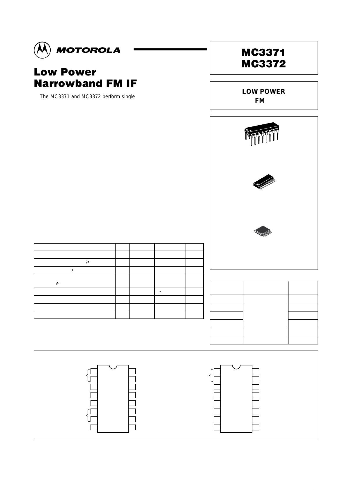
SO–16
TSSOP–16
D SUFFIX
PLASTIC PACKAGE
CASE 751B
(SO–16)
P SUFFIX
PLASTIC PACKAGE
CASE 648
MC3371P
MC3372DTB
Plastic DIP
TSSOP–16
Order this document by MC3371/D
MC3372P
Plastic DIP
16
1
16
1
DTB SUFFIX
PLASTIC PACKAGE
CASE 948F
(TSSOP–16)
16
1
MC3372D SO–16
ORDERING INFORMATION
1
MOTOROLA ANALOG IC DEVICE DATA
The MC3371 and MC3372 perform single conversion FM reception and
consist of an oscillator, mixer, limiting IF amplifier, quadrature discriminator,
active filter, squelch switch, and meter drive circuitry. These devices are
designed for use in FM dual conversion communication equipment. The
MC3371/MC3372 are similar to the MC3361/MC3357 FM IFs, except that a
signal strength indicator replaces the scan function controlling driver which is
in the MC3361/MC3357. The MC3371 is designed for the use of parallel LC
components, while the MC3372 is designed for use with either a 455 kHz
ceramic discriminator, or parallel LC components.
These devices also require fewer external parts than earlier products. The
MC3371 and MC3372 are available in dual–in–line and surface mount
packaging.
• Wide Operating Supply Voltage Range: V
CC
= 2.0 to 9.0 V
• Input Limiting Voltage Sensitivity of –3.0 dB
• Low Drain Current: I
CC
= 3.2 mA, @ VCC = 4.0 V, Squelch Off
• Minimal Drain Current Increase When Squelched
• Signal Strength Indicator: 60 dB Dynamic Range
• Mixer Operating Frequency Up to 100 MHz
• Fewer External Parts Required than Earlier Devices
MAXIMUM RATINGS
Rating Pin Symbol Value Unit
Power Supply Voltage 4 VCC(max) 10 Vdc
RF Input Voltage (VCC q 4.0 Vdc) 16 V16 1.0 Vrms
Detector Input Voltage 8 V8 1.0 Vpp
Squelch Input Voltage
(VCC q 4.0 Vdc)
12 V12 6.0 Vdc
Mute Function 14 V
14
–0.7 to 10 V
pk
Mute Sink Current 14 l14 50 mA
Junction Temperature – T
J
150 °C
Storage Temperature Range – T
stg
–65 to +150 °C
NOTES: 1.Devices should not be operated at these values. The “Recommended Operating
Conditions” table provides conditions for actual device operation.
2.ESD data available upon request.
8
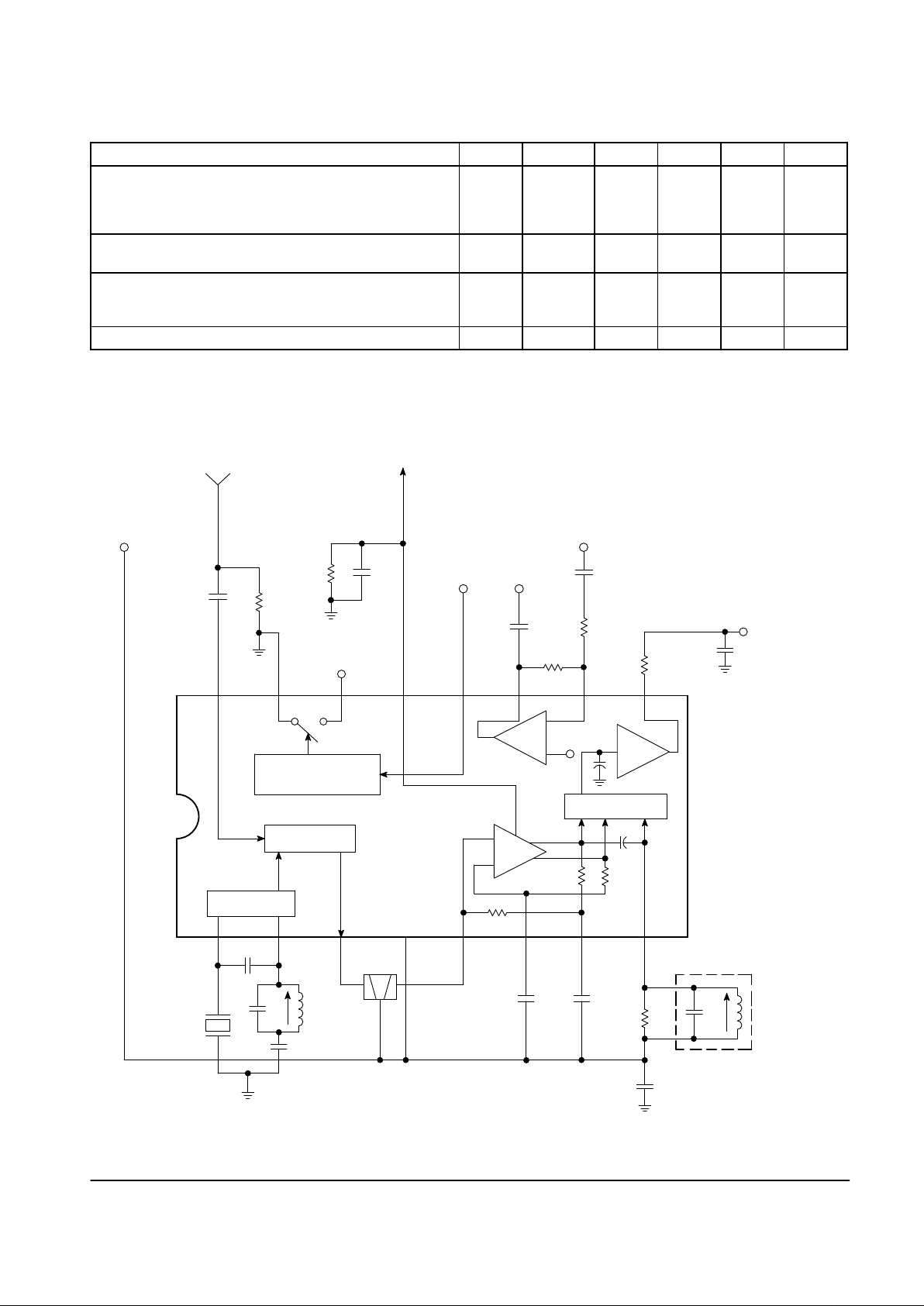
PIN CONNECTIONS
11
Gnd
Mute
Crystal Osc
Meter Drive
Squelch Input
Recovered Audio
Mixer Input
Filter Output
8
Mixer Output
Decoupling
Quad Coil
V
CC
MC3371
(Top View)
3
2
4
5
6
Limiter Input
10
7
16
1
15
14
13
12
9
Filter Input
Decoupling
Limiter Output
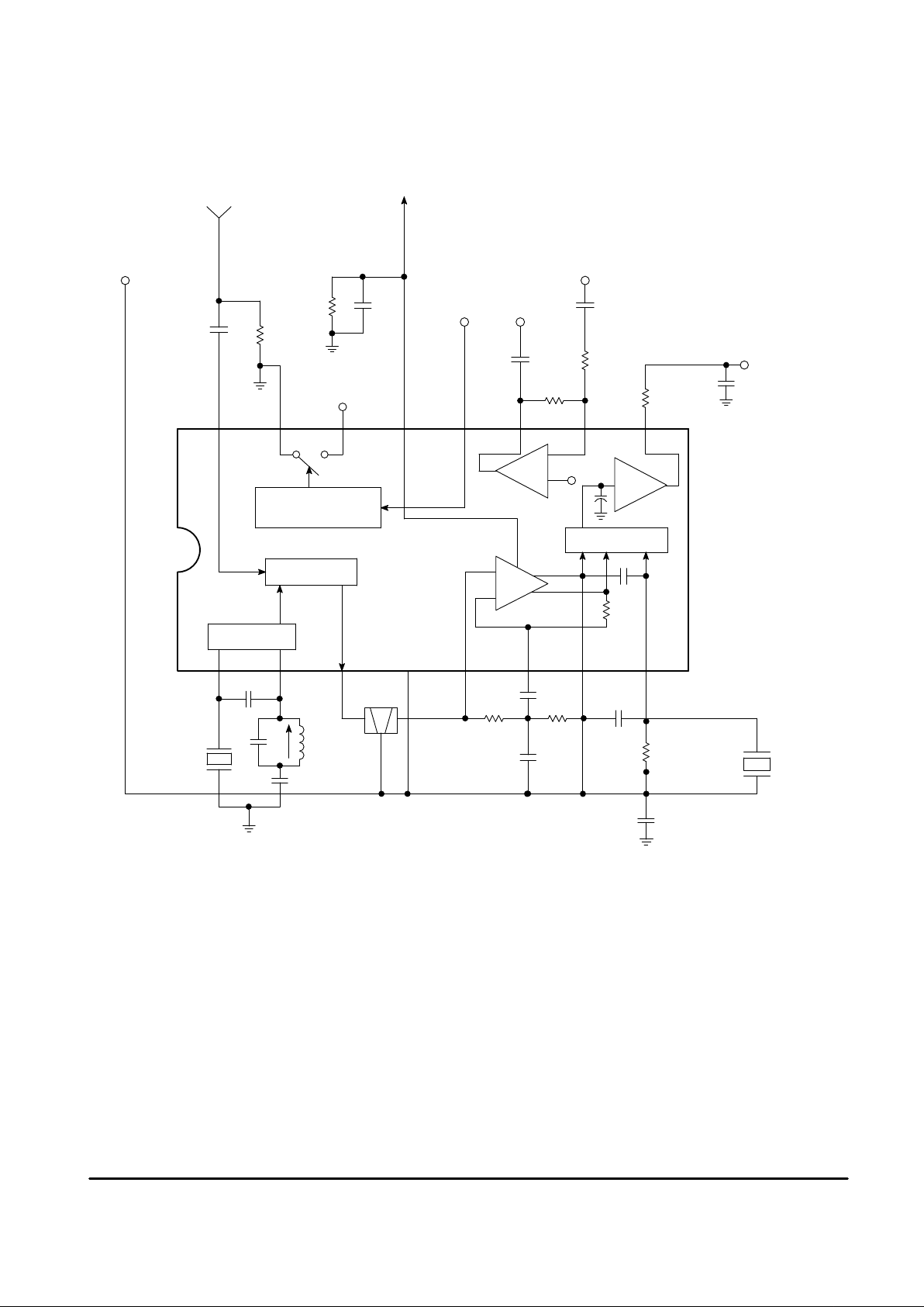
11
Gnd
Mute
Crystal Osc
Meter Drive
Squelch Input
Recovered Audio
Mixer Input
Filter Output
Mixer Output
Quad Input
V
CC
MC3372
(Top View)
3
2
4
5
6
Limiter Input
10
7
16
1
15
14
13
12
9
Filter Input
Motorola, Inc. 1996 Rev 1
MC3371 MC3372
2
MOTOROLA ANALOG IC DEVICE DATA
RECOMMENDED OPERATING CONDITIONS
Rating Pin Symbol Value Unit
Supply Voltage (@ TA = 25°C)
( –30°C p TA p +75°C)
4 V
CC
2.0 to 9.0
2.4 to 9.0
Vdc
RF Input Voltage 16 V
rf
0.0005 to 10 mVrms
RF Input Frequency 16 f
rf
0.1 to 100 MHz
Oscillator Input Voltage 1 V
local
80 to 400 mVrms
Intermediate Frequency – f
if
455 kHz
Limiter Amp Input Voltage 5 V
if
0 to 400 mVrms
Filter Amp Input Voltage 10 V
fa
0.1 to 300 mVrms
Squelch Input Voltage 12 V
sq
0 or 2 Vdc
Mute Sink Current 14 l
sq
0.1 to 30 mA
Ambient Temperature Range – T
A
–30 to +70 °C
AC ELECTRICAL CHARACTERISTICS (V
CC
= 4.0 Vdc, fo = 58.1125 MHz, df = ±3.0 kHz, f
mod
= 1.0 kHz, 50 Ω source,
f
local
= 57.6575 MHz, V
local
= 0 dBm, TA = 25°C, unless otherwise noted)
Characteristic
Pin Symbol Min Typ Max Unit
Input for 12 dB SINAD
Matched Input – (See Figures
11, 12 and 13)
Unmatched Input – (See Figures 1 and 2)
– V
SIN
–
–
1.0
5.0
–
15
µVrms
Input for 20 dB NQS – V
NQS
– 3.5 – µVrms
Recovered Audio Output Voltage
Vrf = –30 dBm
– AF
O
120 200 320
mVrms
Recovered Audio Drop Voltage Loss
Vrf = –30 dBm, VCC = 4.0 V to 2.0 V
– AF
loss
–8.0 –1.5 –
dB
Meter Drive Output Voltage (No Modulation)
Vrf = –100 dBm
Vrf = –70 dBm
Vrf = –40 dBm
13 M
Drv
MV1
MV2
MV3
–
1.1
2.0
0.3
1.5
2.5
0.5
1.9
3.1
Vdc
Filter Amp Gain
Rs = 600 Ω , fs = 10 kHz, Vfa = 1.0 mVrms
– A
V(Amp)
47 50 –
dB
Mixer Conversion Gain
Vrf = –40 dBm, RL = 1.8 kΩ
– A
V(Mix)
14 20 –
dB
Signal to Noise Ratio
Vrf = –30 dBm
– s/n
36 67 –
dB
Total Harmonic Distortion
Vrf = –30 dBm, BW = 400 Hz to 30 kHz
– THD
– 0.6 3.4
%
Detector Output Impedance 9 Z
O
– 450 – Ω
Detector Output Voltage (No Modulation)
Vrf = –30 dBm
9 DV
O
– 1.45 –
Vdc
Meter Drive
Vrf = –100 to –40 dBm
13 M
O
– 0.8 –
µA/dB
Meter Drive Dynamic Range
RF
In
IFIn (455 kHz)
13 MVD
–
–
60
80
–
–
dB
Mixer Third Order Input Intercept Point
f1 = 58.125 MHz
f2 = 58.1375 MHz
– ITO
Mix
– –22 –
dBm
Mixer Input Resistance 16 R
in
– 3.3 – kΩ
Mixer Input Capacitance 16 C
in
– 2.2 – pF
MC3371 MC3372
3
MOTOROLA ANALOG IC DEVICE DATA
DC ELECTRICAL CHARACTERISTICS (V
CC
= 4.0 Vdc, TA = 25°C, unless otherwise noted)
Characteristic Pin Symbol Min Typ Max Unit
Drain Current (No Input Signal)
Squelch Off, Vsq = 2.0 Vdc
Squelch On, Vsq = 0 Vdc
Squelch Off, VCC = 2.0 to 9.0 V
4
lcc1
lcc2
dlcc1
–
–
–
3.2
3.6
1.0
4.2
4.8
2.0
mA
Detector Output (No Input Signal)
DC Voltage, V8 = V
CC
9 V9
0.9 1.6 2.3
Vdc
Filter Output (No Input Signal)
DC Voltage
Voltage Change, VCC = 2.0 to 9.0 V
11
V11
dV11
1.5
2.0
2.5
5.0
3.5
8.0
Vdc
Trigger Hysteresis – Hys 34 57 80 mV
Quad Coil TOKO
2A6597 HK (10 mm)
or
7MC–8128Z (7 mm)
15
22
0.33
0.001
57.6575
MHz
Oscillator
0.1 0.1
20 k
0.1
muRata
CFU455D2
or
equivalent
14
C1
0.01
51
51 k
RF Input
VCC = 4.0 Vdc
13
2438
–
5671
15
+
16
Mute
0.1
12 11 10 9
Filter
Out
1.0
µ
F
Demodulator
AF
Amp
RSSI Output
510 k
Sq
In
Filter
In
470
8.2 k
0.01
AF Out
to Audio
Power Amp
53 k
10
Limiter
Amp
Filter
Amp
Mixer
Squelch Trigger
with Hysteresis
Figure 1. MC3371 Functional Block Diagram and Test Fixture Schematic
1.8 k
51 k
1.0 µF
MC3371 MC3372
4
MOTOROLA ANALOG IC DEVICE DATA
15
22
0.33
0.001
57.6575
MHz
Oscillator
C15
0.1
Ceramic
Resonator
muRata
CFU455D2
or
equivalent
14
C1
0.01
51
51 k
RF Input
VCC = 4.0 Vdc
13
2438
–
5671
15
+
16
Mute
0.1
12 11 10 9
Filter
Out
1.0
µ
F
Demodulator
AF
Amp
RSSI Output
510 k
Sq
In
Filter
In
470
8.2 k
0.01
AF Out
to Audio
Power Amp
53 k
Limiter
Amp
Filter
Amp
Mixer
Squelch Trigger
with Hysteresis
C14
27
R10
1.8 k
R11
51 k
C12
0.1
C13
0.1
R12
4.3 k
muRata
CDB455C16
Figure 2. MC3372 Functional Block Diagram and Test Fixture Schematic
1.0 µF
10
MC3371 MC3372
5
MOTOROLA ANALOG IC DEVICE DATA
Figure 3. Total Harmonic Distortion
versus Temperature
–55
0
125
20
TA, AMBIENT TEMPERATURE (°C)
5.0 25 45
30
–140
10
40
50
60
–10065–80 –40–120 –20 0–60 20
TA = –30°C
TA = 25°C
10585
70
5.0
0
1.0
4.0
3.0
2.0
–35 –15
TA = 75°C
TA = 75°C
TA = –30°C
VCC = 4.0 Vdc
fo = 10.7 MHz
RF INPUT (dBm)
THD, TOT AL HARMONIC DISTORTION (%)
RSSI OUT( A)
µ
Figure 4. RSSI versus RF Input
VCC = 4.0 Vdc
RF Input = –30 dBm
fo = 10.7 MHz
TYPICAL CURVES
(Unmatched Input)
RSSI OUTPUT( A)
µ
–30 dBm
45 6525–35 –15
–70 dBm
TA, AMBIENT TEMPERATURE (
°
C)
5.0 105–55 12585
VCC = 4.0 Vdc
fo = 10.7 MHz
–110 dBm
–20
–10
VCC = 4.0 Vdc
TA = 27
°
C
100 MHz
3rd Order Products
–50
–60
–40
–30
–70
– 20 0 10– 50 – 10– 30– 40– 70
RF INPUT (dBm)
– 60
0
100 MHz
Desired Products
MIXER OUTPUT (dBm)
30
18
60
TA = –30°C
TA = 25°C
fo = 10.7 MHz
RFin –40 dBm
1.8 k
Ω
Load
TA = 75°C
48
54
6.0
42
36
0
24
18
12
6.0
9.0
12
8.0 9.0
21
–5.0 dBm
0 dBm
10
–15 dBm
1.0
–20 dBm
–10 dBm
5.0 dBm
40
f, FREQUENCY (MHz)
30
20
0
10010 1000
107.06.05.03.0 4.0
VCC, SUPPLY VOLT AGE (V)
1.0 2.0
30
27
24
0
15
3.0
0
RSSI OUTPUT( A)
µ
MIXER GAIN (dB)
Figure 5. RSSI Output versus Temperature Figure 6. Mixer Output versus RF Input
Figure 7. Mixer Gain versus Supply Voltage Figure 8. Mixer Gain versus Frequency
VCC = 4.0 Vdc
TA = 27
°
C
RFin = –40 dBm
MC3371 MC3372
6
MOTOROLA ANALOG IC DEVICE DATA
MC3371 PIN FUNCTION DESCRIPTION
OPERATING CONDITIONS V
CC
= 4.0 Vdc, RFIn = 100 µV, f
mod
= 1.0 kHz, f
dev
= 3.0 kHz. MC3371 at fRF = 10.7 MHz (see Figure 11).
Pin
Symbol
Internal Equivalent
Circuit
Description Waveform
1 OSC1
OSC1
V
CC
1
15 k
The base of the Colpitts oscillator. Use
a high impedance and low capacitance
probe or a “sniffer” to view the wave–
form without altering the frequency.
Typical level is 450 mVpp.
2 OSC2
200
µ
A
2
OSC2
The emitter of the Colpitts oscillator.
Typical signal level is 200 mVpp. Note
that the signal is somewhat distorted
compared to that on Pin 1.
3 MX
Out
3
4
Mixer
Out
V
CC
Output of the Mixer. Riding on the
455 kHz is the RF carrier component.
The typical level is approximately
60 mVpp.
4 V
CC
100
µ
A
1.5 k
Supply Voltage –2.0 to 9.0 Vdc is the
operating range. VCC is decoupled to
ground.
5 IF
In
1.8 k
7
51 k
53 k
5
IF
In
6
DEC1
Input to the IF amplifier after passing
through the 455 kHz ceramic filter. The
signal is attenuated by the filter. The
typical level is approximately
50 mVpp.
6
7
DEC1
DEC2
DEC2
60
µ
A
IF Decoupling. External 0.1 µF
capacitors connected to VCC.
8 Quad
Coil
10
V
CC
8
Quad Coil
50
µ
A
Quadrature Tuning Coil. Composite
(not yet demodulated) 455 kHz IF
signal is present. The typical level is
500 mVpp.

MC3371 MC3372
7
MOTOROLA ANALOG IC DEVICE DATA
MC3371 PIN FUNCTION DESCRIPTION (continued)
OPERATING CONDITIONS
VCC = 4.0 Vdc, RFIn = 100 µV, f
mod
= 1.0 kHz, f
dev
= 3.0 kHz. MC3371 at fRF = 10.7 MHz (see Figure 11).
Pin WaveformDescription
Internal Equivalent
Circuit
Symbol
9 RA
200
V
CC
Recovered Audio. This is a composite
FM demodulated output having signal
and carrier component. The typical
level is 1.4 Vpp.
RA
Out
9
100
µ
A
The filtered recovered audio has the
carrier component removed and is
typically 800 mVpp.
10 Fil
In
V
CC
10
Filter
In
30
µ
A
Filter Amplifier Input
11 Fil
Out
11
V
CC
Filter
Out
240
µ
A
Filter Amplifier Output. The typical
signal level is 400 mVpp.
12 Sq
In
Sq
In
12
12
µ
A
Squelch Input. See discussion in
application text.

MC3371 MC3372
8
MOTOROLA ANALOG IC DEVICE DATA
MC3371 PIN FUNCTION DESCRIPTION (continued)
OPERATING CONDITIONS
VCC = 4.0 Vdc, RFIn = 100 µV, f
mod
= 1.0 kHz, f
dev
= 3.0 kHz. MC3371 at fRF = 10.7 MHz (see Figure 11).
Pin WaveformDescription
Internal Equivalent
Circuit
Symbol
13 RSSI
RSSI
Out
1.8 k
Bias
13
V
CC
RSSI Output. Referred to as the
Received Signal Strength Indicator or
RSSI. The chip sources up to 60 µA
over the linear 60 dB range. This pin
may be used many ways, such as:
AGC, meter drive and carrier triggered
squelch circuit.
14 MUTE
40 k
Mute or
Sq
Out
14
Mute Output. See discussion in
application text.
15 Gnd
Gnd
15
Ground. The ground area should be
continuous and unbroken. In a two–
sided layout, the component side has
the ground plane. In a one–sided
layout, the ground plane fills around
the traces on the circuit side of the
board and is not interrupted.
16 MIX
In
Mixer
In
V
CC
16
3.3 k
10 k
Mixer Input –
Series Input Impedance:
@ 10 MHz: 309 – j33 Ω
@ 45 MHz: 200 – j13 Ω
*Other pins are the same as pins in MC3371.

MC3371 MC3372
9
MOTOROLA ANALOG IC DEVICE DATA
MC3372 PIN FUNCTION DESCRIPTION
OPERATING CONDITIONS
VCC = 4.0 Vdc, RFIn = 100 µV, f
mod
= 1.0 kHz, f
dev
= 3.0 kHz. MC3372 at fRF = 45 MHz (see Figure 13).
Pin
Symbol
Internal Equivalent
Circuit
Description Waveform
5 IF
In
IF
In
5
53 k
6
IF Amplifier Input
6 DEC1
53 k
6
DEC
60 µA
IF Decoupling. External 0.1 µF
capacitors connected to VCC.
7 IF
Out
IF
Out
7
120
µ
A
V
CC
50
µ
A
IF Amplifier Output Signal level is
typically 300 mVpp.
8 Quad
In
Quad
In
8
50
µ
A
V
CC
10
Quadrature Detector Input. Signal
level is typically 150 mVpp.
9 RA
9200
RA
Out
V
CC
Recovered Audio. This is a composite
FM demodulated output having signal
and carrier components. Typical level
is 800 mVpp.
RA
Out
100 µA
The filtered recovered audio has the
carrier signal removed and is typically
500 mVpp.

MC3371 MC3372
10
MOTOROLA ANALOG IC DEVICE DATA
Figure 9. MC3371 Circuit Schematic
Figure 10. MC3372 Circuit Schematic
100
µ
A
IF
Out
8
Quad
In
4
V
CC
5
1.8 k
IF
In
DEC1
53 k
51 k
X
200
9
RA
Out
100
µ
A
Squelch Out
+
Filter
Out
Bias
12 Squelch In
11
Mixer
Out
3
Bias
X
Y
X
OSC1
200
µ
A
2
1
16
14
15
Gnd
10
Filter
In
–
Meter Out
13
OSC2
V
CC
4
Y
Y
i
DEC2
7
Mixer
In
6
X
100
µ
A
Squelch Out
+
Filter
Out
Bias
12 Squelch In
11
Mixer
Out
3
Bias
X
Y
X
OSC1
200
µ
A
2
1
16
14
15
Gnd
10
Filter
In
–
Meter Out
13
OSC2
V
CC
4
Mixer
In
8
Quad
In
4
V
CC
5
IF
In
DEC
53 k
X
200
9
RA
Out
100
µ
A
Y
Y
i
7
6
X
10
10

MC3371 MC3372
11
MOTOROLA ANALOG IC DEVICE DATA
CIRCUIT DESCRIPTION
The MC3371 and MC3372 are low power narrowband FM
receivers with an operating frequency of up to 60 MHz. Its low
voltage design provides low power drain, excellent
sensitivity, and good image rejection in narrowband voice
and data link applications.
This part combines a mixer, an IF (intermediate frequency)
limiter with a logarithmic response signal strength indicator, a
quadrature detector, an active filter and a squelch trigger
circuit. In a typical application, the mixer amplifier converts an
RF input signal to a 455 kHz IF signal. Passing through an
external bandpass filter, the IF signal is fed into a limiting
amplifier and detection circuit where the audio signal is
recovered. A conventional quadrature detector is used.
The absence of an input signal is indicated by the
presence of noise above the desired audio frequencies. This
“noise band” is monitored by an active filter and a detector. A
squelch switch is used to mute the audio when noise or a
tone is present. The input signal level is monitored by a meter
drive circuit which detects the amount of IF signal in the
limiting amplifier.
APPLICATIONS INFORMATION
The oscillator is an internally biased Colpitts type with the
collector, base, and emitter connections at Pins 4, 1 and 2
respectively. This oscillator can be run under crystal control.
For fundamental mode crystals use crystal characterized
parallel resonant for 32 pF load. For higher frequencies, use
3rd overtone series mode type crystals. The coil (L2) and
resistor RD (R13) are needed to ensure proper and stable
operation at the LO frequency (see Figure 13, 45 MHz
application circuit).
The mixer is doubly balanced to reduce spurious radiation.
Conversion gain stated in the AC Electrical Characteristics
table is typically 20 dB. This power gain measurement was
made under stable conditions using a 50 Ω source at the
input and an external load provided by a 455 kHz ceramic
filter at the mixer output which is connected to the VCC (Pin 4)
and IF input (Pin 5). The filter impedance closely matches the
1.8 kΩ internal load resistance at Pin 3 (mixer output). Since
the input impedance at Pin 16 is strongly influenced by a
3.3 kΩ internal biasing resistor and has a low capacitance,
the useful gain is actually much higher than shown by the
standard power gain measurement. The Smith Chart plot in
Figure 17 shows the measured mixer input impedance
versus input frequency with the mixer input matched to a
50 Ω source impedance at the given frequencies. In order to
assure stable operation under matched conditions, it is
necessary to provide a shunt resistor to ground. Figures 11,
12 and 13 show the input networks used to derive the mixer
input impedance data.
Following the mixer, a ceramic bandpass filter is
recommended for IF filtering (i.e. 455 kHz types having a
bandwidth of ±2.0 kHz to ±15 kHz with an input and output
impedance from 1.5 kΩ to 2.0 kΩ). The 6 stage limiting IF
amplifier has approximately 92 dB of gain. The MC3371 and
MC3372 are different in the limiter and quadrature detector
circuits. The MC3371 has a 1.8 kΩ and a 51 kΩ resistor
providing internal dc biasing and the output of the limiter is
internally connected, both directly and through a 10 pF
capacitor to the quadrature detector; whereas, in the
MC3372 these components are not provided internally . Thus,
in the MC3371, no external components are necessary to
match the 455 kHz ceramic filter, while in the MC3372,
external 1.8 kΩ and 51 kΩ biasing resistors are needed
between Pins 5 and 7, respectively (see Figures 12 and 13).
In the MC3371, a parallel LCR quadrature tank circuit is
connected externally from Pin 8 to VCC (similar to the
MC3361). In the MC3372, a quadrature capacitor is needed
externally from Pin 7 to Pin 8 and a parallel LC or a ceramic
discriminator with a damping resistor is also needed from
Pin 8 to VCC (similar to the MC3357). The above external
quadrature circuitry provides 90° phase shift at the IF center
frequency and enables recovered audio.
The damping resistor determines the peak separation of
the detector and is somewhat critical. As the resistor is
decreased, the separation and the bandwidth is increased
but the recovered audio is decreased. Receiver sensitivity is
dependent on the value of this resistor and the bandwidth of
the 455 kHz ceramic filter.
On the chip the composite recovered audio, consisting of
carrier component and modulating signal, is passed through
a low pass filter amplifier to reduce the carrier component
and then is fed to Pin 9 which has an output impedance of
450 Ω. The signal still requires further filtering to eliminate
the carrier component, deemphasis, volume control, and
further amplification before driving a loudspeaker. The
relative level of the composite recovered audio signal at Pin 9
should be considered for proper interaction with an audio
post amplifier and a given load element. The MC13060 is
recommended as a low power audio amplifier.
The meter output indicates the strength of the IF level and
the output current is proportional to the logarithm of the IF
input signal amplitude. A maximum source current of 60 µA is
available and can be used to drive a meter and to detect a
carrier presence. This is referred to as a Received Strength
Signal Indicator (RSSI). The output at Pin 13 provides a
current source. Thus, a resistor to ground yields a voltage
proportional to the input carrier signal level. The value of this
resistor is estimated by (VCC(Vdc) – 1.0 V)/60 µA; so for
VCC= 4.0 Vdc, the resistor is approximately 50 kΩ and
provides a maximum voltage swing of about 3.0 V.
A simple inverting op amp has an output at Pin 11 and the
inverting input at Pin 10. The noninverting input is connected
to 2.5 V. The op amp may be used as a noise triggered
squelch or as an active noise filter. The bandpass filter is
designed with external impedance elements to discriminate
between frequencies. With an external AM detector, the
filtered audio signal is checked for a tone signal or for the
presence of noise above the normal audio band. This
information is applied to Pin 12.

MC3371 MC3372
12
MOTOROLA ANALOG IC DEVICE DATA
An external positive bias to Pin 12 sets up the squelch
trigger circuit such that the audio mute (Pin 14) is open or
connected to ground. If Pin 12 is pulled down to 0.9 V or
below by the noise or tone detector, Pin 14 is internally
shorted to ground. There is about 57 mV of hyteresis at
Pin 12 to prevent jitter. Audio muting is accomplished by
connecting Pin 14 to the appropriate point in the audio path
between Pin 9 and an audio amplifier. The voltage at Pin 14
should not be lower than –0.7 V; this can be assured by
connecting Pin 14 to the point that has no dc component.
Another possible application of the squelch switch may
be as a carrier level triggered squelch circuit, similar to the
MC3362/MC3363 FM receivers. In this case the meter
output can be used directly to trigger the squelch switch
when the RF input at the input frequency falls below the
desired level. The level at which this occurs is determined
by the resistor placed between the meter drive output
(Pin 13) and ground (Pin 15).
Figure 11. Typical Application for MC3371 at 10.7 MHz
–
10
C7
0.022
VR1 (Squelch Control)
10 k
VR2
10 k
AF Out
to Audio
Power Amp
3.3 k
R8
C10
68
10.245
MHz
L1
TKANS9443HM
6.8
µH ±
6%
D1+1N5817
R5
R6
4.7 k
560
R7
R9
4.7 k
510 k
10
53 k
51 k
+
8.2
µ
H
L2
1st IF 10.7 MHz
from Input
Front End
+
T2: Toko
2A6597 HK (10 mm)
or
7MC–8128Z (7 mm)
VCC = 4.0 Vdc RSSI Output
R2
10 k
C8
0.22
R11
560
C9
10
R1
51 k
C1
0.01
C17
0.1
C3
0.1
C4
0.001
C5
0.001
C11
220
C13
0.1
R10
39 k
C14
0.1
14 131516 12
11
9
24385671
Oscillator
muRata
CFU455D2
or
equivalent
Demodulator
Filter
Mixer
Squelch Trigger
with Hysteresis
AF
Limiter
Amp
1.8 k
C12
0.1
C2
4.7
µ
F
C15
91
R3
100 k
R4
1.0 k
Amp
Amp

MC3371 MC3372
13
MOTOROLA ANALOG IC DEVICE DATA
Figure 12. Typical Application for MC3372 at 10.7 MHz
–
10
C7
0.022
VR1 (Squelch Control)
10 k
VR2
10 k
AF Out
to Audio
Power Amp
3.3 k
R8
C10
68
10.245
MHz
L1
TKANS9443HM
6.8
µH ±
6%
D1+1N5817
R5
R6
4.7 k
560
R7
R9
4.7 k
510 k
53 k
+
8.2
µ
H
L2
1st IF 10.7 MHz
from Input
Front End
+
VCC = 4.0 Vdc RSSI Output
R2
10 k
C8
0.22
R13
560
C9
10
R1
51 k
C1
0.01
C6
0.1
C3
0.1
C4
0.001
C5
C2
220
C14
14 131516 12
11
9
24385671
Oscillator
muRata
CFU455D2
or
equivalent
Demodulator
Filter
Mixer
Squelch Trigger
with Hysteresis
AF
Limiter
Amp
C15
0.1
R10
1.8k
R11
51 k
C12
0.1
C13
0.1
R12
4.3 k
27p
muRata
CDB455C16
C16
91
C2
4.7
µ
F
R4
1.0 k
Amp
Amp
0.001
10

MC3371 MC3372
14
MOTOROLA ANALOG IC DEVICE DATA
2.0
2.5
–20–40–60–80
3.5
3.0
1.5
1.0
0.5
0
–120 –100
RSSI OUTPUT (Vdc)
fRF = 10.7 MHz
VCC = 4.0 Vdc
Reference Figure 11
Figure 13. Typical Application for MC3372 at 45 MHz
Figure 14. RSSI Output versus RF Input Figure 15. RSSI Output versus RF Input
–
RSSI Output
to Meter (Triplett – 100 kV)
3.5
3.0
muRata
CDB455C16
RF INPUT (dBm)
1.5
1.0
0.5
0
–120 –100 –80 –60 –40
2.5
–20
2.0
C7
0.022
VR1 (Squelch Control)
10 k
VR2
10 k
AF Out
to Audio
Power Amp
3.3 k
R8
L1
0.245
µ
H
Coilcraft
150–07J08
D1+1N5817
R6
4.7 k
560
R7
R9
4.7 k
510 k
RF Input
45 MHz
+
VCC = 4.0 Vdc
R2
12 k
C8
0.22
C18
75
C9
10
R14
51 k
C1
0.01
C6
0.1
C3
0.1
C4
0.001
C5
C2
4.7
R3
100 k
R4
1.0 k
R5
R1
470
53 k
14 131516 12
11 10
9
24385671
Oscillator
Demodulator
Filter
Mixer
Squelch Trigger
with Hysteresis
AF
Limiter
Amp
C10
30
C16
0.01
C11
5.0
R10
1.8 k
R11
51 k
R12
4.3 k
C15
0.1
muRata
CFU455D2
or
equivalent
C13
0.1
C14
27
C12
0.1
R13
1.0 k
44.545
MHz
Coilcraft
143–13J12
L2
0.84
µ
H
C17
120
RSSI OUTPUT (Vdc)
+
0.001
Amp
Amp
fRF = 45 MHz
VCC = 4.0 Vdc
Reference Figure 13
10

MC3371 MC3372
15
MOTOROLA ANALOG IC DEVICE DATA
Figure 16. S + N, N, AMR versus Input
Figure 17. Mixer Input Impedance versus Frequency
+j10
–j500
–j250
–j150
–j100
–j50
–j25
–j10
+j250
+j25
+j50
+j500
+j150
VCC = 4.0 Vdc
RF Input = –40 dBm
+j100
0
10
150
500250
25 50
N
–60
–70 –10–30–50–90–110
10
0
–10
–130
–50
–40
–30
–20
* Reference Figures 11, 12 and 13
RF INPUT (dBm)
S + N
S + N 30% AM
10.7 MHz
45 MHz
S + N, N, AMR (dB)
100
fRF = 10.7 MHz
VCC = 4.0 V
TA = 25
°
C

MC3371 MC3372
16
MOTOROLA ANALOG IC DEVICE DATA
Figure 18. MC3371 PC Board Component View with Matched Input at 10.7 MHz
Figure 19. MC3371 PC Board Circuit or Solder Side as Viewed through Component Side
METER
OUT
J4
R1
C3
R9
D1
C
5
R5
R4
C17
R3
R6
VR1
V
CC
J3
VR2
R8
R7
C8
C7
C1
L2
C2
+
C15
INPUT IF
10.7 MHZ
J1
L1
MC3371
IF 10.7 MHZ
FRONT END
C14
BNC
J3
XTAL
10.245
MHZ
C10
C11
CFU
455D 2
VCC
C13
MC3371
R10
J2
T2
AF OUT
BNC
GND
CUT
.325
I
+
C9
V
CC
COMPONENT SIDE
R11
C16
C12
GND
R2
C4
Above PC Board is laid out for the circuit in Figure 11.
SOLDER SIDE
CUT
.325
I
CUT
.325
I

MC3371 MC3372
17
MOTOROLA ANALOG IC DEVICE DATA
Figure 20. MC3372P PC Board Component View with Matched Input at 10.7 MHz
Figure 21. MC3372P PC Board Circuit or Solder Side as Viewed through Component Side
CDB
455
C16
CFU455D2
INPUT IF
10.7 MHZ
C15
J3
C10
C11
VCC
AF OUT
GND
CUT
.325
+
C9
VCC
COMPONENT SIDE
C12
GND
CUT
.325
R10
R
1
1
C
1
3
METER
OUT
J4
R1
C3
R9
D1
R5
R4
C6
R3
R6
VR1
V
CC
J3
VR2
R8
R7
C8
C7
C1
C2
+
C16
J1
L1
MC3372
IF 10.7 MHZ
FRONT END
BNC
XTAL
10.245
MHZ
MC3372
R12
J2
BNC
R13
C17
R2
C4
CUT
.325
C
5
L2
C14
Above PC Board is laid out for the circuit in Figure 12.
SOLDER SIDE

MC3371 MC3372
18
MOTOROLA ANALOG IC DEVICE DATA
OUTLINE DIMENSIONS
D SUFFIX
PLASTIC PACKAGE
CASE 751B–05
(SO–16)
ISSUE J
P SUFFIX
PLASTIC PACKAGE
CASE 648–08
ISSUE R
NOTES:
1. DIMENSIONING AND TOLERANCING PER ANSI
Y14.5M, 1982.
2. CONTROLLING DIMENSION: INCH.
3. DIMENSION L TO CENTER OF LEADS WHEN
FORMED PARALLEL.
4. DIMENSION B DOES NOT INCLUDE MOLD FLASH.
5. ROUNDED CORNERS OPTIONAL.
–A–
B
F
C
S
H
G
D
J
L
M
16 PL
SEATING
18
916
K
PLANE
–T–
M
A
M
0.25 (0.010) T
DIM MIN MAX MIN MAX
MILLIMETERSINCHES
A 0.740 0.770 18.80 19.55
B 0.250 0.270 6.35 6.85
C 0.145 0.175 3.69 4.44
D 0.015 0.021 0.39 0.53
F 0.040 0.70 1.02 1.77
G 0.100 BSC 2.54 BSC
H 0.050 BSC 1.27 BSC
J 0.008 0.015 0.21 0.38
K 0.110 0.130 2.80 3.30
L 0.295 0.305 7.50 7.74
M 0 10 0 10
S 0.020 0.040 0.51 1.01
____
NOTES:
1. DIMENSIONING AND TOLERANCING PER ANSI
Y14.5M, 1982.
2. CONTROLLING DIMENSION: MILLIMETER.
3. DIMENSIONS A AND B DO NOT INCLUDE
MOLD PROTRUSION.
4. MAXIMUM MOLD PROTRUSION 0.15 (0.006)
PER SIDE.
5. DIMENSION D DOES NOT INCLUDE DAMBAR
PROTRUSION. ALLOWABLE DAMBAR
PROTRUSION SHALL BE 0.127 (0.005) TOTAL
IN EXCESS OF THE D DIMENSION AT
MAXIMUM MATERIAL CONDITION.
18
16 9
SEATING
PLANE
F
J
M
R
X 45
_
G
8 PLP
–B–
–A–
M
0.25 (0.010) B
S
–T–
D
K
C
16 PL
S
B
M
0.25 (0.010) A
S
T
DIM MIN MAX MIN MAX
INCHESMILLIMETERS
A 9.80 10.00 0.386 0.393
B 3.80 4.00 0.150 0.157
C 1.35 1.75 0.054 0.068
D 0.35 0.49 0.014 0.019
F 0.40 1.25 0.016 0.049
G 1.27 BSC 0.050 BSC
J 0.19 0.25 0.008 0.009
K 0.10 0.25 0.004 0.009
M 0 7 0 7
P 5.80 6.20 0.229 0.244
R 0.25 0.50 0.010 0.019
____

MC3371 MC3372
19
MOTOROLA ANALOG IC DEVICE DATA
OUTLINE DIMENSIONS
DTB SUFFIX
PLASTIC PACKAGE
CASE 948F–01
(TSSOP–16)
ISSUE O
DIM MIN MAX MIN MAX
INCHESMILLIMETERS
A 4.90 5.10 0.193 0.200
B 4.30 4.50 0.169 0.177
C ––– 1.20 ––– 0.047
D 0.05 0.15 0.002 0.006
F 0.50 0.75 0.020 0.030
G 0.65 BSC 0.026 BSC
H 0.18 0.28 0.007 0.011
J 0.09 0.20 0.004 0.008
J1 0.09 0.16 0.004 0.006
K 0.19 0.30 0.007 0.012
K1 0.19 0.25 0.007 0.010
L 6.40 BSC 0.252 BSC
M 0 8 0 8
NOTES:
1 DIMENSIONING AND TOLERANCING PER ANSI
Y14.5M, 1982.
2 CONTROLLING DIMENSION: MILLIMETER.
3 DIMENSION A DOES NOT INCLUDE MOLD FLASH.
PROTRUSIONS OR GATE BURRS. MOLD FLASH
OR GATE BURRS SHALL NOT EXCEED 0.15
(0.006) PER SIDE.
4 DIMENSION B DOES NOT INCLUDE INTERLEAD
FLASH OR PROTRUSION. INTERLEAD FLASH OR
PROTRUSION SHALL NOT EXCEED
0.25 (0.010) PER SIDE.
5 DIMENSION K DOES NOT INCLUDE DAMBAR
PROTRUSION. ALLOWABLE DAMBAR
PROTRUSION SHALL BE 0.08 (0.003) TOTAL IN
EXCESS OF THE K DIMENSION AT MAXIMUM
MATERIAL CONDITION.
6 TERMINAL NUMBERS ARE SHOWN FOR
REFERENCE ONLY.
7 DIMENSION A AND B ARE TO BE DETERMINED
AT DATUM PLANE –W–.
____
SECTION N–N
SEATING
PLANE
IDENT.
PIN 1
1
8
16
9
DETAIL E
J
J1
B
C
D
A
K
K1
H
G
DETAIL E
F
M
L
2X L/2
–U–
S
U0.15 (0.006) T
S
U0.15 (0.006) T
S
U
M
0.10 (0.004) V
S
T
0.10 (0.004)
–T–
–V–
–W–
0.25 (0.010)
16X REFK
N
N

MC3371 MC3372
20
MOTOROLA ANALOG IC DEVICE DATA
Motorola reserves the right to make changes without further notice to any products herein. Motorola makes no warranty , representation or guarantee regarding
the suitability of its products for any particular purpose, nor does Motorola assume any liability arising out of the application or use of any product or circuit, and
specifically disclaims any and all liability, including without limitation consequential or incidental damages. “T ypical” parameters which may be provided in Motorola
data sheets and/or specifications can and do vary in different applications and actual performance may vary over time. All operating parameters, including “Typicals”
must be validated for each customer application by customer’s technical experts. Motorola does not convey any license under its patent rights nor the rights of
others. Motorola products are not designed, intended, or authorized for use as components in systems intended for surgical implant into the body, or other
applications intended to support or sustain life, or for any other application in which the failure of the Motorola product could create a situation where personal injury
or death may occur. Should Buyer purchase or use Motorola products for any such unintended or unauthorized application, Buyer shall indemnify and hold Motorola
and its officers, employees, subsidiaries, affiliates, and distributors harmless against all claims, costs, damages, and expenses, and reasonable attorney fees
arising out of, directly or indirectly, any claim of personal injury or death associated with such unintended or unauthorized use, even if such claim alleges that
Motorola was negligent regarding the design or manufacture of the part. Motorola and are registered trademarks of Motorola, Inc. Motorola, Inc. is an Equal
Opportunity/Affirmative Action Employer.
Mfax is a trademark of Motorola, Inc.
How to reach us:
USA/EUROPE/ Locations Not Listed: Motorola Literature Distribution; JAPAN: Nippon Motorola Ltd.: SPD, Strategic Planning Office, 4–32–1,
P.O. Box 5405, Denver, Colorado 80217. 303–675–2140 or 1–800–441–2447 Nishi–Gotanda, Shinagawa–ku, Tokyo 141, Japan. 81–3–5487–8488
Mfax: RMFAX0@email.sps.mot.com – TOUCHTONE 602–244–6609 ASIA /PACIFIC: Motorola Semiconductors H.K. Ltd.; 8B Tai Ping Industrial Park,
– US & Canada ONLY 1–800–774–1848 51 Ting Kok Road, Ta i Po, N.T., Hong Kong. 852–26629298
INTERNET: http://motorola.com/sps
MC3371/D
◊
 Loading...