

Datasheet MC33461SQ-43CTR, MC33461SQ-45CTR, MC33461SQ-27CTR, MC33461SQ-28CTR, MC33461SQ-30CTR Datasheet (MOTOROLA)
...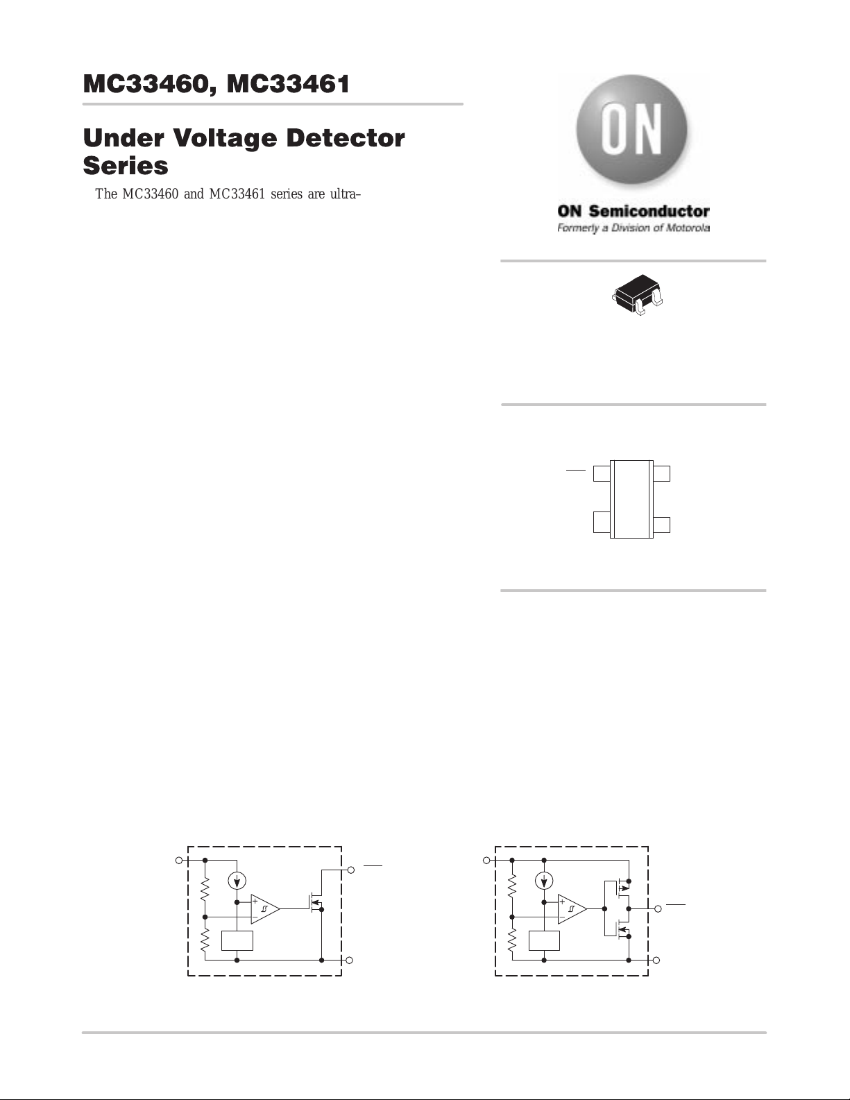
MC33460, MC33461
Under Voltage Detector
Series
The MC33460 and MC33461 series are ultra–low power CMOS
under–voltage detectors with very tight threshold accuracy
specifically designed for accurate monitoring of power supplies. The
devices are optimized for use in battery powered systems where low
quiescent current and small packaging are required. The device
generates an active–low signal whenever the input voltage falls below
the factory set ±2% threshold. Hysteresis is provided to ensure reliable
output switching.
The MC33460/1 series features a highly accurate voltage reference,
a comparator with a precision voltage threshold, and built–in
hysteresis to prevent erratic operation and a choice of output
configurations between Open Drain (MC33460) and complementary
push–pull (MC33461). The products are offered in 9 standard voltage
thresholds ranging from 0.9V to 4.5V. Other threshold voltages from
1.0 to 5.0V are available in 100mV steps. The devices can operate to a
very low input voltage level and are housed in the ultra–miniature
SC–82AB package.
Features
• Available in Open Drain or Push–Pull Output
• Output State Guaranteed to V
• Tight Detector Voltage Accuracy (±2.0%)
• Extended T emperature Operation (–40°C to 85°C)
• Ultra Low Quiescent Current (0.8 µA at V
• Wide Range of Operating Voltage (0.7 V to 10 V)
Applications
• Low Battery Detector
• Power–Fail Indicator
• Microprocessor Reset Generator
• Window Comparator
• Battery Backup Circuit
= 0.8 V
in
= 1.5 V typical)
in
http://onsemi.com
4
1
SC–82AB
SQ SUFFIX
CASE 419C
PIN CONNECTIONS
14
OUT
V
2
in
(Top View)
ORDERING INFORMATION
See detailed ordering and shipping information in the package
dimensions section on page 2 of this data sheet.
GND
3
N/C
Nch Open Drain Configuration
V
in
Semiconductor Components Industries, LLC, 1999
November, 1999 – Rev. 2
MC33460
V
ref
Representative Block Diagrams
V
OUT
GND
1 Publication Order Number:
in
MC33461
CMOS Configuration
V
ref
OUT
GND
MC33460/D
MC33460, MC33461
Nch
Oen
Drain
3000 Unit
h
Reel
CMOS
ORDERING INFORMATION
Threshold
Device
MC33460SQ–09ATR 0.9
MC33460SQ–20ATR 2.0 M0
MC33460SQ–27ATR 2.7
MC33460SQ–28ATR 2.8
MC33460SQ–30ATR 3.0
MC33460SQ–32ATR 3.2
MC33460SQ–43ATR 4.3 P3
MC33460SQ–45ATR 4.5 P5
MC33461SQ–09CTR 0.9
MC33461SQ–20CTR 2.0 V0
MC33461SQ–27CTR 2.7 V7
MC33461SQ–28CTR 2.8
MC33461SQ–30CTR 3.0
MC33461SQ–32CTR 3.2 W2
MC33461SQ–43CTR 4.3 X3
MC33461SQ–45CTR 4.5 X5
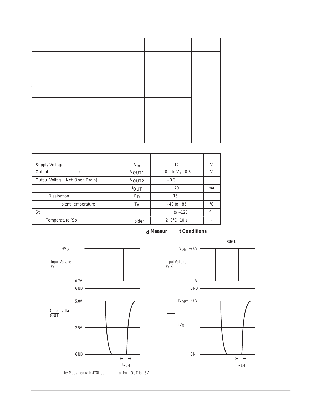
MAXIMUM RATINGS
Rating Symbol Value Unit
Supply Voltage
Output Voltage (CMOS)
Output Voltage (Nch Open Drain)
Output Current
Power Dissipation
Operating Ambient Temperature
Storage Temperature Range
Lead Temperature (Soldering)
Voltage
Type Marking
p
V
in
V
OUT1
V
OUT2
I
OUT
P
D
T
A
T
stg
T
solder
K9
M7
M8
N0
N2
T9
V8
W0
12
–0.3 to Vin+0.3
–0.3 to 12
70
150
–40 to +85
–40 to +125
260°C, 10 s
Package
(Qty/Reel)
s
on 7 inc
Reel
V
V
V
mA
mW
°C
°C
–
MC33460 MC33461
+V
+2.0V
DET
Input Voltage
(Vin)
0.7V
GND
5.0V
Output Voltage
(OUT
)
2.5V
GND
Note: Measured with 470k pullup resistor from OUT
Figure 1. Tpd Measurement Conditions
+V
+2.0V
DET
Input Voltage
(Vin)
0.7V
GND
+V
+2.0V
DET
Output Voltage
(OUT
)
+V
+2.0V
DET
2
GND
t
PLH
to +5V.
t
PLH
http://onsemi.com
2
MC33460, MC33461
Á
Á
Á
Á
Á
Á
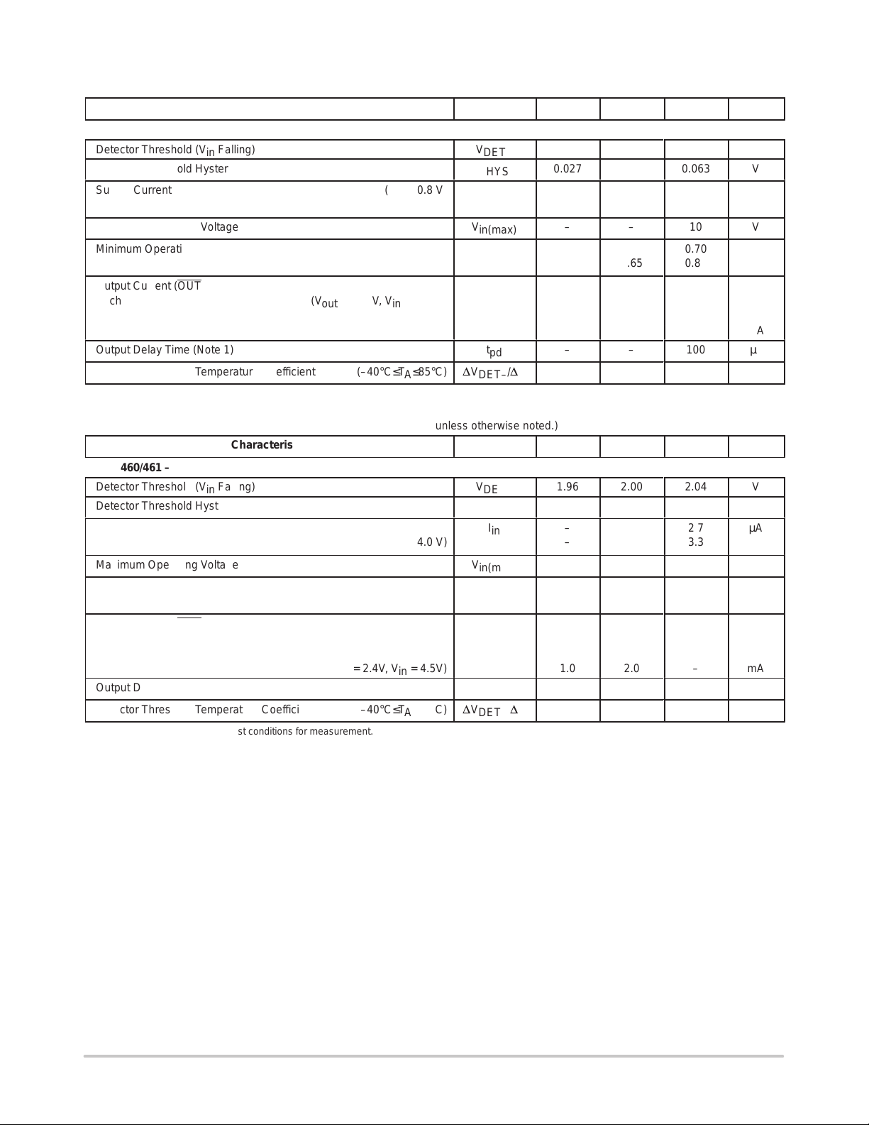
ELECTRICAL CHARACTERISTICS (For all values T
= 25°C, unless otherwise noted.)
A
Characteristic
MC33460/461 – 0.9
Detector Threshold (Vin Falling)
Detector Threshold Hysteresis V
Supply Current (Vin = 0.8 V)
(Vin = 2.9 V)
Maximum Operating Voltage V
Minimum Operating Voltage
(–40°C≤TA≤85°C)
Output Current (OUT)
Nch (V
CMOS Output High (V
= 0.05V, Vin = 0.70V) 0.01 0.05 – mA
out
(V
= 0.50V, Vin = 0.85V) 0.05 0.50 – mA
out
= 2.4V, Vin = 4.5V) 1.0 2.0 – mA
out
Output Delay Time (Note 1)
Detector Threshold Temperature Coefficient (–40°C≤TA≤85°C)
NOTES: 1.Refer to Figure 1 for test conditions for measurement.
ELECTRICAL CHARACTERISTICS (For all values T
= 25°C, unless otherwise noted.)
A
Characteristic
MC33460/461 – 2.0
Detector Threshold (Vin Falling)
Detector Threshold Hysteresis V
Supply Current (Vin = 1.9 V)
ББББББББББББББББ
(Vin = 4.0 V)
Maximum Operating Voltage V
Minimum Operating Voltage
(–40°C≤TA≤85°C)
Output Current (OUT)
Nch (V
CMOS Output High (V
= 0.05V, Vin = 0.70V) 0.01 0.05 – mA
out
(V
= 0.50V, Vin = 1.5V) 1.0 2.0 – mA
out
= 2.4V, Vin = 4.5V) 1.0 2.0 – mA
out
Output Delay Time (Note 1)
Detector Threshold Temperature Coefficient (–40°C≤TA≤85°C)
NOTES: 1.Refer to Figure 1 for test conditions for measurement.
Symbol Min Typ Max Unit
V
D
V
V
DET–
HYS
I
in
in(max)
in(min)
I
OUT
t
pd
DET–
/DT
0.882
0.900
0.918
0.027 0.045 0.063 V
–
–
0.8
1.0
2.4
3.0
– – 10 V
–
–
–
–
0.55
0.65
–
±100
0.70
0.80
100
–
Symbol Min Typ Max Unit
V
DET–
HYS
I
in
ÁÁÁ
in(max)
V
in(min)
I
OUT
t
pd
D
V
/DT
DET–
1.96
2.00
2.04
0.06 0.10 0.14 V
–
ÁÁ
–
0.9
ÁÁ
1.1
2.7
ÁÁ
3.3
– – 10 V
–
–
–
–
0.55
0.65
–
±100
0.70
0.80
100
–
V
µA
V
µs
PPM/°C
V
µA
Á
V
µs
PPM/°C
http://onsemi.com
3
MC33460, MC33461
Á
Á
Á
Á
Á
Á
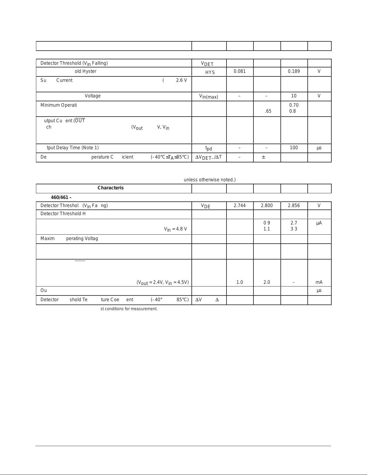
ELECTRICAL CHARACTERISTICS (For all values T
= 25°C, unless otherwise noted.)
A
Characteristic
MC33460/461 – 2.7
Detector Threshold (Vin Falling)
Detector Threshold Hysteresis V
Supply Current (Vin = 2.6 V)
(Vin = 4.7 V)
Maximum Operating Voltage V
Minimum Operating Voltage
(–40°C≤TA≤85°C)
Output Current (OUT)
Nch (V
CMOS Output High (V
= 0.05V, Vin = 0.70V) 0.01 0.05 – mA
out
(V
= 0.50V, Vin = 1.5V) 1.0 2.0 – mA
out
= 2.4V, Vin = 4.5V) 1.0 2.0 – mA
out
Output Delay Time (Note 1)
Detector Threshold Temperature Coefficient (–40°C≤TA≤85°C)
NOTES: 1.Refer to Figure 1 for test conditions for measurement.
ELECTRICAL CHARACTERISTICS (For all values T
= 25°C, unless otherwise noted.)
A
Characteristic
MC33460/461 – 2.8
Detector Threshold (Vin Falling)
Detector Threshold Hysteresis V
Supply Current (Vin = 2.7 V)
ББББББББББББББББ
(Vin = 4.8 V)
Maximum Operating Voltage V
Minimum Operating Voltage
(–40°C≤TA≤85°C)
Output Current (OUT)
Nch (V
CMOS Output High (V
= 0.05V, Vin = 0.70V) 0.01 0.05 – mA
out
(V
= 0.50V, Vin = 1.5V) 1.0 2.0 – mA
out
= 2.4V, Vin = 4.5V) 1.0 2.0 – mA
out
Output Delay Time (Note 1)
Detector Threshold Temperature Coefficient (–40°C≤TA≤85°C)
NOTES: 1.Refer to Figure 1 for test conditions for measurement.
Symbol Min Typ Max Unit
V
D
V
V
DET–
HYS
I
in
in(max)
in(min)
I
OUT
t
pd
DET–
/DT
2.646
2.700
2.754
0.081 0.135 0.189 V
–
–
0.9
1.1
2.7
3.3
– – 10 V
–
–
–
–
0.55
0.65
–
±100
0.70
0.80
100
–
Symbol Min Typ Max Unit
V
DET–
HYS
I
in
ÁÁÁ
in(max)
V
in(min)
I
OUT
t
pd
D
V
/DT
DET–
2.744
2.800
2.856
0.084 0.140 0.196 V
–
ÁÁ
–
0.9
ÁÁ
1.1
2.7
ÁÁ
3.3
– – 10 V
–
–
–
–
0.55
0.65
–
±100
0.70
0.80
100
–
V
µA
V
µs
PPM/°C
V
µA
Á
V
µs
PPM/°C
http://onsemi.com
4

MC33460, MC33461
Á
Á
Á
Á
Á
Á
ELECTRICAL CHARACTERISTICS (For all values T
= 25°C, unless otherwise noted.)
A
Characteristic
MC33460/461 – 3.0
Detector Threshold (Vin Falling)
Detector Threshold Hysteresis V
Supply Current (Vin = 2.87 V)
(Vin = 5.0 V)
Maximum Operating Voltage V
Minimum Operating Voltage
(–40°C≤TA≤85°C)
Output Current (OUT)
Nch (V
CMOS Output High (V
= 0.05V, Vin = 0.70V) 0.01 0.05 – mA
out
(V
= 0.50V, Vin = 1.5V) 1.0 2.0 – mA
out
= 2.4V, Vin = 4.5V) 1.0 2.0 – mA
out
Output Delay Time (Note 1)
Detector Threshold Temperature Coefficient (–40°C≤TA≤85°C)
NOTES: 1.Refer to Figure 1 for test conditions for measurement.
ELECTRICAL CHARACTERISTICS (For all values T
= 25°C, unless otherwise noted.)
A
Characteristic
MC33460/461 – 3.2
Detector Threshold (Vin Falling)
Detector Threshold Hysteresis V
Supply Current (Vin = 3.07 V)
ББББББББББББББББ
(Vin = 5.2 V)
Maximum Operating Voltage V
Minimum Operating Voltage
(–40°C≤TA≤85°C)
Output Current (OUT)
Nch (V
CMOS Output High (V
= 0.05V, Vin = 0.70V) 0.01 0.05 – mA
out
(V
= 0.50V, Vin = 1.5V) 1.0 2.0 – mA
out
= 2.4V, Vin = 4.5V) 1.0 2.0 – mA
out
Output Delay Time (Note 1)
Detector Threshold Temperature Coefficient (–40°C≤TA≤85°C)
NOTES: 1.Refer to Figure 1 for test conditions for measurement.
Symbol Min Typ Max Unit
V
D
V
V
DET–
HYS
I
in
in(max)
in(min)
I
OUT
t
pd
DET–
/DT
2.94
3.00
3.06
0.09 0.15 0.21 V
–
–
1.0
1.2
3.0
3.6
– – 10 V
–
–
–
–
0.55
0.65
–
±100
0.70
0.80
100
–
Symbol Min Typ Max Unit
V
DET–
HYS
I
in
ÁÁÁ
in(max)
V
in(min)
I
OUT
t
pd
D
V
/DT
DET–
3.136
3.200
3.264
0.096 0.160 0.224 V
–
ÁÁ
–
1.0
ÁÁ
1.2
3.0
ÁÁ
3.6
– – 10 V
–
–
–
–
0.55
0.65
–
±100
0.70
0.80
100
–
V
µA
V
µs
PPM/°C
V
µA
Á
V
µs
PPM/°C
http://onsemi.com
5

MC33460, MC33461
Á
Á
Á
Á
Á
Á
ELECTRICAL CHARACTERISTICS (For all values T
= 25°C, unless otherwise noted.)
A
Characteristic
MC33460/461 – 4.3
Detector Threshold (Vin Falling)
Detector Threshold Hysteresis V
Supply Current (Vin = 4.14 V)
(Vin = 6.3 V)
Maximum Operating Voltage V
Minimum Operating Voltage
(–40°C≤TA≤85°C)
Output Current (OUT)
Nch (V
CMOS Output High (V
= 0.05V, Vin = 0.70V) 0.01 0.05 – mA
out
(V
= 0.50V, Vin = 1.5V) 1.0 2.0 – mA
out
= 2.4V, Vin = 4.5V) 1.0 2.0 – mA
out
Output Delay Time (Note 1)
Detector Threshold Temperature Coefficient (–40°C≤TA≤85°C)
NOTES: 1.Refer to Figure 1 for test conditions for measurement.
ELECTRICAL CHARACTERISTICS (For all values T
= 25°C, unless otherwise noted.)
A
Characteristic
MC33460/461 – 4.5
Detector Threshold (Vin Falling)
Detector Threshold Hysteresis V
Supply Current (Vin = 4.34 V)
ББББББББББББББББ
(Vin = 6.5 V)
Maximum Operating Voltage V
Minimum Operating Voltage
(–40°C≤TA≤85°C)
Output Current (OUT)
Nch (V
CMOS Output High (V
= 0.05V, Vin = 0.70V) 0.01 0.05 – mA
out
(V
= 0.50V, Vin = 1.5V) 1.0 2.0 – mA
out
= 6.9V, Vin = 8.0V) 1.5 3.0 – mA
out
Output Delay Time (Note 1)
Detector Threshold Temperature Coefficient (–40°C≤TA≤85°C)
NOTES: 1.Refer to Figure 1 for test conditions for measurement.
Symbol Min Typ Max Unit
V
D
V
V
DET–
HYS
I
in
in(max)
in(min)
I
OUT
t
pd
DET–
/DT
4.214
4.300
4.386
0.129 0.215 0.301 V
–
–
1.1
1.3
3.3
3.9
– – 10 V
–
–
–
–
0.55
0.65
–
±100
0.70
0.80
100
–
Symbol Min Typ Max Unit
V
DET–
HYS
I
in
ÁÁÁ
in(max)
V
in(min)
I
OUT
t
pd
D
V
/DT
DET–
4.410
4.500
4.590
0.135 0.225 0.315 V
–
ÁÁ
–
1.1
ÁÁ
1.3
3.3
ÁÁ
3.3
– – 10 V
–
–
–
–
0.55
0.65
–
±100
0.70
0.80
100
–
V
µA
V
µs
PPM/°C
V
µA
Á
V
µs
PPM/°C
http://onsemi.com
6

MC33460, MC33461
TYPICAL CHARACTERISTICS
MC33461–0.9
2.5
TA = 85°C
µ
2.0
1.5
1.0
, SUPPLY CURRENT ( A)
in
I
0.5
0
0
2.0 4.0 6.0 8.0 10
INPUT VOLTAGE, Vin (V)
25°C
–40°C
MC33461–2.7
, DETECTOR THRESHOLD (V)
V
0.98
0.96
0.94
0.92
0.90
0.88
DET
0.86
0.84
1.0
V
V
HYS
–40 –20 0 20 100
–60
V
TEMPERATURE, TA (°C)
DET+(Vin
DET–(Vin
rising)
falling)
40 60 80
2.0
µ
1.5
1.0
, SUPPLY CURRENT ( A)
in
I
0.5
0
0
2.0 4.0 6.0 8.0 10
INPUT VOLTAGE, Vin (V)
TA = 85°C
25°C
–40°C
, DETECTOR THRESHOLD (V)
V
DET
2.9
2.8
2.7
2.6
2.5
V
V
HYS
–40 –20 0 20 10040 60 80
–60
V
TEMPERATURE, TA (°C)
DET+(Vin
DET–(Vin
rising)
falling)
MC33461–4.5
2.0
µ
1.5
1.0
, SUPPLY CURRENT ( A)
in
I
0.5
0
0
2.0 4.0 6.0 8.0 10
INPUT VOLTAGE, Vin (V)
TA = 85°C
25°C
–40°C
, DETECTOR THRESHOLD (V)
V
DET
4.8
4.7
4.6
4.5
4.4
V
V
HYS
V
–60
–40 –20 0 20 10040 60 80
TEMPERATURE, TA (°C)
DET+(Vin
DET–(Vin
rising)
falling)
Figure 2. Supply Current vs. Input Voltage
Figure 3. Detector Threshold Hysteresis vs. T emperature
http://onsemi.com
7

MC33460, MC33461
MC33461–0.9
m
, OUTPUT CURRENT ( A)
OUT
I
OUT
I , OUTPUT CURRENT (mA)
700
600
500
400
300
200
100
300
TA = 25°C
250
Vin = 0.85 V
TA = 25°C
0
0
0.2 0.4 0.80.6
V
, OUTPUT VOLTAGE (V)
OUT
m
OUT
I , OUTPUT CURRENT ( A)
200
150
100
Vin = 0.8 V
0.7 V0.7 V
50
0
0
0.02 0.04 0.10.06 0.08
V
, OUTPUT VOLTAGE (V)
OUT
MC33461–2.7
20
18
16
14
12
10
8
6
4
2
0
0
TA = 25°C
V
0.5 1.0
, OUTPUT VOLTAGE (V)
OUT
Vin = 2.5 V
2.0 V
1.5 V
m
OUT
I , OUTPUT CURRENT ( A)
300
250
200
150
100
TA = 25°C
Vin = 0.8 V
0.7 V
50
0
0
0.02 0.04 0.06 0.08 0.1
V
, OUTPUT VOLTAGE (V)
OUT
, OUTPUT CURRENT (mA)
OUT
I
MC33461–4.5
40
TA = 25°C
30
3.5 V
20
10
0
0
V
OUT
3.0 V
2.5 V
0.5 1
, OUTPUT VOLTAGE (V)
Vin = 4.5 V
4.0 V
2.0 V
1.5 V
Figure 4. Nch Output Current versus V
m
OUT
I , OUTPUT CURRENT ( A)
300
250
200
150
100
TA = 25°C
Vin = 0.8 V
0.7 V
50
0
0
0.02 0.04 0.10.06 0.08
V
, OUTPUT VOLTAGE (V)
OUT
in
http://onsemi.com
8

MC33460, MC33461
MC33461–2.7MC33461–0.9
m
, OUTPUT CURRENT ( A)
OUT
I
1.4
1.2
1.0
0.8
0.6
0.4
0.2
OUT
I , OUTPUT CURRENT (mA)
3.5
3.0
2.5
2.0
1.5
1.0
0.5
0
TA = 25°C
0
12 734
Vin, INPUT VOLTAGE (V)
V
OUT
= Vin – 2.1 V
1.5 V
1.0 V
0.5 V
56
TA = 25°C
V
= Vin – 0.7 V
OUT
0.5 V
0
0
24 86
Vin, INPUT VOLTAGE (V)
MC33461–4.5
4.5
OUT
I , OUTPUT CURRENT (mA)
4.0
3.5
3.0
2.5
2.0
1.5
1.0
0.5
0
TA = 25°C
V
= Vin – 2.1 V
OUT
1.5 V
1.0 V
0.5 V
0
210
468
Vin, INPUT VOLTAGE (V)
, OUTPUT VOLTAGE (V)
OUT
V
Figure 5. Output Current High versus Input Voltage
6
5
4
3
2
1
0
0
TA = –40°C
25°C
85°C
0.5 1 1.5 2 42.5 3 3.5
INPUT VOLTAGE, Vin (V)
Figure 6. T ypical Output Voltage versus Input Voltage
, OUTPUT VOLTAGE (V)
OUT
V
4.0
3.5
3.0
2.5
2.0
1.5
1.0
0.5
0.0
MC33461–2.7MC33460–2.7
85°C
25°C
TA = –40°C
0
0.5 1 1.5 2 42.5 3 3.5
INPUT VOLTAGE, Vin (V)
http://onsemi.com
9

MC33460, MC33461
MC33460–2.7MC33460–0.9
, OUTPUT DELAY TIME (ms)
P
t
0.001
100
1.0
0.1
0.01
10
0.0001
t
PLH
t
PHL
0.001 0.1
C
, LOAD CAPACITANCE (mF)
OUT
0.01
Figure 7. Output Delay Time versus Load Capacitance
K
L
J
Pin 1
, OUTPUT DELAY TIME (ms)
0.01
P
t
0.001
D
A
B
C
USER DIRECTION OF FEED
100
1.0
0.1
E
10
0.0001
t
PLH
t
PHL
0.001 0.1
C
, LOAD CAPACITANCE (mF)
OUT
A 2.2mm
F
G
H
B 2.6mm
C 4.0±0.1mm
D 4.0±0.1mm
E 2.0±0.05mm
F 1.75±0.1mm
G 3.5±0.05mm
H 8.0±0.3mm
J 1.5+0.1mm
K 0.2±0.1mm
L 1.6mm Max
0.01
178mm
21±0.8mm
Figure 8. T aping Specifications
2±0.5mm
Figure 9. Reel Dimensions
14.4mm MAX
13.0±0.2mm
60mm
8.4+2.0mm
http://onsemi.com
10

MC33460, MC33461
INFORMATION FOR USING THE SC–82AB SURFACE MOUNT PACKAGE
MINIMUM RECOMMENDED FOOTPRINT FOR SURFACE MOUNTED APPLICATIONS
Surface mount board layout is a critical portion of the total
design. The footprint for the semiconductor packages must
be the correct size to insure proper solder connection
0.60 0.60
0.80
0.60
0.80
SC–82AB
SOLDERING PRECAUTIONS
The melting temperature of solder is higher than the rated
temperature of the device. When the entire device is heated
to a high temperature, failure to complete soldering within
a short time could result in device failure. Therefore, the
following items should always be observed in order to
minimize the thermal stress to which the devices are
subjected.
• Always preheat the device.
• The delta temperature between the preheat and
soldering should be 100°C or less.*
• When preheating and soldering, the temperature of the
leads and the case must not exceed the maximum
temperature ratings as shown on the data sheet. When
using infrared heating with the reflow soldering
method, the difference shall be a maximum of 10°C.
interface between the board and the package. With the
correct pad geometry, the packages will self align when
subjected to a solder reflow process.
1.90
0.80
1.30
mm
• The soldering temperature and time shall not exceed
260°C for more than 10 seconds.
• When shifting from preheating to soldering, the
maximum temperature gradient shall be 5°C or less.
• After soldering has been completed, the device should
be allowed to cool naturally for at least three minutes.
Gradual cooling should be used as the use of forced
cooling will increase the temperature gradient and
result in latent failure due to mechanical stress.
• Mechanical stress or shock should not be applied
during cooling.
* Soldering a device without preheating can cause
excessive thermal shock and stress which can result in
damage to the device.
http://onsemi.com
11

MC33460, MC33461
PACKAGE DIMENSIONS
(SC–82AB)
SQ SUFFIX
PLASTIC PACKAGE
CASE 419C–01
ISSUE O
D3 PL
4
S
12
A
NOTES:
G
C
N
3
B
F
L
K
H
J
0.05 (0.002)
1. DIMENSIONING AND TOLERANCING PER ANSI
Y14.5M, 1982.
2. CONTROLLING DIMENSION: MILLIMETER.
DIM MIN MAX MIN MAX
A 1.8 2.2 0.071 0.087
B 1.15 1.45 0.045 0.057
C 0.8 1.1 0.031 0.043
D 0.2 0.4 0.008 0.016
F 0.3 0.5 0.012 0.020
G 1.1 1.5 0.043 0.059
H 0.0 0.1 0.000 0.004
J 0.10 0.26 0.004 0.010
K 0.1 ––– 0.004 –––
L 0.05 BSC 0.002 BSC
N 0.7 REF 0.028 REF
S 1.8 2.4 0.07 0.09
INCHESMILLIMETERS
ON Semiconductor and are trademarks of Semiconductor Components Industries, LLC (SCILLC). SCILLC reserves the right to make changes
without further notice to any products herein. SCILLC makes no warranty , representation or guarantee regarding the suitability of its products for any particular
purpose, nor does SCILLC assume any liability arising out of the application or use of any product or circuit, and specifically disclaims any and all liability ,
including without limitation special, consequential or incidental damages. “Typical” parameters which may be provided in SCILLC data sheets and/or
specifications can and do vary in different applications and actual performance may vary over time. All operating parameters, including “Typicals” must be
validated for each customer application by customer’s technical experts. SCILLC does not convey any license under its patent rights nor the rights of others.
SCILLC products are not designed, intended, or authorized for use as components in systems intended for surgical implant into the body, or other applications
intended to support or sustain life, or for any other application in which the failure of the SCILLC product could create a situation where personal injury or
death may occur. Should Buyer purchase or use SCILLC products for any such unintended or unauthorized application, Buyer shall indemnify and hold
SCILLC and its officers, employees, subsidiaries, affiliates, and distributors harmless against all claims, costs, damages, and expenses, and reasonable
attorney fees arising out of, directly or indirectly , any claim of personal injury or death associated with such unintended or unauthorized use, even if such claim
alleges that SCILLC was negligent regarding the design or manufacture of the part. SCILLC is an Equal Opportunity/Affirmative Action Employer .
PUBLICATION ORDERING INFORMATION
North America Literature Fulfillment:
Literature Distribution Center for ON Semiconductor
P.O. Box 5163, Denver, Colorado 80217 USA
Phone: 303–675–2175 or 800–344–3860 Toll Free USA/Canada
Fax: 303–675–2176 or 800–344–3867 Toll Free USA/Canada
Email: ONlit@hibbertco.com
N. American Technical Support: 800–282–9855 Toll Free USA/Canada
EUROPE: LDC for ON Semiconductor — European Support
German Phone: 303–308–7140 (Mon–Fri 2:30pm to 5:00pm Munich Time)
German Email: ONlit–german@hibbertco.com
French Phone: 303–308–7141 (Mon–Fri 2:30pm to 5:00pm T oulouse T ime)
French Email: ONlit–french@hibbertco.com
English Phone: 303–308–7142 (Mon–Fri 1:30pm to 5:00pm UK Time)
English Email: ONlit@hibbertco.com
http://onsemi.com
ASIA/PACIFIC: LDC for ON Semiconductor — Asia Support
Phone: 303–675–2121 (Tue–Fri 9:00am to 1:00pm, Hong Kong T ime)
T oll Free from Hong Kong 800–4422–3781
Email: ONlit–asia@hibbertco.com
JAPAN: ON Semiconductor, Japan Customer Focus Center
4–32–1 Nishi–Gotanda, Shinagawa–ku, T okyo, Japan 141–8549
Phone: 81–3–5487–8345
Email: r14153@onsemi.com
Fax Response Line: 303–675–2167
800–344–3810 Toll Free USA/Canada
ON Semiconductor Website: http://onsemi.com
For additional information, please contact your local Sales Representative.
MC33460/D
12
 Loading...