

Order this document by MC33364/D
The MC33364 series are variable frequency SMPS controllers that operate
in the critical conduction mode. They are optimized for low power, high density
power supplies requiring minimum board area, reduced component count,
and low power dissipation. Each narrow body SOIC package provides a small
footprint. Integration of the high voltage startup saves approximately 0.7 W of
power compared to resistor bootstrapped circuits.
Each MC33364 features an on–board reference, UVLO function, a
watchdog timer to initiate output switching, a zero current detector to ensure
critical conduction operation, a current sensing comparator, leading edge
blanking, and a CMOS driver. Protection features include the ability to shut
down switching, and cycle–by–cycle current limiting.
The MC33364D1 is available in a surface mount SO–8 package. It has an
internal 126 kHz frequency clamp. For loads which have a low power
operating condition, the frequency clamp limits the maximum operating
frequency , preventing excessive switching losses and EMI radiation.
The MC33364D2 is available in the SO–8 package without an internal
frequency clamp.
The MC33364D is available in the SO–16 package. It has an internal
126 kHz frequency clamp which is pinned out, so that the designer can
adjust the clamp frequency by connecting appropriate values of resistance.
• Lossless Off–Line Startup
• Leading Edge Blanking for Noise Immunity
• Watchdog T imer to Initiate Switching
• Minimum Number of Support Components
• Shutdown Capability
• Over Temperature Protection
• Optional Frequency Clamp
CRITICAL CONDUCTION
GREENLINE SMPS
CONTROLLER
SEMICONDUCTOR
TECHNICAL DATA
8
1
D1, D2 SUFFIX
PLASTIC PACKAGE
CASE 751
(SO–8)
16
1
D SUFFIX
PLASTIC PACKAGE
CASE 751B
(SO–16)
PIN CONNECTIONS
ORDERING INFORMATION
Operating
Device
MC33364D1
MC33364D2
MC33364D SO–16
Temperature Range
TJ = –25° to +125°C
Package
SO–8
SO–8
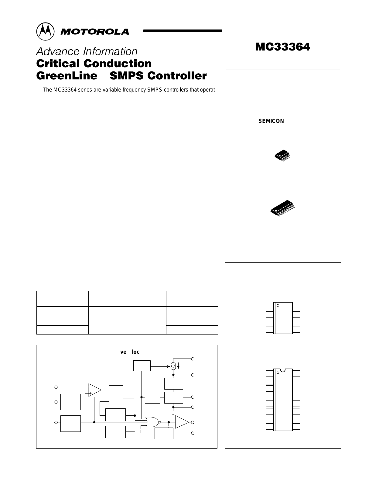
Representative Block Diagram
Restart
Delay
PWM
Comparator
FB
Current
Sense
ZC Det
This document contains information on a new product. Specifications and information herein
are subject to change without notice.
MOTOROLA ANALOG IC DEVICE DATA
Leading
Edge
Blanking
Zero
Current
Detector
This device contains 335 active transistors.
S
R
Q
R
Watchdog
Timer
Thermal
Shutdown
V
ref
UVLO
V
UVLO
Bandgap
Reference
Frequency
Clamp
CC
Line
V
CC
V
ref
Gnd
Gate
Optional
Frequency
Clamp
MC33364D1
MC33364D2
Zero Current
Current Sense
Voltage FB
Zero Current
Current Sense
Voltage FB
Freq Clamp
Motorola, Inc. 1997 Rev 0
18
2
3
V
4
ref
(Top View)
MC33364D
116
N/C
2
3
4
N/C
5
V
6
ref
7
N/C
8
(Top View)
Line
V
7
CC
Gate Drive
6
P Gnd
5
Line
A V
13
CC
P V
12
CC
11
Gate Drive
10
P Gnd
9
A Gnd
1
MAXIMUM RATINGS
Á
Á
Á
Á
Á
Á
Á
Á
Á
Á
Á
Á
ÁÁÁ
ÁÁÁ
ÁÁÁ
ÁÁÁ
ÁÁÁ
ÁÁÁ
ÁÁÁ
ÁÁÁ
Á
Á
Á
Á
Á
ÁÁÁ
Á
Á
Á
Á
Á
Á
ÁÁÁ
Á
Á
Á
Á
Á
Á
ÁÁÁ
Á
Á
Á
Á
Á
Á
ÁÁÁ
Á
ÁÁÁ
ÁÁÁ
ÁÁÁ
ÁÁÁ
ÁÁÁ
(TA = 25°C, unless otherwise noted.)
Rating Symbol Value Unit
Power Supply Voltage (Transient)
Power Supply Voltage (Operating)
Line Voltage
Current Sense, Compensation,
Voltage Feedback, Restart Delay and Zero
Current Input Voltage
Zero Current Detect Input
Restart Diode Current
Power Dissipation and Thermal Characteristics
D1 and D2 Suffix, Plastic Package Case 751
Maximum Power Dissipation @ TA = 70°C P
Thermal Resistance, Junction–to–Air R
D Suffix, Plastic Package Case 751B–05
Maximum Power Dissipation @ TA = 70°C P
Thermal Resistance, Junction–to–Air R
Operating Junction Temperature
ББББББББББББ
Operating Ambient Temperature
ББББББББББББ
Storage Temperature Range
ББББББББББББ
NOTE: ESD data available upon request.
V
CC
V
CC
V
Line
V
in1
I
in
I
in
D
θJA
D
θJA
T
J
ÁÁ
T
A
ÁÁ
T
stg
ÁÁ
MC33364
700
–1.0 to +10 V
±5.0
450 mW
178 °C/W
550 mW
145 °C/W
150
ÁÁÁ
–25 to +125
ÁÁÁ
–55 to +150
ÁÁÁ
20
16
5.0
mA
mA
°C
Á
°C
Á
°C
Á
V
V
V
ELECTRICAL CHARACTERISTICS (V
= 12 V, for typical values TA = 25°C, for min/max values TJ = –25 to 125°C)
CC
Characteristic
VOLTAGE REFERENCE
Reference Output Voltage (I
= 0 mA, TJ = 25°C)
Out
Line Regulation (VCC = 10 V to 20 V)
Load Regulation (I
Maximum V
ref
= 0 mA to 5.0 mA)
Out
Output Current
Reference Undervoltage Lockout Threshold
ZERO CURRENT DETECTOR
Input Threshold Voltage (Vin Increasing)
Hysteresis (Vin Decreasing)
Input Clamp Voltage
High State (I
Low State (I
= 3.0 mA) V
DET
= –3.0 mA) V
DET
CURRENT SENSE COMPARATOR
Input Bias Current (VCS = 0 to 2.0 V)
БББББББББББББББ
Built In Offset
БББББББББББББББ
Feedback Pin Input Range
БББББББББББББББ
Feedback Pin to Output Delay
БББББББББББББББ
DRIVE OUTPUT
БББББББББББББББ
Source Resistance (Drive = 0 V, V
Sink Resistance (Drive = VCC, V
= VCC – 1.0 V)
Gate
= 1.0 V) R
Gate
Output Voltage Rise T ime (25% – 75%) (CL = 1.0 nF)
Output Voltage Fall Time (75% – 25%) (CL = 1.0 nF)
Output Voltage in Undervoltage (VCC = 7.0 V, I
Sink
= 1.0 mA)
Symbol Min Typ Max Unit
V
ref
Reg
line
Reg
load
I
O
V
th
V
th
V
H
IH
IL
I
IB
ÁÁÁ
V
IO
ÁÁÁ
V
FB
ÁÁÁ
t
DLY
ÁÁÁ
ÁÁÁ
R
OH
OL
t
r
t
f
V
O(UV)
4.90
–
–
–
–
0.9
–
5.05
2.0
0.3
5
4.5
1.0
200
5.20
50
50
–
–
1.1
–
9.0 10.33 12
–0.5 –0.75 –1.1
–0.5
ÁÁÁ
50
ÁÁÁ
1.1
ÁÁÁ
100
ÁÁÁ
ÁÁÁ
10
0.02
ÁÁÁ
108
ÁÁÁ
1.24
ÁÁÁ
232
ÁÁÁ
ÁÁÁ
36
0.5
ÁÁ
170
ÁÁ
1.4
ÁÁ
400
ÁÁ
ÁÁ
70
5 11 25 Ω
–
–
–
67
28
0.01
150
50
0.03
ÁÁ
ÁÁ
ÁÁ
ÁÁ
ÁÁ
V
mV
mV
mA
V
V
mV
V
µA
mV
V
ns
Ω
ns
ns
V
2
MOTOROLA ANALOG IC DEVICE DATA
MC33364
ÁÁÁ
ÁÁÁ
ÁÁÁ
ÁÁÁ
ÁÁÁ
ÁÁÁ
Á
Á
Á
Á
Á
ÁÁÁ
Á
Á
Á
Á
Á
Á
ÁÁÁ
Á
ÁÁÁ
ÁÁÁ
ÁÁÁ
ÁÁÁ
ÁÁÁ
ÁÁÁ
ÁÁÁ
Á
Á
Á
Á
Á
ÁÁÁ
Á
ÁÁÁ
ELECTRICAL CHARACTERISTICS (continued) (V
= 12 V, for typical values TA = 25°C, for min/max values TJ = –25 to 125°C)
CC
Characteristic UnitMaxTypMinSymbol
LEADING EDGE BLANKING
Delay to Current Sense Comparator Input
(VFB = 2.0 V, VCS = 0 V to 4.0 V step, CL = 1.0 nF)
TIMER
Watchdog Timer
UNDERVOLTAGE LOCKOUT
Startup Threshold (VCC Increasing)
БББББББББББББББ
Minimum Operating Voltage After Turn–On (VCC Decreasing)
БББББББББББББББ
FREQUENCY CLAMP
БББББББББББББББ
Internal FC Function (pin open)
БББББББББББББББ
Internal FC Function (pin grounded)
БББББББББББББББ
Frequency Clamp Input Threshold
БББББББББББББББ
Frequency Clamp Control Current Range
БББББББББББББББ
TOTAL DEVICE
Line Startup Current (V
= 50 V) (VCC = V
Line
th(on)
– 1.0 V)
Restart Delay Time t
Line Pin Leakage (V
Line Startup Current (VCC = 0 V, V
= 575 V) I
Line
= 50 V) I
Line
VCC Dynamic Operating Current (50 kHz, CL = 1.0 nF)
VCC Static Operating Current (VCC = 16 V, V
БББББББББББББББ
ref
= 0)
VCC Pin Leakage (VCC = 11 V)
t
PHL(in/out)
t
DLY
V
th(on)
ÁÁÁ
V
Shutdown
ÁÁÁ
ÁÁÁ
f
max
ÁÁÁ
f
max
ÁÁÁ
V
th(FC)
ÁÁÁ
I
Control
ÁÁÁ
I
Line
DLY
Line
Line
I
CC
ÁÁÁ
ICC
Lkg
–
200
14
ÁÁÁ
6.5
ÁÁÁ
ÁÁÁ
ÁÁÁ90ÁÁÁ
400
ÁÁÁ
ÁÁÁ–ÁÁÁ
ÁÁÁ30ÁÁÁ70ÁÁ
5.0
250
410
15
ÁÁÁ
7.6
ÁÁÁ
ÁÁÁ
126
564
ÁÁÁ
2.0
8.5
700
16
ÁÁ
8.5
ÁÁ
ÁÁ
160
ÁÁ
700
ÁÁ
–
ÁÁ
110
12
100 ms
0.5 32 70 µA
6.0 10 12 mA
1.5
–
ÁÁÁ
300
2.75
3.0
ÁÁÁ
544
4.5
–
ÁÁ
800
ns
µs
V
ÁÁ
V
ÁÁ
ÁÁ
kHz
ÁÁ
kHz
ÁÁ
V
ÁÁ
µA
ÁÁ
mA
mA
ÁÁ
µA
MOTOROLA ANALOG IC DEVICE DATA
3
MC33364
0
5
OUTPUT VOLTAGE (V)
30
25
20
15
10
5.0
–5.0
16
12
8.0
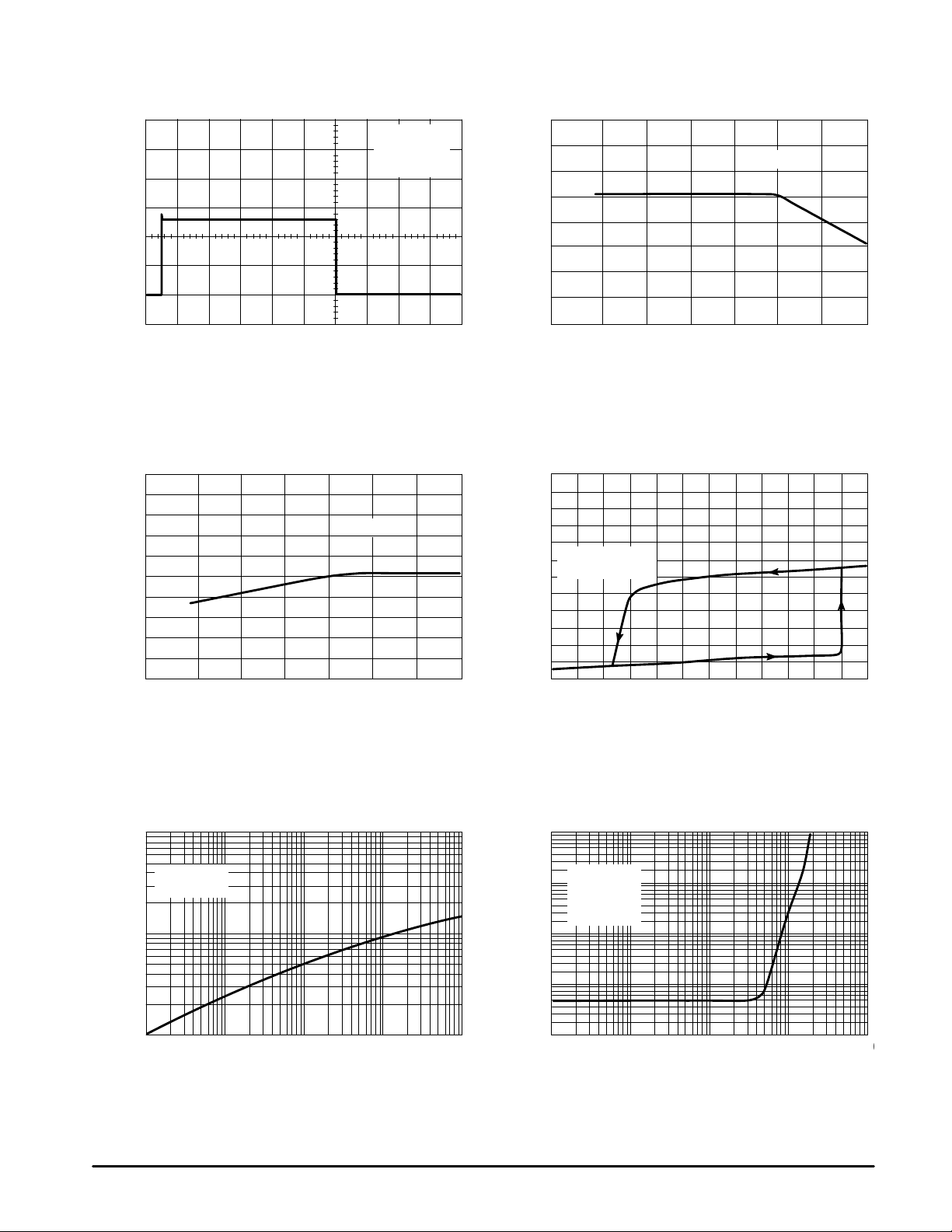
Figure 1. Drive Output Waveform
Figure 2. Watchdog Timer Delay
versus T emperature
VCC = 14 V
CL = 1000 pF
°
C
TA = 25
0
5.0 µs/DIV
Figure 3. Reference V oltage
versus T emperature
VCC = 14 V
µ
, WATCHDOG TIME DELAY ( s)
DLY
t
500
450
400
350
300
–55
6.0
4.0
Circuit of Figure 7
TA = 25
VCC = 14 V
–25 0 25 50 75 100 12
TA, AMBIENT TEMPERATURE (°C)
Figure 4. Supply Current
versus Supply V oltage
°
C
4.0
, VOLTAGE FEEDBACK
FB
V
THRESHOLD CHANGE (mV)
5.0
∆
–4.0
–55
–25 0 25 50 75 125100
TA, AMBIENT TEMPERATURE (°C)
Figure 5. Transient Thermal Resistance
1000
D Suffix
16 Pin SOIC
°
100
, THERMAL RESISTANCE
JA(t)
JUNCTION–TO–AIR ( C/W)
θ
R
10
0.01
0.1 1.0 10 100
t, TIME (s)
2.0
, SUPPLY CURRENT (mA)
CC
I
0
4.0
1000
µ
100
10
1.0
, PROGRAMMED DEAD TIME ( sec)
d
T
0.1
0.1
6.0 8.0 10 12 14 16
VCC, SUPPLY VOLTAGE (V)
Figure 6. Dead Time
versus Input Current
D Suffix
16 Pin SOIC
°
C
TA = 25
VCC = 14 V
1.0 10 100 100
Iin, CURRENT SOURCED INTO PIN 8 (µA)
4
MOTOROLA ANALOG IC DEVICE DATA
MC33364
FUNCTIONAL DESCRIPTION
INTRODUCTION
With the goal of reducing the size and cost of off–line
power supplies, there is an ever increasing demand for an
economical method of obtaining a regulated galvanically
isolated dc output voltage using a control which operates
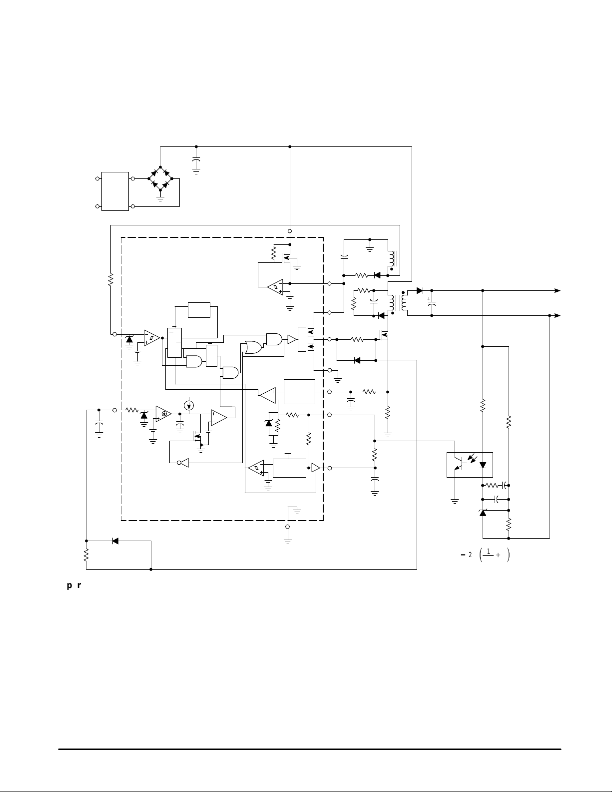
Figure 7. Functional Block Diagram
C5
10
D3
1N4006
92 to
270 Vac
EMI
Filter
1N4006
D2
D1
1N4006
1N4006
D4
MC33364
R2
22 k
1.5 V
UVLO
UVLO
+
Leading
Blanking
44 K
14 K
V
CC
5.0 V
Reference
Zero Current
Frequency
Clamp
C2
0.01
D9
1N4148
R13
100
4.0 K
10 V
Zero
Current
Detect
0.3/
0.25 V
2.0 V
RQ
Timer
R
Q
R
Q
S
En
5.0 V
10 pF
3.0
R
S
µ
Q
A
2.0 V
Line
+
15/7.6
Edge
5.0 k
A Gnd
directly from the ac line. This data sheet describes a
monolithic control IC that was specifically designed for power
supply control with a minimal number of external
components. It offers the designer a simple cost effective
solution to obtain the benefits of off–line power regulation.
T1
En
C3
V
CC
P V
Gate Drive
P Gnd
Current
Sense
Voltage FB
V
ref
1N4934
20
+
D5
CC
R1 56
R5 47 k
R6
47 K
470 R4
D7
1N4148
R12 100
C9 .01
C4
.001
R3
1.2 K
C10
0.1
D6
MURS160T3
Q1
MTD1N60
R7
2.2
D8
MBRS340T3
C5
300
U3
MOC8102
VO+
5
39 k
U2
TL431
2.5
R9
R8
430
R10
14 k
1
24
C7
10
2
R10
R11
C8
330 pF
1
R11
10 k
Ǔ
)
1
3
ǒ
6.0 V
2 Amp
Operating Description
The MC33364 contains many of the building blocks and
protection features that are employed in modern high
performance current mode power supply controllers.
Referring to the block diagram in Figure 7, note that this
device does not contain an oscillator. A description of each of
the functional blocks is given below.
Zero Current Detector
The MC33364 operates as a critical conduction current
mode controller, whereby output switch conduction is
initiated by the Zero Current Detector and terminated when
the peak inductor current reaches the input threshold level.
The Zero Current Detector initiates the next on–time by
MOTOROLA ANALOG IC DEVICE DATA
setting the RS Latch at the instant the inductor current
reaches zero. This critical conduction mode of operation has
two significant benefits. First, since the MOSFET cannot
turn–on until the inductor current reaches zero, the output
rectifier’s reverse recovery time becomes less critical
allowing the use of an inexpensive rectifier. Second, since
there are no deadtime gaps between cycles, the ac line
current is continuous thus limiting the peak switch to twice
the average input current
The Zero Current Detector indirectly senses the inductor
current by monitoring when the auxiliary winding voltage falls
below 0.25 V . To prevent false tripping, 50 mV of hysteresis is
provided. The Zero Current Detector input is internally
5

MC33364
protected by two clamps. The upper 0.7 V clamp prevents
input overvoltage breakdown while the lower –0.7 V clamp
prevents substrate injection. An external resistor must be
used in series with the auxiliary winding to limit the current
through the clamps to 5.0 mA or less.
Current Sense Comparator and RS Latch
The Current Sense Comparator RS Latch configuration
used ensures that only a single pulse appears at the Drive
Output during a given cycle. The inductor current is
converted to a voltage by inserting a ground–referenced
sense resistor in series with the source of output switch. This
voltage is monitored by the Current Sense Input and
compared to the divided down feedback voltage. The internal
feedback voltage divider is limited to 1.5 V maximum.
Therefore the maximum peak switch current is:
I
pk(max)
The Current Sense Input to Drive Output propagation
delay is typically 232 nS.
Timer
A watchdog timer function was added to the IC to eliminate
the need for an external oscillator when used in stand alone
applications. The Timer provides a means to automatically
start or restart the preconverter if the Drive Output has been
off for more than 410 microseconds after the inductor current
reaches zero.
Undervoltage Lockout
The MC33364 has a 5.0 V internal reference brought out
to Pin 6 (D Suffix) or Pin 4 (D1 and D2 Suffixes) and capable
of sourcing 10 mA typically . It also contains an Under V oltage
Lockout (UVLO) circuit which suppresses the Gate output at
Pin 1 1 if the VCC supply voltage drops below 7.6 V typical.
Restart Delay
A restart delay function is provided to allow hiccup mode
fault protection in case of a short circuit condition and to
prevent the SMPS from repeatedly trying to restart after the
input line voltage has been removed. When power is first
applied, the VCC bypass capacitor is charged through a
constant current source. The Restart Delay turns off the high
voltage startup MOSFET when VCC reaches the startup
threshold level. The Restart Delay turns on the high voltage
MOSFET after VCC has dropped below 4.5 V.
If the SMPS output is short circuited, the transformer
winding, which provides the VCC voltage to the MC33364, will
be unable to sustain VCC. The restart delay prevents the high
voltage startup transistor within the IC from maintaining the
voltage on the VCC pin bootstrap capacitor. After VCC drops
below the UVLO threshold in the SMPS, the SMPS switching
transistors are held off for the time programmed by the restart
delay circuit. In this manner, the SMPS switching transistor is
operated at a very low duty cyle, preventing destruction. If
the short circuit fault is removed, the power supply system
will turn on by itself in a normal startup mode after the restart
delay has timed out
+
1.5 V
R
Sense
Figure 8. Frequency Clamp Circuit
5.0 V
µ
A
10 pF
3.0
0 = Disable
FC Output
to PWM latch
2.0 V
Frequency
Clamp
4.0 k
2.0 V
Gate
Drive
Signal
Output Switching Frequency Clamp
In normal operation, the MC33364 operates the flyback
transformer primary inductance in the critical mode. That is,
the inductor current ramps to a peak value, ramps down to
zero, then immediately begins ramping positive again. The
peak current is programmed by the current sense resistance
value. If the output load is reduced from full load to a standby
load or no load condition, the switching frequency can
increase to hundreds of kilohertz. Because regulatory
agency EMI limits for allowed conducted current decreases
as the switching frequency increases beyond 150 kHz, this
may be an undesireable operating condition. The Output
Switching Frequency Clamp remedies this situation to
minimize EMI generated in this operating region. The internal
frequency clamp circuit in the MC33364D1 and MC33364D
programs a minimum off time, forcing discontinuous mode
operation and limiting the operating frequency to less than
126 kHz. The MC33364D2 does NOT contain a frequency
clamp circuit. The Output Switching Frequency Clamp
function in the MC33364D can be disabled by connecting the
FC input, Pin 8, to ground. The clamp frequency can be set
externally by sinking or sourcing a current into the pin of up to
100 microamperes.
Output
The IC contains a CMOS output driver specifically
designed for direct drive of power MOSFETs. The Drive
Output is capable of up to ±1500 mA peak current with a
typical rise and fall time of 50 nS with a 1.0 nF load. Additional
internal circuitry has been added to keep the Drive Output in
a sinking mode whenever the Undervoltage Lockout is
active. This characteristic eliminates the need for an external
gate pull–down resistor. The totem–pole output has been
optimized to minimize cross–conduction current during high
speed operation.
Design Example
Design an off–line Flyback converter according to the
following requirements:
Output Power: 12 W
Output: 6.0 V @ 2 Amperes
Input voltage range: 90 Vac – 270 Vac, 50/60 Hz
The operation for the circuit shown in Figure 9 is as
follows: the rectifier bridge D1–D4 and the capacitor C1
convert the ac line voltage to dc. This voltage supplies the
primary winding of the transformer T1 and the startup circuit
6
MOTOROLA ANALOG IC DEVICE DATA

MC33364
in U1 through Pin 8. The primary current loop is closed by the
transformer’s primary winding, the TMOS switch Q1 and the
current sense resistor R7. The switch Q1 is driven from Pin 6
of U1 through the resistor R4 and the diode D7. The resistor
R4 smooths the switch–on of Q1. The diode D7 ensures a
fast switching–off. The resistors R5, R6, diode D6 and
capacitor C4 create a clamping network that protects Q1
from spikes on the primary winding. The network consisting
of capacitor C3, diode D5 and resistor R1 provides a V
supply voltage for U1 from the auxiliary winding of the
transformer. The resistor R1 makes VCC more stable and
resistant to noise. The resistor R2 reduces the current flow
through the internal clamping and protection zener diode of
the Zero Crossing Detector (ZCD) within U1. C3 is the
decoupling capacitor of the supply voltage. The resistor R3
provides bias current for the optoisolator’s transistor. The
diode D8 and the capacitor C5 rectify and filter the output
voltage. The device U2 drives the primary side through the
optoisolator to make the output voltage stable. The output
voltage information is delivered to U2 by a resistive divider
that consists of resistors R10 and R11. The resistor R9 and
the capacitors C7, C8 provide frequency compensation of the
feedback loop.
Since the critical conduction mode converter is a variable
frequency system, the MC33364 has a built–in special block
to reduce switching frequency in the no load condition. This
block is named the ”frequency clamp” block. MC33364 used
in the design example has an internal frequency clamp set to
126 kHz. However, optional versions with a disabled or
variable frequency clamp are available. The frequency clamp
works as follows: the clamp controls the part of the switching
cycle when the MOSFET switch is turned off. If this ”off–time”
(determined by the reset time of the transformer’s core) is too
short, then the frequency clamp does not allow the switch to
turn–on again until the defined frequency clamp time is
reached (i.e., the frequency clamp will insert a dead time).
There are several advantages of the MC33364’s startup
circuit. The startup circuit includes a special high voltage
switch that controls the path between the rectified line
voltage and the VCC supply capacitor to charge that capacitor
by a limited current when the power is applied to the input.
After a few switching cycles the IC is supplied from the
transformer’s auxiliary winding. After VCC reaches the
undervoltage lockout threshold value, the startup switch is
turned off by the undervoltage and the overvoltage control
circuit. Because the power supply can be shorted on the
output, causing the auxiliary voltage to be zero, the MC33364
will periodically start its startup block. This mode is named
”hiccup mode”. During this mode the temperature of the chip
rises but remains protected by the thermal shutdown block.
During the power supply’s normal operation, the high voltage
internal MOSFET is turned off, preventing wasted power , and
thereby , allowing greater circuit efficiency.
Since a bridge rectifier is used, the resulting minimum and
maximum dc input voltages can be calculated:
V
in(min)
V
in(max)
Ǹ
dc+2
Ǹ
dc+2
xV
xV
in(min)
in(max)
ac
ac
Ǹ
+ǒ2
Ǹ
+ǒ2
Ǔ
(
90 Vac)+
Ǔ
(
270 Vac)+
CC
127 V
382 V
The maximum average input current is:
P
Iin+
where n = estimated circuit efficiency.
A TMOS switch with 600 V avalanche breakdown voltage
is used. The voltage on the switch’s drain consists of the
input voltage and the flyback voltage of the transformer’s
primary winding. There is a ringing on the rising edge’s top of
the flyback voltage due to the leakage inductance of the
transformer. This ringing is clamped by the RCD network.
Design this clamped wave for an amplitude of 50 V. Add
another 50 V to allow a safety margin for the MOSFET. Then
a suitable value of the flyback voltage may be calculated:
V
flbk
Since this value is very close to the V
V
flbk
The V
ē
max
The maximum input primary peak current:
I
ppk
Choose the desired minimum frequency f
to be 70 kHz.
After reviewing the core sizing information provided by a
core manufacturer, a EE core of size about 20 mm was
chosen. Siemens’ N67 magnetic material is used, which
corresponds to a Philips 3C85 or TDK PC40 material.
The primary inductance value is given by:
Lp+
The manufacturer recommends for that magnetic core a
maximum operating flux density of:
B
max
The cross–sectional area Ac of the EF20 core is:
Ac+
The operating flux density is given by:
B
max
From this equation the number of turns of the primary
winding can be derived:
np+
out
ƪ
nV
+
600 V*382 V*100 V+118 V
+
flbk
+
V
2I
+
[
ē
ē
max V
ǒ
I
ppk
+
33.5 mm
+
LpI
B
maxAc
ƫ
in(min)
V
TMOS
V
in(min)
value of the duty cycle is given by:
V
flbk
)
flbk
in
+
]
max
in(min)
ǒ
Ǔ
f
min
0.2 T
2
LpI
ppk
NpA
c
ppk
12 W
+
[
0.8(127 V
*
V
in(max)
+
127 V
V
in(min)
0.2(0.118 A
+
0.5
+
(
0.472 A)(70 kHz
Ǔ
+
0.118 A
)]
*
100 V
in(min)
127 V
[
127 V)127 V
)
+
0.472 A
0.5(127 V
)
+
, set:
+
]
of operation
min
+
1.92 mH
)
0.5
MOTOROLA ANALOG IC DEVICE DATA
7

MC33364
The AL factor is determined by:
ǒ
L
L
AL+
core with an AL of 100 nH is selected. The desired number of
turns of the primary winding is:
np+
(assuming a Schottky rectifier is used):
ns+
p
n2p
From the manufacturer‘s catalogue recommendation the
L
p
ǒ
Ǔ
A
L
The number of turns needed by the 6.0 V secondary is
ǒ
Vs)
ƪ
The auxiliary winding to power the control IC is 16 V and its
number of turns is given by:
naux
C1
where the minimum ripple frequency is 2 times the 50 Hz line
frequency and t
haversine cycle, is assumed to be half the cycle period.
calculations for the value of the output filter capacitors will be
done at the lowest frequency, since the ripple voltage will be
greatest at this frequency. The approximate equation for the
output capacitance value is given by:
C5
one uses the peak current in the predesign consideration.
Since within the IC there is a limitation of the voltage for the
current sensing, which is set to 1.2 V, the design of the
current sense resistor is simply given by:
R7
secondary, connected to the primary side via an optoisolator,
the MOC8102.
(V
+
The approximate value of rectifier capacitance needed is:
t
(Iin)
off
+
V
ripple
Because we have a variable frequency system, all the
I
+
(f
min
Determining the value of the current sense resistor (R7),
V
cs
+
I
ppk
The error amplifier function is provided by a TL431 on the
B
p
maxAc
+
ǒ
L
ƪ
p
ǒ
+
1ń2
ƪ
+
ǒ
Ǔ
V
1–ēmaxǓn
fwd
ē
maxǒV
in(min)
ǒ
+
)
V
aux
ƪ
ē
max(V
(16 V)0.9 V)(1*0.5)139
+
(5 m sec)(0.118 A)
+
, the discharge time of C1 during the
off
out
+
)(V
)
rip
1.2 V
+
0.472 A
2
Ǔ
2
Ǔ
I
ƫ
ppk
ǒ
Ǔ
0.2 T
33.5 E–6 m
ǒ
.00192 H
(
0.00192 H
(
6.0 V)0.3 V
fwd
(70 kHz)(0.1 V)
Ǔ
(
0.472 A
)
ƫ
100 nH
+
)
p
Ǔ
ƫ
ƪ
0.5ǒ127 V
)(1*ēmax)n
ƫ
)
in(min)
[0.5(127 V)]
50 V
2A
2.54W[
2
2
Ǔ
2
)
1ń2
+
139 turns
ǒ
Ǔ
1*0.5Ǔ139
Ǔ
ƫ
p
+
11.8mF
+
286mF
2.2
W
+
105 nH
+
7 turns
+
19 turns
The voltage of the optoisolator collector node sets the
peak current flowing through the power switch during each
cycle. This pin will be connected to the feedback pin of the
MC33364, which will directly set the peak current.
Starting on the secondary side of the power supply , assign
the sense current through the voltage–sensing resistor
divider to be approximately 0.25 mA. One can immediately
calculate the value of the lower and upper resistor:
V
(TL431)
R
R
current through the optoisolator and the TL431 is set by the
minimum operating current requirements of the TL431. This
currernt is minimum 1.0 mA. Assign the maximum current
through the branch to be 5 mA. That makes the bias resistor
value equal to:
R
100% with 25% tolerance. When the TL431 is full–on, 5 mA
will be drawn from the transistor within the MOC8102. The
transistor should be in saturated state at that time, so its
collector resistor must be
R
reference voltage to the feedback pin of the MC33364, the
external resistor can have a higher value
R
the optoisolator diode and the voltage sense divider on the
secondary side.
R
fpn+
+
lower
upper
The value of the resistor that would provide the bias
bias
The MOC8102 has a typical current transfer ratio (CTR) of
collector
Since a resistor of 5.0 k is internally connected from the
ext
This completes the design of the voltage feedback circuit.
In no load condition there is only a current flowing through
The load at that condition is given by:
noload
The output filter pole at no load is:
R11
+
R10
+
RS+
+
+
+R3+
+
(I
(2pR
ref
+
6.0 V*[2.5V)1.4V]
V
ref
(R
LED
noload
+
V
(R
I
int
V
1
I
div
V
*
V
out
out
*
LED
int
)*(R
out
)
ref
I
div
*
[V
(TL431))V
ref
I
5.0 mA
V
sat
+
)(R
collector
collector
I
)
div
+
(5.0 mA)0.25 mA)
C
)
out
+
(2p)(1143)(300mF)
2.5 V
+
0.25 mA
(TL431)
6.0 V*2.5V
+
0.25 mA
LED
LED
+
420W[
5.0 V*0.3 V
5.0 mA
)
(5.0 k)(940)
+
)
5.0 k*940
+
1157W[
6.0 V
1
+
+
10 k
]
940
1200
+
+
+
14 k
430
W
W
1143
0.46 Hz
W
W
8
MOTOROLA ANALOG IC DEVICE DATA

MC33364
In heavy load condition the I
heavy load resistance is given by:
V
out
6.0 V
R
fpn+
high input voltage will be:
A
fc+
bandwidth is calculated at the rated load because that yields
the bandwidth condition, which is:
+
heavy
The output filter pole at heavy load of this output is
(2pR
The gain exhibited by the open loop power supply at the
ǒ
V
in max
+
ǒ
(V
in max
The maximum recommended bandwidth is approximately:
fsmin
5
The gain needed by the error amplifier to achieve this
I
out
heavy
+
+
1
*
V
)(V
70 kHz
5
2.0 A
C
out
out
error
+
)
2
Ǔ
)(Np)
+
+
Ns
14 kHz
and I
LED
3.0
(2p)(3)(300mF)
+
Ǔ
div
W
1
(
382 V*6.0 V
(382 V)(1.2 V)(139)
+
15.53+23.82 dB
is negligible. The
+
177 Hz
2
)
(7)
f
Gc+20 log
The gain in absolute terms is:
Ac+
The output resistance of the voltage sense divider is given by
the parallel combination of resistors in the divider:
Rin+
R9+(Ac) (Rin)+29.75 k[30 k
C8
light load filter pole:
C7
(Gcń20)
10
Now the compensation circuit elements can be calculated.
R
upper
+
ƪ
2p(Ac)(Rin)(fc)
The compensation zero must be placed at or below the
+
ƪ
2p(R9) (fpn)
c
ǒ
f
ph
|| R
1
+
*A+
Ǔ
10
lower
20 log
(14.14ń20)
+
10 k || 14 k+5833
+
ƫ
1
+
11.63mF[10mF
ƫ
14 kHz
ǒ
+
382 pF[390 pF
51
177
Ǔ
+
*
23.82 dB
14.14 dB
W
MOTOROLA ANALOG IC DEVICE DATA
9

MC33364
Figure 9. 12 W Power Supply
92 to
270 Vac
Zero Current
Frequency
R13
100
R2
22 k
Clamp
EMI
Filter
C2
0.01
D9
1N4148
1N4006
1N4006
4.0 K
10 V
1N4006
D2
D1
U1
MC33364
Zero
Current
Detect
0.3/
0.25 V
2.0 V
R
S
D4
En
R
Q
Q
5.0 V
D3
1N4006
Timer
3.0
10 pF
C1
10
Line
C3
20
+
R1 56
V
CC
P V
CC
Gate Drive
470 R4
P Gnd
Current
Sense
Voltage FB
V
ref
R5 47 k
R6
47 K
D7
1N4148
R12 100
C9 .01
44 K
14 K
V
5.0 V
Reference
+
+
15/7.6
Leading
Edge
Blanking
5.0 k
CC
A Gnd
En
UVLO
RQ
R
Q
S
µ
A
2.0 V
1.5 V
UVLO
1N4934
D5
C4
.001
T1
D6
MURS160T3
Q1
MTD1N60
R7
2.2
R3
1.2 K
C10
0.1
D8
MBRS340T3
C5
300
U3
MOC8102
5
TL431
U2
R9
30 k
6.0 V
2 Amp
R8
430
R10
14 k
1
24
C7
10
3
C8
330 pF
1
2
R11
10 k
10
Line Regulation IO = 930 mA
Line Regulation Vin = 115 Vrms
Output Ripple
Efficiency
Vin = 90 to 270 Vac
IO = 110 to 1100 mA
Vin = 115 Vac, IO = 1100 mA
Vin = 115 Vac, IO = 1100 mA
∆
= 78 mV or ±6.5%
∆
= 103 mV or ±8.6%
600 mVpp
72.9%
MOTOROLA ANALOG IC DEVICE DATA

MC33364
Figure 10. Universal Input Battery Charger
J2
12
Output 12 V @ 0.8 Amp max
Input Voltage Range 90 – 270 Vac, 50/60 Hz
R8
4.7 k
D7
1N4148
5.1 V
D8
B2X84C5V1LT1
C6
µ
F
1.0
R7
100
T1
R13
22 k
54
6
7
8
C5
µ
F
100
D6
MURS320T3
79
543 2
R4
47 k
R12
82 k
S
CSB
U2
MC33341
V
CC
DO
D5
MURS
C4 1.0 nF
R5
47 k
160T3
R11
10 k
GndV
3
CMP
2
CTA
CSA
Q1
MTD1N60E
C7
33 nF
1
R9
100
R4
47 k
R10
0.25
12
54
U3
MOC8102
D3
1N4148
R1
220
20
18 V
D2
B2X84C18LT1
D1 B250R
F1
T 0.2 A
12
J1
Line
MOTOROLA ANALOG IC DEVICE DATA
C1
C2
R3
µ
F
10
350 V
22 k
6
Gate
1 ZCD
MC33364D1
7V
CC
8 Line
µ
f
T1 = 139 Turns #28 Awg, primary winding 2 – 3
2
CS
ref
3FB
C3
4V
µ
F
0.1
U1
Gnd
5
7 Turns, Bifilar 2 x #26 Awg, output winding 9 – 7
19 Turns #28 Awg, auxiliary winding 4 – 5 on Philips
EF20–3C85 core gap for a primary inductor of 1.92 mH.
11

–T–
MC33364
OUTLINE DIMENSIONS
D1, D2 SUFFIX
PLASTIC PACKAGE
CASE 751–05
A
E
B
C
A1
16 9
18
G
SEATING
PLANE
D
58
1
H
4
e
B
SS
–A–
–B–
K
D
16 PL
0.25 (0.010) A
M
S
B
T
0.25MB
A
SEATING
PLANE
A0.25MCB
C
S
M
h
0.10
PLASTIC PACKAGE
CASE 751B–05
8 PLP
0.25 (0.010) B
M
(SO–8)
ISSUE S
X 45
_
D SUFFIX
(SO–16)
ISSUE J
M
R
NOTES:
C
q
L
S
X 45
_
F
J
1. DIMENSIONING AND TOLERANCING PER ASME
Y14.5M, 1994.
2. DIMENSIONS ARE IN MILLIMETERS.
3. DIMENSION D AND E DO NOT INCLUDE MOLD
PROTRUSION.
4. MAXIMUM MOLD PROTRUSION 0.15 PER SIDE.
5. DIMENSION B DOES NOT INCLUDE MOLD
PROTRUSION. ALLOWABLE DAMBAR
PROTRUSION SHALL BE 0.127 TOTAL IN EXCESS
OF THE B DIMENSION AT MAXIMUM MATERIAL
CONDITION.
MILLIMETERS
DIM MIN MAX
A 1.35 1.75
A1 0.10 0.25
B 0.35 0.49
C 0.18 0.25
D 4.80 5.00
E
3.80 4.00
1.27 BSCe
H 5.80 6.20
h
0.25 0.50
L 0.40 1.25
0 7
q
NOTES:
1. DIMENSIONING AND TOLERANCING PER ANSI
Y14.5M, 1982.
2. CONTROLLING DIMENSION: MILLIMETER.
3. DIMENSIONS A AND B DO NOT INCLUDE
MOLD PROTRUSION.
4. MAXIMUM MOLD PROTRUSION 0.15 (0.006)
PER SIDE.
5. DIMENSION D DOES NOT INCLUDE DAMBAR
PROTRUSION. ALLOWABLE DAMBAR
PROTRUSION SHALL BE 0.127 (0.005) TOTAL
IN EXCESS OF THE D DIMENSION AT
MAXIMUM MATERIAL CONDITION.
DIM MIN MAX MIN MAX
A 9.80 10.00 0.386 0.393
B 3.80 4.00 0.150 0.157
C 1.35 1.75 0.054 0.068
D 0.35 0.49 0.014 0.019
F 0.40 1.25 0.016 0.049
G 1.27 BSC 0.050 BSC
J 0.19 0.25 0.008 0.009
K 0.10 0.25 0.004 0.009
M 0 7 0 7
P 5.80 6.20 0.229 0.244
R 0.25 0.50 0.010 0.019
__
INCHESMILLIMETERS
____
12
MOTOROLA ANALOG IC DEVICE DATA

MC33364
Motorola reserves the right to make changes without further notice to any products herein. Motorola makes no warranty, representation or guarantee regarding
the suitability of its products for any particular purpose, nor does Motorola assume any liability arising out of the application or use of any product or circuit, and
specifically disclaims any and all liability, including without limitation consequential or incidental damages. “T ypical” parameters which may be provided in Motorola
data sheets and/or specifications can and do vary in different applications and actual performance may vary over time. All operating parameters, including “T ypicals”
must be validated for each customer application by customer’s technical experts. Motorola does not convey any license under its patent rights nor the rights of
others. Motorola products are not designed, intended, or authorized for use as components in systems intended for surgical implant into the body, or other
applications intended to support or sustain life, or for any other application in which the failure of the Motorola product could create a situation where personal injury
or death may occur. Should Buyer purchase or use Motorola products for any such unintended or unauthorized application, Buyer shall indemnify and hold Motorola
and its officers, employees, subsidiaries, affiliates, and distributors harmless against all claims, costs, damages, and expenses, and reasonable attorney fees
arising out of, directly or indirectly, any claim of personal injury or death associated with such unintended or unauthorized use, even if such claim alleges that
Motorola was negligent regarding the design or manufacture of the part. Motorola and are registered trademarks of Motorola, Inc. Motorola, Inc. is an Equal
Opportunity/Affirmative Action Employer.
MOTOROLA ANALOG IC DEVICE DATA
13

MC33364
How to reach us:
USA/EUROPE /Locations Not Listed: Motorola Literature Distribution; JAP AN: Nippon Motorola Ltd.: SPD, Strategic Planning Office, 4–32–1,
P.O. Box 5405, Denver, Colorado 80217. 1–303–675–2140 or 1–800–441–2447 Nishi–Gotanda, Shinagawa–ku, Tokyo 141, Japan. 81–3–5487–8488
Customer Focus Center: 1–800–521–6274
Mfax: RMFAX0@email.sps.mot.com – TOUCHTONE 1–602–244–6609 ASIA/PACIFIC: Motorola Semiconductors H.K. Ltd.; 8B Tai Ping Industrial Park,
Moto rola Fa x Back Syst em – US & Canada ONLY 1–800–774–1848 51 Ting Kok Road, Tai Po, N.T., Hong Kong. 852–26629298
HOME PAGE: http://motorola.com/sps/
14
– http://sps.motorola.com/mfax/
◊
MOTOROLA ANALOG IC DEVICE DATA
Mfax is a trademark of Motorola, Inc.
MC33364/D
 Loading...