

Datasheet MC33349N-4, MC33349N-3, MC33349N-1, MC33349N-10, MC33349N-2 Datasheet (Motorola)
...
SEMICONDUCTOR
TECHNICAL DATA
LITHIUM BATTERY
PROTECTION CIRCUIT
FOR
ONE CELL
SMART BATTERY PACKS
N SUFFIX
PLASTIC PACKAGE
CASE 1262
(SOT–23)
Order this document by MC33349PP/D
6
1
16
4
2
3
(Top View)
DO
P–
CO
Gnd
C
t
PIN CONNECTIONS
5
V
cell
1
MOTOROLA ANALOG IC DEVICE DATA
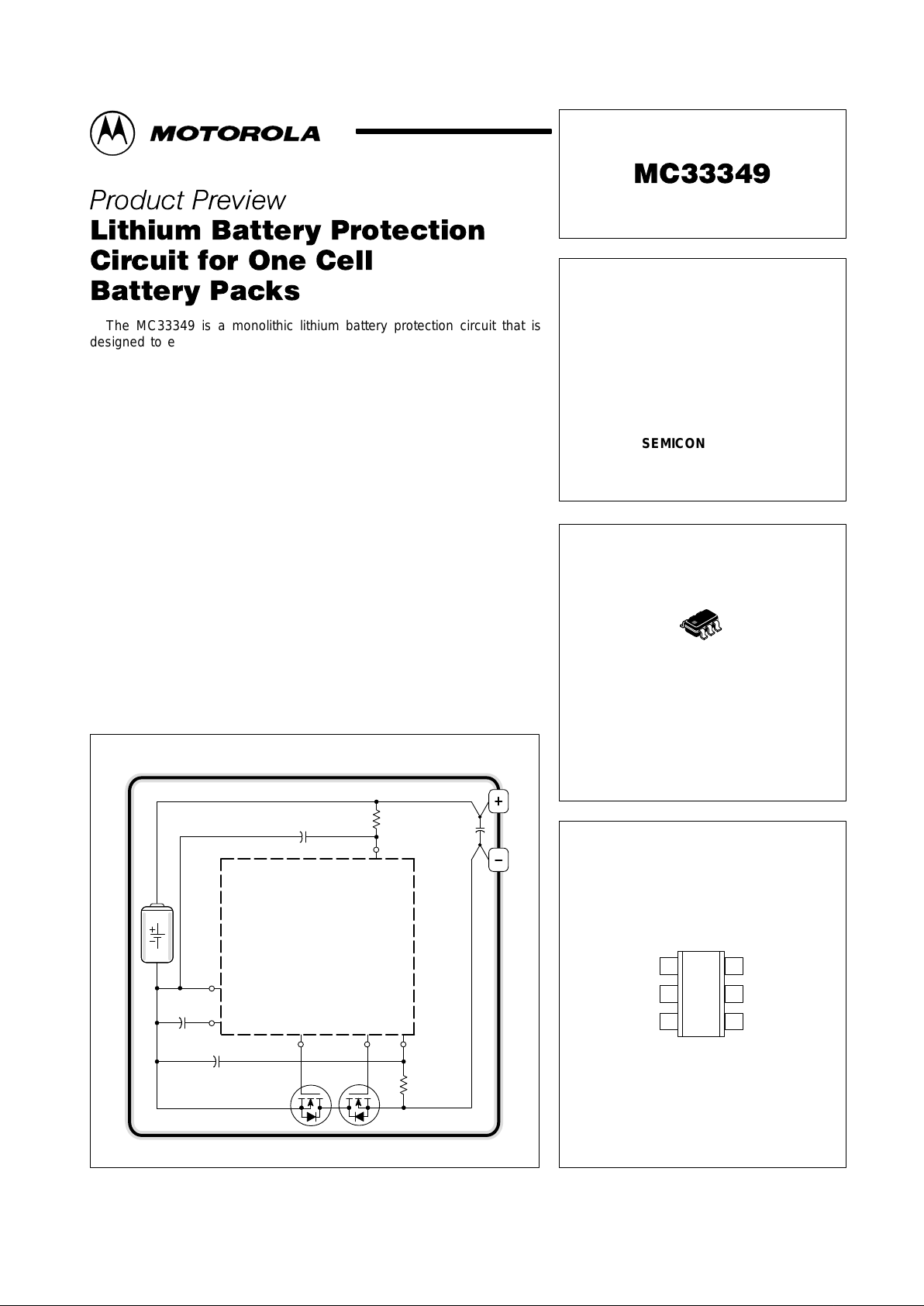
The MC33349 is a monolithic lithium battery protection circuit that is
designed to enhance the useful operating life of a one cell rechargeable
battery pack. Cell protection features consist of internally trimmed charge
and discharge voltage limits, charge and discharge current limit detection,
and a virtually zero current sleepmode state when the cell is discharged.
This protection circuit requires a minimum number of external components
and is targeted for inclusion within the battery pack. This MC33349 is
available in the SOT–23 6 lead surface mount package.
• Internally Trimmed Charge and Discharge Voltage Limits
• Charge and Discharge Current Limit Detection
• Virtually Zero Current Sleepmode State when Cells are Discharged
• Dedicated for One Cell Applications
• Minimum Components for Inclusion within the Battery Pack
• Available in a Low Profile Surface Mount Package
Ordering Information shown on following page.
Typical One Cell Smart Battery Pack
This device contains 264 active transistors.
132
5
6
4
MC33349
0.1 µF
0.1
µ
F
0.01
µ
F
100
Ω
1.0 k
Ω
This document contains information on a product under development. Motorola reserves the
right to change or discontinue this product without notice.
Motorola, Inc. 1998 Rev 0
MC33349
2
MOTOROLA ANALOG IC DEVICE DATA
ORDERING INFORMATION
Device
Charge
Overvoltage
Threshold (V)
Charge
Overvoltage
Hysteresis (mV)
Discharge
Undervoltage
Threshold (V)
Current Limit
Threshold (mV)
Operating
Temperature Range
Package
MC33349N–1 4.2
150
MC33349N–2 4.2
75
MC33349N–3 4.25
150
MC33349N–4 4.25
75
MC33349N–5 4.3
150
–
°
–
MC33349N–6 4.3
200
2.3
75
T
A
= –40 to
85°C
SOT–23
MC33349N–7 4.35 150
MC33349N–8 4.35 75
MC33349N–9 4.65 150
MC33349N–10
4.65 75
MAXIMUM RATINGS
Ratings Symbol Value Unit
Input Voltage
V
IR
V
Discharge Gate Drive Output (Pin 1) to Gnd (Pin 6) 5.0 to –1.0
Charge Gate Drive Common/Current Limit (Pin 2) to V
cell
(Pin 5)
1.0 to –18
Charge Gate Drive Output (Pin 3) to V
cell
(Pin 5) 1.0 to –18
Overvoltage Delay Capacitor (Pin 4) to Gnd (Pin 6) 5.0 to –1.0
Cell Voltage (Pin 5) to Gnd (Pin 6) 5.0 to –1.0
ББББББББББББББ
Thermal Resistance, Junction–to–Air
ÁÁ
R
θJA
ÁÁÁ
Á
°C/W
N Suffix, SOT–23 Plastic Package, Case 1262 TBD
Operating Junction Temperature (Note 1)
T
J
–40 to 85
°C
Storage Temperature
T
stg
–55 to 125
°C
MC33349
3
MOTOROLA ANALOG IC DEVICE DATA
ELECTRICAL CHARACTERISTICS (C
t
= 0.01 µF, TA = 25°C, for min/max values TA is the operating junction temperature range
that applies, unless otherwise noted.)
Characteristic
Symbol Min Typ Max Unit
VOLTAGE SENSING
Cell Charging Cutoff (Pin 5 to Pin 6)
ÁÁÁÁ
ÁÁÁ
Overvoltage Threshold, V
Cell
Increasing V
th(OV)
V
–1, –3 Suffix – 4.35 –
–2, –4 Suffix – 4.25 –
Overvoltage Hysteresis V
Cell
Decreasing V
H
– 200 – mV
Cell Discharging Cutoff (Pin 5 to Pin 6)
ÁÁÁÁ
ÁÁÁ
Undervoltage Threshold, V
Cell
Decreasing V
th(UV)
V
–1, –3 Suffix – 2.30 –
–2, –4 Suffix – 2.28 –
Input Bias Current During Cell Voltage Sample (Pin 5)
ÁÁÁÁ
I
IIB
–
20
–
ÁÁÁ
µA
Overvoltage Delay Time (V
cell
= 4.5 V) t
(ovd)
– 75 – ms
Unervoltage Delay Time (V
cell
= 2.1 V) t
(uvd)
– 13 – ms
Cell Voltage Sampling Period
ÁÁÁÁ
t
(smpl)
–
2.0
–
ÁÁÁ
ms
Cell Voltage Sampling Repitition Period t
(rep)
– 26 – ms
CURRENT SENSING
Discharge/Charge Current Limit (Pin 2 to Pin 6)
ÁÁÁÁ
ÁÁÁ
Discharge Threshold Voltage V
th(dschg)
mV
–1, –2 Suffix – 150 –
–3, –4 Suffix – 75 –
Discharge Current Hysteresis DCH – 50 – %
Charge Threshold Voltage V
th(chg)
mV
–1. –2 Suffix – –150 –
–3, –4 Suffix – –75 –
Charge Current Hysteresis CCH – 25 – %
Current Limit Delay Time (1.0 nF load @ CO & DO; to VDD/2)
Charge Gate Drive Output (Pin 3) t
(ccld)
– 10 – µs
Discharge Gate Drive Output (Pin 1) t
(dcld)
– 2.0 – µs
OUTPUTS
Charge Gate Drive Output Low (Pin 3 to Pin 2 @ IO = 50 µA)
ÁÁÁÁ
V
olc
–
0.2
–
ÁÁÁ
V
Charge Gate Drive Output High (Pin 5 to Pin 3 @ IO = –50 µA)
ÁÁÁÁ
V
ohc
–
0.1
–
ÁÁÁ
V
Discharge Gate Drive Output Low (Pin 1 to Pin 6 @ IO = 50 µA)
ÁÁÁÁ
V
old
–
0.2
–
ÁÁÁ
V
Discharge Gate Drive Output High (Pin 5 to Pin 1 @ IO = –50 µA)
ÁÁÁÁ
V
ohd
–
0.2
–
ÁÁÁ
V
TOTAL DEVICE
Average Cell Current
ÁÁÁÁ
I
cell
ÁÁÁ
Operating (V
cell
= 3.9 V) – 8.5 – µA
Sleepmode (V
cell
= 2.0 V) – 4.0 – nA
Minimum Operating Cell Voltage
ÁÁÁÁ
V
cell
–
1.5
–
ÁÁÁ
V

MC33349
4
MOTOROLA ANALOG IC DEVICE DATA
PIN FUNCTION DESCRIPTION
Pin Symbol Description
Á
Á
1
ÁÁÁ
Á
DO
ББББББББББББББББББББББББББ
Á
This output connects to the gate of discharge MOSFET switch Q2 allowing it to enable or disable battery pack
discharging.
Á
Á
Á
Á
2
ÁÁÁ
Á
ÁÁÁ
Á
P–
ББББББББББББББББББББББББББ
Á
ББББББББББББББББББББББББББ
Á
This is a multifunction pin that is used to monitor cell charge and discharge current and to provide a gate turn–off
path for charge switch Q1. A current limit fault is set when the combined voltage drop of charge switch Q1 and
discharge switch Q2 exceeds the discharge current limit threshold voltage, V
th(dschg)
above Pin 6 caused by a
load; or charge current limit threshold voltage, V
th(chg)
below Pin 6 caused by a charger.
Á
Á
3
ÁÁÁ
Á
CO
ББББББББББББББББББББББББББ
Á
This output connects to the gate of charge MOSFET switch Q1 allowing it to enable or disable battery pack
charging.
4
C
t
An external capacitor connects between this pin and ground (Pin 6) to set the sample timer frequency and
overvoltage delay time.
Á
Á
Á
Á
5
ÁÁÁ
Á
ÁÁÁ
Á
V
cell
ББББББББББББББББББББББББББ
Á
ББББББББББББББББББББББББББ
Á
This input connects to the positive terminal of the cell for voltage monitoring and provides operating bias for the
integrated circuit. Internally , the Cell Voltage Sample Switch periodically applies this voltage to a resistor divider
where it is compared by the Cell Voltage Detector to an internal reference.
6
Gnd
This is the ground pin of the IC.

MC33349
5
MOTOROLA ANALOG IC DEVICE DATA
PROTECTION CIRCUIT OPERATING MODE TABLE
Outputs
MOSFET Switches
БББББББББ
Á
Input Conditions
Cell Status
ББББББББББББББББ
Á
Circuit Operation
Battery Pack Status
Charge
Q1
ÁÁ
Á
Discharge
Q2
CELL CHARGING/DISCHARGING
БББББББББ
Storage or Nominal Operation:
No current or voltage faults
ББББББББББББББББ
Both Charge MOSFET Q1 and Discharge MOSFET Q2 are on. The
battery pack is available for charging or discharging.
ÁÁOnÁÁ
On
CELL CHARGING FAULT/RESET
БББББББББ
Á
БББББББББ
Á
БББББББББ
Á
Charge Voltage Limit Fault:
V
Pin 5
≥ V
th(OV)
for two consecutive
samples
ББББББББББББББББ
Á
ББББББББББББББББ
Á
ББББББББББББББББ
Á
Charge MOSFET Q1 is latched off and the cell is disconnected from
the charging source. An internal current source pull–up is applied to
divider resistors R1 and R2 creating a hysteresis voltage of VH. The
battery pack is available for discharging. Discharge current limit
protection is disabled.
ÁÁ
Á
ÁÁ
Á
ÁÁ
Á
On to Off
ÁÁ
Á
ÁÁ
Á
ÁÁ
Á
On
БББББББББ
Á
БББББББББ
Á
Charge Voltage Limit Reset:
V
Pin 5
< (V
th(OV)
– VH)
for one sample, or
V
Pin 2
> V
th(dschg)
ББББББББББББББББ
Á
ББББББББББББББББ
Á
Charge MOSFET Q1 will turn on when the voltage across the cell falls
sufficiently to overcome hysteresis voltage VH, or when a load is
applied to the battery pack.
ÁÁ
Á
ÁÁ
Á
Off to On
ÁÁ
Á
ÁÁ
Á
On
Charge Current Limit Fault:
V
Pin 2
≤ (V
Pin 6
+ V
th(chg)
)
Charge MOSFET Q1 is latched off and the cell is disconnected from
the charger. Q1 will remain in the of f state as long as V
Pin 6
exceeds
V
Pin 2
by ≈ V
th(chg)
. The battery pack is available for discharging.
Discharge current limit is disabled.
On to Off On
Charge Current Limit Reset:
V
Pin 6
– V
Pin 2
< V
th(chg)
The Sense Enable circuit will reset and turn on charge MOSFET Q1
when V
Pin 6
no longer exceeds V
Pin 2
by ≈ V
th(chg)
. This can be
accomplished by either disconnecting the charger from the battery
pack, or by connecting the battery pack to a load.
Off to On On
CELL DISCHARGING FAULT/RESET
БББББББББ
Á
БББББББББ
Á
Discharge Current Limit Fault:
V
Pin 2
≥ (V
Pin 6
+ V
th(dschg)
)
ББББББББББББББББ
Á
ББББББББББББББББ
Á
Discharge MOSFET Q2 is latched off and the cell is disconnected from
the load. Q2 will remain in the off state as long as V
Pin 2
exceeds V
Pin 6
by ≈ V
th(dschg)
. The battery pack is available for charging. Charge
current limit protection is disabled.
ÁÁ
Á
ÁÁ
Á
On
ÁÁ
Á
ÁÁ
Á
On to Off
БББББББББ
Á
БББББББББ
Á
Discharge Current Limit Reset:
V
Pin 2
– V
Pin 6
< V
th(dschg)
ББББББББББББББББ
Á
ББББББББББББББББ
Á
The Sense Enable circuit will reset and turn on discharge MOSFET Q2
when V
Pin 2
no longer exceeds V
Pin 5
by ≈ V
th(dschg)
. This can be
accomplished by either disconnecting the load from the battery pack, or
by connecting the battery pack to the charger.
ÁÁ
Á
ÁÁ
Á
On
ÁÁ
Á
ÁÁ
Á
Off to On
БББББББББ
Á
БББББББББ
Á
БББББББББ
Discharge Voltage Limit Fault:
V
Pin 5
≤ V
th(UV)
for one sample
ББББББББББББББББ
Á
ББББББББББББББББ
Á
ББББББББББББББББ
Discharge MOSFET Q2 is latched off, the cell is disconnected from the
load, and the protection circuit enters a low current sleepmode state.
The battery pack is available for charging. Charge current limit
protection is disabled.
ÁÁ
Á
ÁÁ
Á
ÁÁ
On
ÁÁ
Á
ÁÁ
Á
ÁÁ
On to Off
БББББББББ
Á
БББББББББ
Á
Discharge Voltage Limit Reset:
V
Pin 6
> (V
Pin 2
+ 0.6 V)
ББББББББББББББББ
Á
ББББББББББББББББ
Á
The Sense Enable circuit will reset and turn on discharge MOSFET Q2
when V
Pin 6
exceeds V
Pin 2
by 0.6 V . This can be accomplished by
connecting the battery pack to the charger.
ÁÁ
Á
ÁÁ
Á
On
ÁÁ
Á
ÁÁ
Á
Off to On
TEST MODE – PIN 4/PIN 5 SHORT
Continuous Charge Voltage Limit
Comparator
V
Pin 4
= V
Pin 5
= V
cell
< V
th(chg)
V
Pin 4
= V
Pin 5
= V
cell
> V
th(chg)
This condition occurs if Pin 4 and Pin 5 are accidently shorted together
or purposely connected for rapid Charge Voltgae Limit Testing.
MOSFET Q1 On to Off is not delayed and no hysteresis is required for
reset.
On
Off
On
On
FAULTY CELL
БББББББББ
Á
БББББББББ
Á
Discharge Voltage Limit Fault:
V
Pin 5
≤ 1.5 V
ББББББББББББББББ
Á
ББББББББББББББББ
Á
This condition can happen if the cell is defective (<1.5 V) or if a
momentary discharge current causes the cell voltage to fall below
V
th(UV)
before a sample is taken.
ÁÁ
Á
ÁÁ
Á
Off
ÁÁ
Á
ÁÁ
Á
Off

MC33349
6
MOTOROLA ANALOG IC DEVICE DATA
N SUFFIX
PLASTIC PACKAGE
CASE 1262–01
(SOT–23)
ISSUE O
OUTLINE DIMENSIONS
DIM MIN MAX
MILLIMETERS
A 0.90 1.45
A1 0.00 0.15
b 0.35 0.50
b1 0.35 0.45
c 0.09 0.20
c1 0.09 0.15
D 2.80 3.00
E 2.60 3.00
E1 1.50 1.75
e
0.95
e1
1.90
L 0.25 0.55
q
0 10
NOTES:
1. DIMENSIONS ARE IN MILLIMETERS.
2. INTERPRET DIMENSIONS AND TOLERANCES
PER ASME Y14.5M, 1994.
3. DIMENSION D DOES NOT INCLUDE FLASH OR
PROTRUSIONS. FLASH OR PROTRUSIONS
SHALL NOT EXCEED 0.23 PER SIDE.
4. TERMINAL NUMBERS ARE SHOWN FOR
REFERENCE ONLY.
5. DIMENSIONS D AND E1 ARE TO BE DETERMINED
AT DATUM PLANE H.
c
E
D
b
E1
1
2
3
6
5
4
PIN 1 INK MARK
IDENTIFIER
q
__
A
A
A
B
e1
e
M
0.20 CMB
0.05
C
M
0.10 C
S
A
A1
A
S
B
H
L
c1
b1
b
SECTION A–A

MC33349
7
MOTOROLA ANALOG IC DEVICE DATA
Motorola reserves the right to make changes without further notice to any products herein. Motorola makes no warranty , representation or guarantee regarding
the suitability of its products for any particular purpose, nor does Motorola assume any liability arising out of the application or use of any product or circuit, and
specifically disclaims any and all liability, including without limitation consequential or incidental damages. “T ypical” parameters which may be provided in Motorola
data sheets and/or specifications can and do vary in different applications and actual performance may vary over time. All operating parameters, including “Typicals”
must be validated for each customer application by customer’s technical experts. Motorola does not convey any license under its patent rights nor the rights of
others. Motorola products are not designed, intended, or authorized for use as components in systems intended for surgical implant into the body, or other
applications intended to support or sustain life, or for any other application in which the failure of the Motorola product could create a situation where personal injury
or death may occur. Should Buyer purchase or use Motorola products for any such unintended or unauthorized application, Buyer shall indemnify and hold Motorola
and its officers, employees, subsidiaries, affiliates, and distributors harmless against all claims, costs, damages, and expenses, and reasonable attorney fees
arising out of, directly or indirectly, any claim of personal injury or death associated with such unintended or unauthorized use, even if such claim alleges that
Motorola was negligent regarding the design or manufacture of the part. Motorola and are registered trademarks of Motorola, Inc. Motorola, Inc. is an Equal
Opportunity/Affirmative Action Employer.

MC33349
8
MOTOROLA ANALOG IC DEVICE DATA
Mfax is a trademark of Motorola, Inc.
How to reach us:
USA/EUROPE/Locations Not Listed: Motorola Literature Distribution; JAPAN: Nippon Motorola Ltd.: SPD, Strategic Planning Office, 141,
P.O. Box 5405, Denver, Colorado 80217. 1–303–675–2140 or 1–800–441–2447 4–32–1 Nishi–Gotanda, Shagawa–ku, Tokyo, Japan. 03–5487–8488
Customer Focus Center: 1–800–521–6274
Mfax: RMFAX0@email.sps.mot.com – TOUCHTONE 1–602–244–6609 ASIA/P ACIFIC: Motorola Semiconductors H.K. Ltd.; 8B Tai Ping Industrial Park,
Moto rola Fax Back System – US & Canada ONLY 1–800–774–1848 51 Ting Kok Road, Tai Po, N.T., Hong Kong. 852–26629298
– http://sps.motorola.com/mfax/
HOME PAGE: http://motorola.com/sps/
MC33349PP/D
◊
 Loading...