

Datasheet MC33348D-6, MC33348D-4, MC33348D-5, MC33348D-3, MC33348D-1 Datasheet (Motorola)
...
The MC33348 is a monolithic lithium battery protection circuit that is
designed to enhance the useful operating life of a one cell rechargeable
battery pack. Cell protection features consist of internally trimmed charge
and discharge voltage limits, discharge current limit detection with a
delayed shutdown, and a virtually zero current sleepmode state when the
cell is discharged. An additional feature includes an on–chip charge pump
for reduced MOSFET losses while charging or discharging a low cell
voltage battery pack. This protection circuit requires a minimum number of
external components and is targeted for inclusion within the battery pack.
This MC33348 is available in standard SOIC 8 lead surface mount
package.
• Internally Trimmed Charge and Discharge Voltage Limits
• Discharge Current Limit Detection with Delayed Shutdown
• Virtually Zero Current Sleepmode State when Cells are Discharged
• Charge Pump for Reduced Losses with a Low Cell Voltage Battery Pack
• Dedicated for One Cell Applications
• Minimum Components for Inclusion within the Battery Pack
• Available in a Low Profile Surface Mount Package
Order this document by MC33348/D
LITHIUM BATTERY
PROTECTION CIRCUIT
FOR
ONE CELL
SMART BATTERY PACKS
SEMICONDUCTOR
TECHNICAL DATA
8
1
Ordering Information shown on following page.
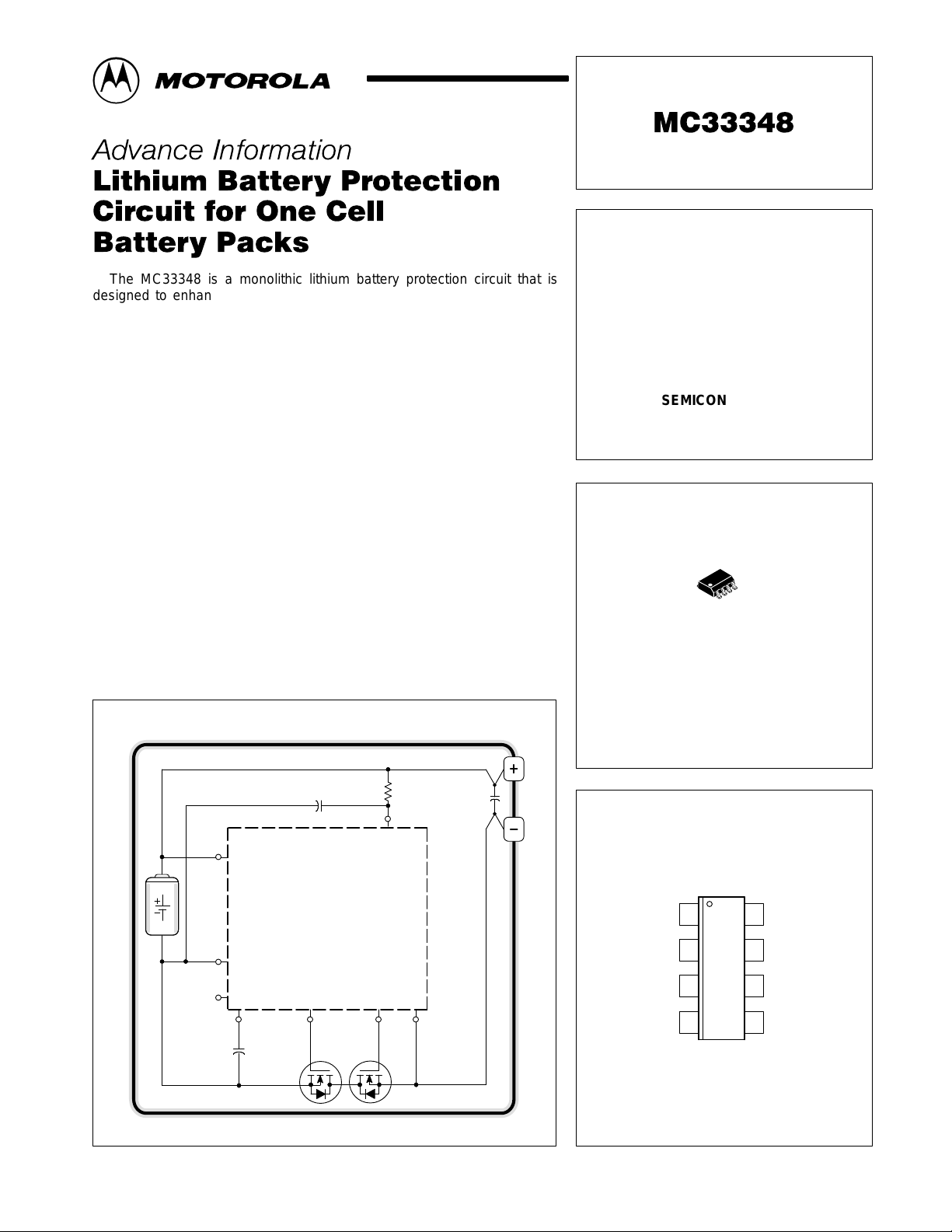
Typical One Cell Smart Battery Pack
Cell
Voltage
1
MC33348
Ground
3
T est
2
Charge Pump
8 Charge
Output
Discharge
Gate Drive
Output
4 6 5 Charge
Gate Drive
Output
7
V
CC
Gate Drive
Common/
Discharge
Current Limit
PLASTIC PACKAGE
PIN CONNECTIONS
Cell Voltage
Test
Ground
Discharge Gate
Drive Output
D SUFFIX
CASE 751
(SO–8)
18
2
3
4
(Top View)
Charge Pump
Output
V
7
CC
Charge Gate
6
Drive Output
Charge Gate Drive
5
Common/Discharge
Current Limit
This device contains 1170 active transistors.
This document contains information on a new product. Specifications and information herein
are subject to change without notice.
MOTOROLA ANALOG IC DEVICE DATA
Motorola, Inc. 1997 Rev 1
1
MC33348
4.20
2.25
4.25
300
2.28
T
25° to +85°C
SO–8
4.35
2.30
ORDERING INFORMATION
Charge
Overvoltage
Device
MC33348D–1
MC33348D–2
MC33348D–3
MC33348D–4
MC33348D–5
MC33348D–6
NOTE: Additional threshold limit options can be made available. Consult factory for information.
Threshold (V)
MAXIMUM RATINGS
Ratings Symbol Value Unit
Input Voltage (Measured with Respect to Ground, Pin 3)
Cell Voltage (Pin 1) 7.5
Test (Pin 2) 7.5
Discharge Gate Drive Output (Pin 4) 18
Charge Gate Drive Common/Discharge Current Limit (Pin 5) ±11
Charge Gate Drive Output (Pin 6) ±11
VCC (Pin 7) 7.5
Charge Pump Output (Pin 8) 10
Thermal Resistance, Junction–to–Air
D Suffix, SO–8 Plastic Package, Case 751 178
Operating Junction Temperature (Note 1)
Storage Temperature
NOTES: 1. Tested ambient temperature range for the MC33348:
T
= –25°CT
low
2.ESD data available upon request.
Charge
Overvoltage
Hysteresis (mV)
= +85°C
high
Discharge
Undervoltage
Threshold (V)
V
IR
R
θJA
T
J
T
stg
Discharge
Current Limit
Threshold (mV)
–40 to +150
–55 to +150
400
200
400
200
400
200
Operating
Temperature Range
–
= –
A
V
°C/W
°C
°C
Package
°
°
–
2
MOTOROLA ANALOG IC DEVICE DATA
MC33348
ÁÁÁÁ
ÁÁÁ
ÁÁÁÁ
ÁÁÁ
ÁÁÁÁ
ÁÁÁ
ÁÁÁÁ
ÁÁÁ
ÁÁÁÁ
ÁÁÁ
ÁÁÁÁ
ÁÁÁ
Á
ÁÁÁÁ
Á
Á
ÁÁÁ
Á
ÁÁÁÁ
ÁÁÁ
ELECTRICAL CHARACTERISTICS (V
= 4.0 V, TA = 25°C, for min/max values TA is the operating junction temperature range
CC
that applies (Note 1), unless otherwise noted.)
Characteristic
Symbol Min Typ Max Unit
VOLTAGE SENSING
Cell Charging Cutoff (Pin 1 to Pin 3)
Overvoltage Threshold, V
Increasing, TA = 25°C V
Cell
th(OV)
–1 Suffix 4.158 4.20 4.242
–2 Suffix 4.158 4.20 4.242
–3 Suffix 4.208 4.25 4.293
–4 Suffix 4.208 4.25 4.293
–5 Suffix 4.306 4.35 4.394
–6 Suffix 4.306 4.35 4.394
Overvoltage Hysteresis V
Decreasing V
Cell
H
–1 Suffix – 300 –
–2 Suffix – 300 –
–3 Suffix – 300 –
–4 Suffix – 300 –
–5 Suffix – 300 –
–6 Suffix – 300 –
Cell Discharging Cutoff (Pin 1 to Pin 3, TA = 25°C)
Undervoltage Threshold, V
Decreasing V
Cell
th(UV)
–1 Suffix 2.205 2.25 2.295
–2 Suffix 2.205 2.25 2.295
–3 Suffix 2.234 2.28 2.326
–4 Suffix 2.234 2.28 2.326
–5 Suffix 2.254 2.30 2.346
–6 Suffix 2.254 2.30 2.346
Input Bias Current During Cell Voltage Sample (Pin 1)
Cell Voltage Sampling Rate
I
IB
t
(smpl)
–
–
28
1.0
–
–
CURRENT SENSING
Discharge Current Limit (Pin 3 to Pin 5, TA = 25°C)
Threshold Voltage V
th(dschg)
–1 Suffix 360 400 440
–2 Suffix 180 200 220
–3 Suffix 360 400 440
–4 Suffix 180 200 220
–5 Suffix 360 400 440
–6 Suffix 180 200 220
Delay I
dly(dschg)
1.0 2.3 4.0 ms
CHARGE PUMP
Output Voltage (Pin 8, RL ≥ 1010, TA = 25°C)
V
O
8.0
10.2
12
TOTAL DEVICE
Average Cell Current (TA = 25°C, Battery Pack Unloaded and without
БББББББББББББББББ
Current Limit Fault)
I
CC
ÁÁÁ
ÁÁÁÁÁÁÁÁÁ
Operating (VCC = 4.0 V) – 17 20 µA
Sleepmode (VCC = 2.0 V) – 2.0 – nA
Minimum Operating Cell Voltage for Logic and Gate Drivers
NOTE: 1.Tested ambient temperature range for the MC33348:
T
= –25°CT
low
high
= +85°C
V
CC
–
1.5
–
V
mV
V
µA
s
mV
V
ÁÁ
V
MOTOROLA ANALOG IC DEVICE DATA
3
MC33348
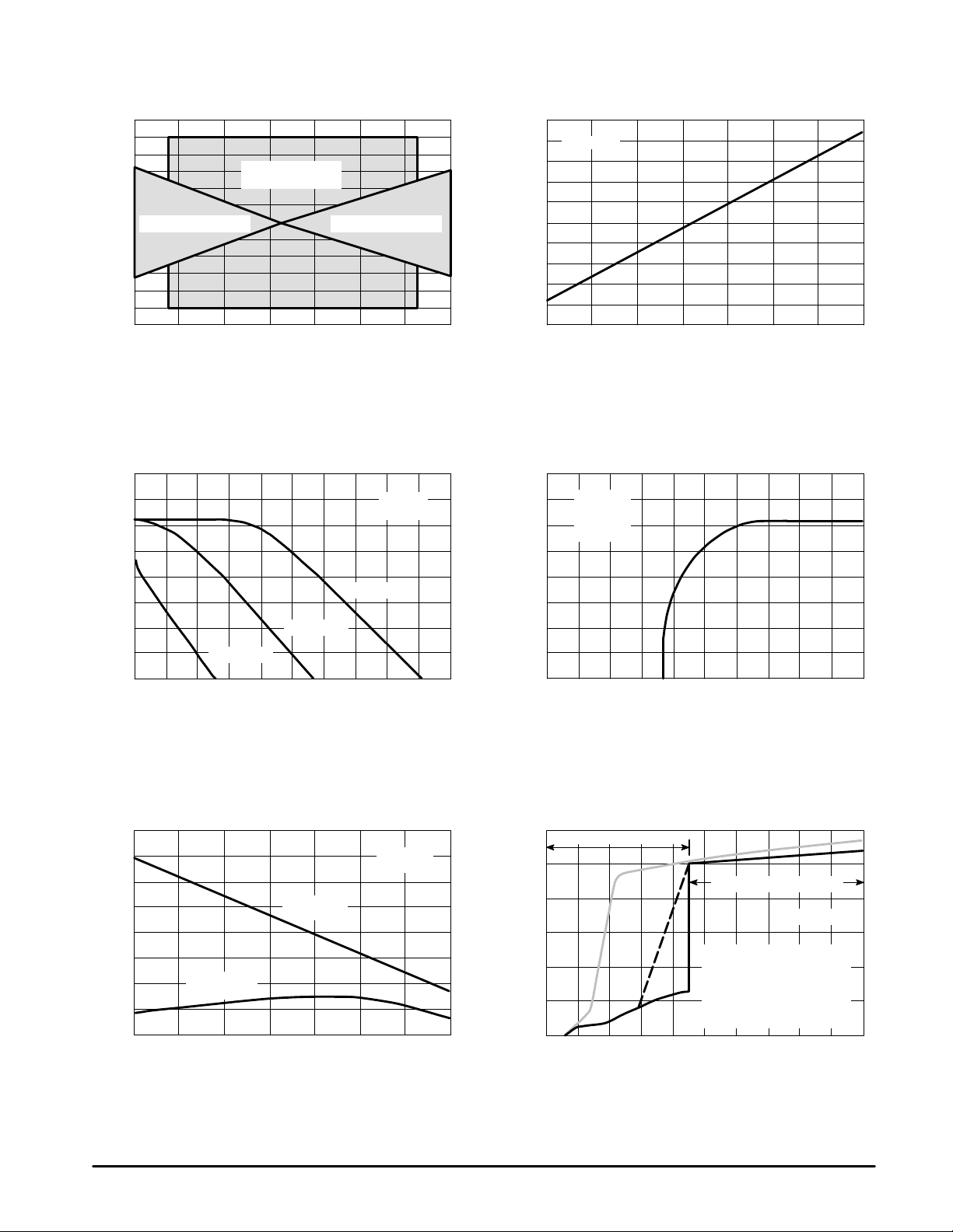
Figure 1. Charge and Discharge
Threshold V oltage Change versus Temperature
1.2
0.8
Maximum Threshold
0.4
0
Typical Threshold Change Typical Threshold Change
Charge Limits
–0.4
, THRESHOLD VOLTAGE CHANGE (%)
–0.8
–1.2
th(OV & UV)
V
∆
TA, AMBIENT TEMPERATURE (°C) TA, AMBIENT TEMPERATURE (°C)
Figure 3. Gate Drive Output Voltage
12
10
versus Load Current
CO = 10 nF
°
C
TA = 25
Figure 2. Discharge Current Limit
Threshold V oltage Change versus Temperature
16
VCC = 4.0 V
8.0
0
, CURRENT LIMIT THRESHOLD
–8.0
VOLTAGE CHANGE (%)
th(dschg)
–16
V
∆
1004020–20–40 0 60 80 1004020–20–40 0 60 80
Figure 4. Gate Drive Output Voltage
12
10
CO = 10 nF
Pin 2 = Gnd
RL ≥ 1010
TA = 25°C
versus Supply V oltage
Ω
8.0
6.0
, GATE DRIVE OUTPUT VOLTAGE (V)
O
V
4.0
12
11
10
9.0
, CHARGE PUMP OUTPUT VOL TAGE (V)
O
V
8.0
VCC = 4.15 V
VCC = 3.25 V
VCC = 2.35 V
IL, OUTPUT LOAD CURRENT (µA) VCC, SUPPLY VOLTAGE (V)
Figure 5. Charge Pump Output Voltage
versus T emperature
CO = 10 nF
≥
1010
RL
VCC = 4.15 V
In Regulation
VCC = 2.35 V
Out of Regulation
8.0
6.0
, GATE DRIVE OUTPUT VOLTAGE (V)
O
V
1.00.80.60.20 0.4
4.0
4.0
5.01.00 2.0 3.0
Figure 6. Supply Current
2
10
Battery Pack Sleepmode Range
1
Ω
1004020–20–40 0 60 80
10
µ
0
10
–1
10
–2
10
, SUPPLY CURRENT ( A)
CC
I
–3
10
–4
10
0 1.0 2.0 3.0 5.0
versus Supply V oltage
Battery Pack Operating Range
123
1 – Battery pack unloaded without
discharge current limit fault.
2 – Battery pack loaded without
discharge current limit fault.
3 – Battery pack loaded or unloaded
with discharge current limit fault.
VCC, SUPPLY VOLTAGE (V)TA, AMBIENT TEMPERATURE (°C)
TA = 25°C
4.0
4
MOTOROLA ANALOG IC DEVICE DATA

MC33348
Á
Á
Á
Á
Á
Á
Á
Á
Á
Á
Á
Á
Á
Á
Á
Á
Á
Á
Á
Á
Á
Á
Á
Á
Á
Á
Á
Á
Á
Á
Á
Á
Á
Á
Á
Á
Á
Á
Á
Á
Á
Á
Á
Á
Á
Á
Á
Á
Á
Á
Á
Á
Á
Á
Á
Á
Á
Á
Á
Á
Á
Á
Á
Á
Á
Á
Á
Á
Á
Á
Á
Á
Á
Á
Á
Á
Á
Á
PROTECTION CIRCUIT OPERATING MODE TABLE
Outputs
MOSFET Switches
Input Conditions
БББББББ
Cell Status
БББББББББББББББ
Circuit Operation
Battery Pack Status
Charge
Q1
DischargeQ2Charge
ÁÁ
CELL CHARGING/DISCHARGING
Storage or Nominal Operation:
No current or voltage faults
БББББББ
Both Charge MOSFET Q1 and Discharge MOSFET Q2 are on.
The battery pack is available for charging or discharging.
БББББББББББББББ
ÁÁOnÁÁOnÁÁ
CELL CHARGING FAULT/RESET
Charge Voltage Limit Fault:
БББББББ
V
≥ V
Pin 1
БББББББ
БББББББ
th(OV)
for 1.0 s
Charge Voltage Limit Reset:
V
< (V
Pin 1
БББББББ
for 1.0 s
БББББББ
th(OV)
– VH)
Charge MOSFET Q1 is latched off and the cell is disconnected
БББББББББББББББ
from the charging source. An internal current source pull–up is
applied to divider resistors R1 and R2 creating a hysteresis
БББББББББББББББ
voltage of VH. The battery pack is available for discharging.
БББББББББББББББ
Discharge current limit protection is disabled.
Charge MOSFET Q1 will turn on when the voltage across the cell
falls sufficiently to overcome hysteresis voltage VH. This can be
БББББББББББББББ
accomplished by applying a load to the battery pack. Discharge
БББББББББББББББ
current limit protection is enabled.
On to Off
ÁÁ
ÁÁ
ÁÁ
Off to On
ÁÁ
ÁÁ
On
ÁÁ
ÁÁ
ÁÁ
On
ÁÁ
ÁÁ
CELL DISCHARGING FAULT/RESET
Discharge Current Limit Fault:
V
≥ (V
Pin 5
БББББББ
for 3.0 ms and
V
БББББББ
БББББББ
БББББББ
БББББББ
< (V
Pin 1
for 1.0 ms
Discharge Current Limit Reset:
V
– V
Pin 5
Pin 3
th(OV)
Pin 3
+ V
– VH)
< V
th(dschg)
th(dschg)
Discharge Voltage Limit Fault:
V
≤ V
Pin 1
БББББББ
consecutive 1.0 s samples
th(UV)
for three
Discharge Voltage Limit Reset:
БББББББ
V
> (V
Pin 3
БББББББ
FAULTY CELL
ББББББББББББББББББББББББББББББББ
Discharge Voltage Limit Fault:
БББББББ
V
≤ 1.5 V
Pin 1
БББББББ
Pin 5
+ 0.6 V)
Discharge MOSFET Q2 is latched off and the cell is
)
disconnected from the load. Q2 will remain in the off state as long
БББББББББББББББ
as V
available for charging.
БББББББББББББББ
The Sense Enable circuit will reset and turn on discharge
БББББББББББББББ
MOSFET Q2 when V
≈ V
БББББББББББББББ
the load from the battery pack, or by connecting the battery pack
БББББББББББББББ
to the charger.
exceeds V
Pin 5
th(dschg)
by ≈ V
Pin 3
Pin 3
. This can be accomplished by either disconnecting
th(dschg)
no longer exceeds V
. The battery pack is
by
Pin 5
Discharge MOSFET Q2 is latched off, the cells are disconnected
from the load, and the protection circuit enters a low current
БББББББББББББББ
sleepmode state. The battery pack is available for charging.
The Sense Enable circuit will reset and turn on discharge
БББББББББББББББ
MOSFET Q2 when V
accomplished by connecting the battery pack to the charger.
БББББББББББББББ
This condition can happen if the cell is defective (<1.5 V). The
БББББББББББББББ
protection circuit logic will not function and the battery pack
cannot be charged.
БББББББББББББББ
Pin 3
exceeds V
by 0.6 V. This can be
Pin 5
On
ÁÁ
ÁÁ
On
ÁÁ
ÁÁ
ÁÁ
On
ÁÁ
On
ÁÁ
ÁÁ
Disabled
ÁÁ
ÁÁ
On to Off
ÁÁ
ÁÁ
Off to On
ÁÁ
ÁÁ
ÁÁ
On to Off
ÁÁ
Off to On
ÁÁ
ÁÁ
Disabled
ÁÁ
ÁÁ
Function
Pump
Active
Active
ÁÁ
ÁÁ
ÁÁ
Active
ÁÁ
ÁÁ
Active
ÁÁ
ÁÁ
Active
ÁÁ
ÁÁ
ÁÁ
Disabled
ÁÁ
Active
ÁÁ
ÁÁ
Disabled
ÁÁ
ÁÁ
MOTOROLA ANALOG IC DEVICE DATA
5

MC33348
Á
Á
Á
Á
Á
Á
Á
Á
Á
Á
Á
Á
Á
Á
Á
Á
Á
Á
Á
Á
Á
Figure 7. One Cell Smart Battery Pack
Cell
Cell
Voltage
1
Ground
3
Test
2
Charge Pump
MC33348
Cell Voltage
Sample
Switch
2.0 k
Ck
Oscillator
Ck
En
Charge Pump
8 Charge
C
O
Discharge
Gate Drive
Output
Discharge
Switch Q2
Output
0.01
10
Over/Under
Cell Voltage
Detector
&
Reference
Discharge
Over/Under
Data Latch
Overcurrent
Detector
&
Control Logic
Sense
Enable
Charge/Discharge
Gate Drivers
4 6 5 Charge
Gate Drive
Output
Charge
Switch
Q1
Gate Drive
Common/
Discharge
Current Limit
5.1 k
R1
R2
R3
7VCC
C
0.1
I
1.0 M
Components CI is mandatory. Refer to the Battery Pack Application text.
PIN FUNCTION DESCRIPTION
Pin Symbol Description
1
Cell Voltage
Á
Á
Á
Á
БББББ
БББББ
2
Test
БББББ
3
Ground
4
Discharge Gate Drive
Output
БББББ
5
Charge Gate Drive
Common/Discharge
Á
Á
Á
БББББ
Current Limit
БББББ
6
Charge Gate Drive
БББББ
Output
7
V
CC
8
Charge Pump Output
This input is connected to the positive terminal of the cell for voltage monitoring. Internally, the Cell
ББББББББББББББББББББББББ
Voltage Sample Switch applies this voltage to a resistor divider where it is compared by the Cell Voltage
Detector to an internal reference.
ББББББББББББББББББББББББ
This pin is normally not connected and is used in testing the protection IC. An active low at this input
resets the internal logic and turns on both MOSFET switches. Upon release, the logic becomes active and
ББББББББББББББББББББББББ
the cell voltage is sampled within 1.0 ms.
This is the protection IC ground and all voltage ratings are with respect to this pin.
This output connects to the gate of discharge switch Q2 allowing it to enable or disable battery pack
discharging.
ББББББББББББББББББББББББ
This is a multifunction pin that is used to monitor cell discharge current and to provide a gate turn–off
path for charge switch Q1. A discharge current limit fault is set when the battery pack load causes the
ББББББББББББББББББББББББ
combined voltage drop of charge switch Q1 and discharge switch Q2 to exceed the discharge current limit
threshold voltage, V
ББББББББББББББББББББББББ
This output connects to the gate of charge switch Q1 allowing it to enable or disable battery pack
ББББББББББББББББББББББББ
charging.
th(dschg)
, with respect to Pin 3.
This pin is the positive supply voltage for the protection IC.
This is the charge pump output. A reservoir capacitor is connected from this pin to ground.
6
MOTOROLA ANALOG IC DEVICE DATA

MC33348
ББББББ
ББББББ
INTRODUCTION
The insatiable demand for smaller lightweight portable
electronic equipment has dramatically increased the
requirements of battery performance. Batteries are expected
to have higher energy densities, superior cycle life, be safe in
operation and environmentally friendly. To address these
high expectations, battery manufacturers have invested
heavily in developing rechargeable lithium–based cells.
Today’s most attractive chemistries include lithium–polymer,
lithium–ion, and lithium–metal. Each of these chemistries
require electronic protection in order to constrain cell
operation to within the manufacturers limits.
Rechargeable lithium–based cells require precise charge
and discharge termination limits for both voltage and current
in order to maximize cell capacity, cycle life, and to protect
the end user from a catastrophic event. The termination limits
are not as well defined as with older non–lithium chemistries.
These limits are dependent upon a manufacturer’s particular
lithium chemistry, construction technique, and intended
application. Battery pack assemblers may also choose to
enhance cell capacity at the expense of cycle life. In order to
address these requirements, six versions of the MC33348
protection circuit were developed. These devices feature
charge overvoltage protection, discharge current limit
protection with delayed shutdown, low operating current, a
virtually zero current sleepmode state, and requires few
external components to implement a complete one cell smart
battery pack.
Operating Description
The MC33348 is specifically designed to be placed in the
battery pack where it is continuously powered from a single
lithium cell. In order to maintain cell operation within specified
limits, the protection circuit senses both cell voltage and
discharge current, and correspondingly controls the state of
two N–channel MOSFET switches. These switches, Q1 and
Q2, are placed in series with the negative terminal of the Cell
and the negative terminal of the battery pack. This
configuration allows the protection circuit to interrupt the
appropriate charge or discharge path FET in the event that
either a voltage threshold or the discharge current limit for the
cell has been exceeded.
Figure 8. One Cell Smart Battery Pack
A functional description of the protection circuit blocks
follows. Refer to the detailed block diagram shown in
Figure 7.
Voltage Sensing
Voltage sensing is accomplished by the use of the Cell
Voltage Sample Switch in conjunction with the Over/Under
Voltage Detector and Reference block. The Sample Switch
applies the cell voltage to the top resistor of an internal
divider string. The voltage at each of the tap points is
sequentially polled and compared to an internal reference. If
a limit has been exceeded, the result is stored in the
Over/Under Data Latch and Control Logic block. The Cell
Voltage Sample Switch is gated on for a 1.0 ms period at a
one second repetition rate. This low duty cycle sampling
technique reduces the average load current that the divider
presents across the cell, thus extending the useful battery
pack capacity. The cell voltage limits are tested in the
following sequence:
Figure 9. Cell Sensing Sequence
Polling
Sequence
БББББ1ÁÁÁÁ
БББББ2ÁÁÁÁ
Time
(ms)
0.5
0.5
Tested
Limit
Overvoltage
БББББ
Undervoltage
БББББ
By incorporating this polling technique with a single
comparator and voltage divider, a significant reduction of
circuitry and trim elements is achieved. This results in a
smaller die size, lower cost, and reduced operating current.
Figure 10. Cell V oltage Limit Sampling
From
Cell Voltage
Sample Switch
Over/Under
Cell Voltage
Detector
&
Reference
To
Cell Negative
Terminal
Cell Voltage
Discharge Voltage
Threshold
Charge Voltage
Threshold
Cell Voltage
Return
R1
R2
R3
+
Cell
Voltage
–
MOTOROLA ANALOG IC DEVICE DATA
Cell
1
3
84 65
Discharge
MOSFET Q2
MC33348
7
Charge
MOSFET Q1
The cell charge and discharge voltage limits are controlled
by the values selected for the internal resistor divider string
and the comparator input threshold. As the battery pack
reaches full charge, the Cell Voltage Detector will sense an
overvoltage fault condition when the cell exceeds the
designed overvoltage limit. The fault information is stored in
a data latch and charge MOSFET Q1 is turned off,
disconnecting the battery pack from the charging source. An
internal current source pull–up is then applied to lower tap of
the divider, creating a hysteresis voltage. As a result of an
overvoltage fault, the battery pack is available for
discharging only .
The overvoltage fault is reset by applying a load to the
battery pack. As the voltage across the cell falls below the
hysteresis level, charge MOSFET Q1 will turn on and the
current source pull–up will turn off. The battery pack will now
be available for charging or discharging.
7

MC33348
Á
Á
Á
Á
As the load eventually depletes the battery pack charge,
the Cell Voltage Detector will sense an undervoltage fault
condition when the cell falls below the designed undervoltage
limit. After three consecutive faults are detected, discharge
MOSFET Q2 is turned off, disconnecting the battery pack
from the load. The protection circuit will now enter a low
current sleepmode state. Refer to Figure 6. As a result of the
undervoltage fault, the battery pack is available for charging
only . The typical cutof f thresholds and hysteresis voltage are
shown in Figure 1 1.
Figure 11. Cutoff and Hysteresis Limits
Device
ÁÁ
Suffix
–1, –2
–3, –4
–5, –6
Charging
Cutoff
ÁÁÁ
(V)
4.20
4.25
4.35
Hysteresis
ÁÁÁÁ
(mV)
300
300
300
The undervoltage logic is designed to automatically reset
if less than three consecutive faults appear. This helps to
prevent a premature disconnection of the load during high
current pulses when the battery pack charge is close to
being depleted.
The undervoltage fault is reset by applying charge current
to the battery pack. When the voltage on Pin 3 exceeds Pin 5
by 0.6 V, discharge MOSFET Q2 will turn on. The battery
pack will now be available for charging or discharging.
Figure 12. Additional Discharge Current Limit Delay
Disharging
Cutoff
ÁÁÁ
(V)
2.25
2.28
2.30
Current Sensing
Discharge current limit protection is internally provided by
the MC33348. As the battery pack discharges, Pins 5 and 3
sense the voltage drop across MOSFETs Q1 and Q2. A
discharge current limit fault is detected if the voltage at Pin 5
is greater than Pin 3 by 400 mV for –1, –3 and –5 suffix
devices, or 200 mV for –2, –4 and –6 suffix devices. The fault
information is stored in a data latch and discharge MOSFET
Q2 is turned off, disconnecting the battery pack from the load.
As a result of the discharge current fault, the battery pack is
available for charging only. The discharge current limit is
given by:
I
Lim(dschg)
+
V
R
th(dschg)
Lim(dschg)
+
R
V
th(dschg)
DS(on)Q1
)
R
DS(on)Q2
The discharge current fault is reset by either disconnecting
the load from the battery pack, or by connecting the battery
pack to the charger. When the voltage on Pin 5 no longer
exceeds Pin 3 by approximately V
th(dschg)
, the Sense Enable
circuit will turn on discharge MOSFET Q2.
Figure 13. Power Supply Decoupling
C
10
1
Cell
R
5.1 k
7
MC33348
3
84 65
C
dly
R
dly
The discharge current limit shutdown delay time is typically
3.0 ms. This time can be extended with the addition of
components R
dly
and C
. With an R
dly
of 5.1 k and C
dly
dly
of 10
µF, the current limit shutdown time is extended to 40 ms.
The additional discharge current limit delay circuitry must
not be used if the anticipated open–circuit charger voltage
will exceed 6.0 V. When the charger causes the battery pack
input to exceed 6.0 V , additional current will flow out of Pin 5,
creating a voltage drop across resistor R
. This voltage drop
dly
causes the source of MOSFET Q1 to fall below it’s gate,
allowing it to unexpectedly turn back on.
MC33348
3
In order to guarantee proper discharge current limit
operation when the battery pack output is shorted, power
must be made available to the MC33348. This can be
accomplished by decoupling the VCC input with the R/C
component values shown above. The capacitor value must
be increased to 100 µF if the discharge current limit
shutdown delay time is extended to 40 ms as shown in
Figure 12. A small signal schottky diode can be used in place
of R for enhanced short circuit operation. The diode cathode
is connected to Pin 7 and C, and the anode is connected to
the positive terminal of the cell. The schottky diode solution
may be a better choice in applications that have a charger
with a relatively high open circuit voltage. These components
can be deleted if operation of the discharge current limit is not
required when the battery pack output is shorted.
8
MOTOROLA ANALOG IC DEVICE DATA

MC33348
As previously stated in the voltage sensing operating
description, charge MOSFET Q1 is held off during an
overvoltage fault condition. When this condition is present,
the discharge current limit protection function is internally
disabled. This is required, since the voltage across Q1, in the
off state, would exceed the current sense threshold. This
would cause Q2 to turn off as well, preventing both charging
and discharging of the cell. Discharge current limit protection
is enabled whenever an overvoltage fault is not present.
The discharge current protection circuit contains a built in
response delay of 3.0 ms. This helps to prevent fault
activation when the battery pack is subjected to pulsed
currents during discharging. An additional current sense
delay can be added as shown in Figure 12. If the battery pack
is subjected to extremely high discharge current pulses or is
shorted, the VCC pin must be decoupled from the cell. This is
required so that the protection circuit will have sufficient
operating voltage during the load transient, to ensure turn off
of discharge MOSFET Q2. Figure 13 shows the placement of
decoupling components.
Charge Pump and MOSFET Switches
The MC33348 contains an on chip Charge Pump to
ensure that the MOSFET switches are fully enhanced for
reduced power losses. An external reservoir capacitor
normally connects from the Charge Pump output to ground,
Pins 8 and 3. The capacitor value is not critical and is usually
within the range of 10 nF to 100 nF. The Charge Pump output
is regulated at 10.2 V allowing the use of the more
economical logic level MOSFETs. The main requirement in
selecting a particular type of MOSFET switch is to consider
the desired on–resistance at the lowest anticipated operating
voltage of the battery pack. A table of small outline surface
mount devices is given in Figure 14. When using extremely
low threshold MOSFETs, it may be desirable to disable the
Charge Pump so that the maximum gate to source voltage is
not exceeded. This can be accomplished by connecting Pin 6
to Pin 5, and will result in an additional cell drain current of
approximately 8.0 µA.
T esting
A test pin is provided in order to speed up device and
battery pack testing. By grounding Pin 2, the internal logic is
held in a reset state and both MOSFET switches are turned
on. Upon release, the logic becomes active and the cell
voltage is polled within 1.0 ms.
Battery Pack Application
The one cell smart battery pack application shown in
Figure 7 contains a capacitor labeled CI that connects
directly across the battery pack terminals. This component
prevents excessive currents from flowing into the MC33348
when the battery pack terminals are shorted or arced, and is
mandatory. Capacitor CI is a 100 nF ±20% ceramic leaded
or surface mount type. It must be placed directly across the
battery pack plus and minus terminals with extremely short
lead lengths (≤1/16″).
In applications where inordinately low leakage MOSFETs
are used, the protection circuit may take a considerable
amount of time to reset from an overcurrent fault after the
load is removed. This situation can be remedied by providing
a small leakage path for charging CI, thus allowing Pin 5 to
rapidly fall below the discharge current limit threshold. A
1.0 megohm resistor placed across the MOSFET switches
accomplishes this task with a minimum increase in cell
discharge current when the battery pack is connected to a
load.
ББББББББББББББББББББББББББББББББ
Device
ÁÁÁÁ
Type
ÁÁÁÁ
MMFT3055VL
ÁÁÁÁ
MMDF3N03HD
ÁÁÁÁ
MMDF4N01HD
ÁÁÁÁ
MMSF5N02HD
ÁÁÁÁ
MMDF6N02HD
БББББББББББББББББББББББББББ
2.5 V
ÁÁÁ
ÁÁÁ–ÁÁÁ–ÁÁÁ–ÁÁÁ
ÁÁÁ–ÁÁÁ
0.047 Ω
ÁÁÁ
ÁÁÁ–ÁÁÁ
0.043 Ω
Figure 14. Small Outline Surface Mount MOSFET Switches
On–Resistance (Ω) versus Gate to Source Voltage (V)
3.0 V
ÁÁÁ
0.525 Ω
0.042 Ω
ÁÁÁ
0.065 Ω
0.035 Ω
4.0 V
ÁÁÁ
0.080 Ω
ÁÁÁ
0.037 Ω
ÁÁÁ
0.023 Ω
ÁÁÁ
0.029 Ω
5.0 V
ÁÁÁ
0.120 Ω
0.065 Ω
ÁÁÁ
0.035 Ω
ÁÁÁ
0.021 Ω
ÁÁÁ
0.028 Ω
6.0 V
ÁÁÁ
0.115 Ω
ÁÁÁ
0.063 Ω
ÁÁÁ
0.034 Ω
ÁÁÁ
0.020 Ω
ÁÁÁ
0.026 Ω
7.5 V
ÁÁÁ
0.108 Ω
ÁÁÁ
0.062 Ω
ÁÁÁ
0.033 Ω
ÁÁÁ
0.018 Ω
ÁÁÁ
0.025 Ω
9.0 V
ÁÁÁ
0.100 Ω
ÁÁÁ
0.060 Ω
ÁÁÁ
0.033 Ω
ÁÁÁ
0.018 Ω
ÁÁÁ
0.023 Ω
MOTOROLA ANALOG IC DEVICE DATA
9

MC33348
OUTLINE DIMENSIONS
D SUFFIX
PLASTIC PACKAGE
CASE 751–05
(SO–8)
ISSUE S
C
A
E
B
A1
D
58
0.25MB
1
H
4
e
M
h
X 45
_
q
C
A
SEATING
PLANE
0.10
L
B
SS
A0.25MCB
NOTES:
1. DIMENSIONING AND TOLERANCING PER ASME
Y14.5M, 1994.
2. DIMENSIONS ARE IN MILLIMETERS.
3. DIMENSION D AND E DO NOT INCLUDE MOLD
PROTRUSION.
4. MAXIMUM MOLD PROTRUSION 0.15 PER SIDE.
5. DIMENSION B DOES NOT INCLUDE MOLD
PROTRUSION. ALLOWABLE DAMBAR
PROTRUSION SHALL BE 0.127 TOTAL IN EXCESS
OF THE B DIMENSION AT MAXIMUM MATERIAL
CONDITION.
MILLIMETERS
DIM MIN MAX
A 1.35 1.75
A1 0.10 0.25
B 0.35 0.49
C 0.18 0.25
D 4.80 5.00
E
3.80 4.00
1.27 BSCe
H 5.80 6.20
h
0.25 0.50
L 0.40 1.25
0 7
q
__
10
MOTOROLA ANALOG IC DEVICE DATA

MC33348
Motorola reserves the right to make changes without further notice to any products herein. Motorola makes no warranty , representation or guarantee regarding
the suitability of its products for any particular purpose, nor does Motorola assume any liability arising out of the application or use of any product or circuit, and
specifically disclaims any and all liability, including without limitation consequential or incidental damages. “T ypical” parameters which may be provided in Motorola
data sheets and/or specifications can and do vary in different applications and actual performance may vary over time. All operating parameters, including “Typicals”
must be validated for each customer application by customer’s technical experts. Motorola does not convey any license under its patent rights nor the rights of
others. Motorola products are not designed, intended, or authorized for use as components in systems intended for surgical implant into the body, or other
applications intended to support or sustain life, or for any other application in which the failure of the Motorola product could create a situation where personal injury
or death may occur. Should Buyer purchase or use Motorola products for any such unintended or unauthorized application, Buyer shall indemnify and hold Motorola
and its officers, employees, subsidiaries, affiliates, and distributors harmless against all claims, costs, damages, and expenses, and reasonable attorney fees
arising out of, directly or indirectly, any claim of personal injury or death associated with such unintended or unauthorized use, even if such claim alleges that
Motorola was negligent regarding the design or manufacture of the part. Motorola and are registered trademarks of Motorola, Inc. Motorola, Inc. is an Equal
Opportunity/Affirmative Action Employer.
MOTOROLA ANALOG IC DEVICE DATA
11

MC33348
How to reach us:
USA/EUROPE/Locations Not Listed: Motorola Literature Distribution; JAPAN: Nippon Motorola Ltd.: SPD, Strategic Planning Office, 4–32–1,
P.O. Box 5405, Denver, Colorado 80217. 1–303–675–2140 or 1–800–441–2447 Nishi–Gotanda, Shinagawa–ku, Tokyo 141, Japan. 81–3–5487–8488
Customer Focus Center: 1–800–521–6274
Mfax: RMFAX0@email.sps.mot.com – TOUCHTONE 1–602–244–6609 ASIA/PACIFIC: Motorola Semiconductors H.K. Ltd.; 8B Tai Ping Industrial Park,
Moto rola Fax Back Syst em – US & Canada ONLY 1–800–774–1848 51 Ting Kok Road, Tai Po, N.T ., Hong Kong. 852–26629298
HOME PAGE: http://motorola.com/sps/
12
– http://sps.motorola.com/mfax/
◊
MOTOROLA ANALOG IC DEVICE DATA
Mfax is a trademark of Motorola, Inc.
MC33348/D
 Loading...