

Motorola MC33274AD, MC33274ADR2, MC33274AP, MC33272ADR2, MC33272AP Datasheet
...
" !
T
40° to +85°C
!
Order this document by MC33272A/D
HIGH PERFORMANCE
OPERATIONAL
AMPLIFIERS
The MC33272/74 series of monolithic operational amplifiers are quality
fabricated with innovative Bipolar design concepts. This dual and quad
operational amplifier series incorporates Bipolar inputs along with a patented
Zip–R–Trim element for input offset voltage reduction. The MC33272/74
series of operational amplifiers exhibits low input offset voltage and high gain
bandwidth product. Dual–doublet frequency compensation is used to
increase the slew rate while maintaining low input noise characteristics. Its
all NPN output stage exhibits no deadband crossover distortion, large output
voltage swing, and an excellent phase and gain margin. It also provides a
low open loop high frequency output impedance with symmetrical source
and sink AC frequency performance.
The MC33272/74 series is specified over –40° to +85°C and are available
in plastic DIP and SOIC surface mount packages.
• Input Offset Voltage Trimmed to 100 µV (Typ)
• Low Input Bias Current: 300 nA
• Low Input Offset Current: 3.0 nA
• High Input Resistance: 16 MΩ
• Low Noise: 18 nV/ Hz
√
@ 1.0 kHz
• High Gain Bandwidth Product: 24 MHz @ 100 kHz
• High Slew Rate: 10 V/µs
• Power Bandwidth: 160 kHz
• Excellent Frequency Stability
• Unity Gain Stable: w/Capacitance Loads to 500 pF
• Large Output Voltage Swing: +14.1 V/ –14.6 V
• Low Total Harmonic Distortion: 0.003%
• Power Supply Drain Current: 2.15 mA per Amplifier
• Single or Split Supply Operation: +3.0 V to +36 V or ±1.5 V to ±18 V
• ESD Diodes Provide Added Protection to the Inputs
ORDERING INFORMATION
Op Amp
Function
Dual MC33272AD
Quad MC33274AD
Device
MC33272AP
MC33274AP Plastic DIP
Operating
Temperature Range
–
°
A
= –
°
Package
SO–8
Plastic DIP
SO–14
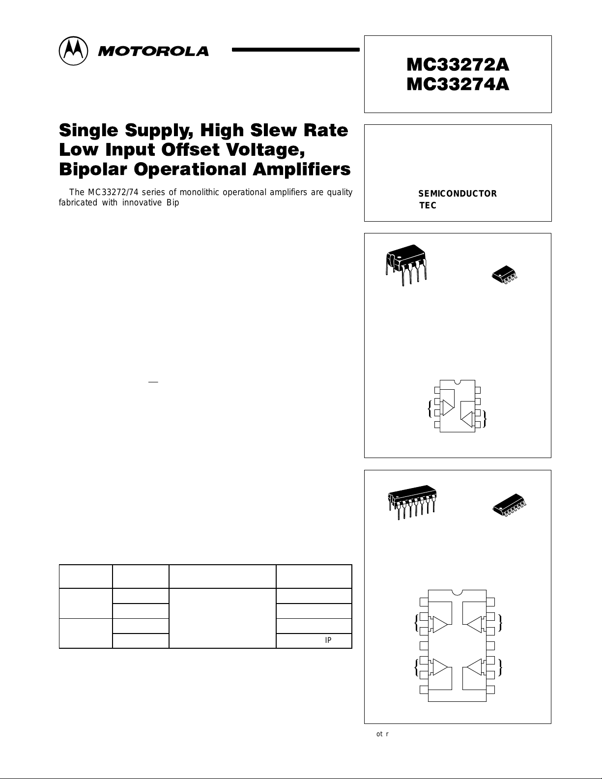
SEMICONDUCTOR
TECHNICAL DATA
8
1
P SUFFIX
PLASTIC PACKAGE
CASE 626
PIN CONNECTIONS
1
Output 1 V
Inputs 1
14
1
P SUFFIX
PLASTIC PACKAGE
CASE 646
2
3
4
V
EE
PIN CONNECTIONS
1
Output 1
2
Inputs 1
V
Inputs 2
Output 2
–
+
3
4
CC
5
+
–
6
78
DUAL
PLASTIC PACKAGE
8
7
–
+
(Top View)
6
–
+
5
Output 2
QUAD
PLASTIC PACKAGE
–
+
4
1
+
23
–
8
1
D SUFFIX
CASE 751
(SO–8)
CC
Inputs 2
14
1
D SUFFIX
CASE 751A
(SO–14)
14
Output 4
13
Inputs 4
12
11
V
EE
10
Inputs 3
9
Output 3
MOTOROLA ANALOG IC DEVICE DATA
(Top View)
Motorola, Inc. 1996 Rev 0
1
MC33272A MC33274A
MAXIMUM RATINGS
Rating Symbol Value Unit
Supply Voltage VCC to V
Input Differential Voltage Range V
Input Voltage Range V
Output Short Circuit Duration (Note 2) t
Maximum Junction Temperature T
Storage Temperature T
Maximum Power Dissipation P
NOTES: 1. Either or both input voltages should not exceed VCC or VEE.
2.Power dissipation must be considered to ensure maximum junction temperature
(TJ) is not exceeded (see Figure 2).
EE
IDR
IR
SC
J
stg
D
+36 V
(Note 1) V
(Note 1) V
Indefinite sec
+150 °C
–60 to +150 °C
(Note 2) mW
DC ELECTRICAL CHARACTERISTICS (V
Characteristics Figure Symbol Min Typ Max Unit
Input Offset Voltage (RS = 10 Ω, VCM = 0 V, VO = 0 V)
(VCC = +15 V, VEE = –15 V)
TA = +25°C
TA = –40° to +85°C
(VCC = 5.0 V, VEE = 0)
TA = +25°C
Average Temperature Coefficient of Input Offset Voltage
RS = 10 Ω, VCM = 0 V, VO = 0 V, TA = –40° to +85°C
Input Bias Current (VCM = 0 V, VO = 0 V)
TA = +25°C
TA = –40° to +85°C
Input Offset Current (VCM = 0 V, VO = 0 V)
TA = +25°C
TA = –40° to +85°C
Common Mode Input Voltage Range (∆VIO = 5.0 mV, VO = 0 V)
TA = +25°C
Large Signal Voltage Gain (VO = 0 V to 10 V, RL = 2.0 kΩ)
TA = +25°C
TA = –40° to +85°C
Output Voltage Swing (VID = ±1.0 V)
(VCC = +15 V, VEE = –15 V)
RL = 2.0 kΩ
RL = 2.0 kΩ
RL = 10 kΩ
RL = 10 kΩ
(VCC = 5.0 V, VEE = 0 V)
RL = 2.0 kΩ
RL = 2.0 kΩ
Common Mode Rejection (Vin = +13.2 V to –15 V) 13 CMR 80 100 — dB
Power Supply Rejection
VCC/VEE = +15 V/ –15 V, +5.0 V/ –15 V, +15 V/ –5.0 V
Output Short Circuit Current (VID = 1.0 V , Output to Ground)
Source
Sink
Power Supply Current Per Amplifier (VO = 0 V)
(VCC = +15 V, VEE = –15 V)
TA = +25°C
TA = –40° to +85°C
(VCC = 5.0 V, VEE = 0 V)
TA = +25°C
= +15 V, VEE = –15 V, TA = 25°C, unless otherwise noted.)
CC
3 |VIO|
—
—
—
3 ∆VIO/∆T
4, 5 I
|IIO|
6 V
7 A
8, 9, 12
10, 11
14, 15 PSR
16 I
17 I
VOL
VO+
VO–
VO+
VO–
V
V
CC
IB
ICR
OL
OH
SC
— 2.0 —
—
—
—
—
90
86
13.4
—
13.4
—
—
3.7
80 105 —
+25
–25
—
—
—
0.1
—
—
300
—
3.0
—
VEE to (VCC –1.8)
100
—
13.9
–13.9
14
–14.7
—
—
+37
–37
2.15
—
—
1.0
1.8
2.0
650
800
65
80
—
—
—
–13.5
—
–14.1
0.2
5.0
—
—
2.75
3.0
2.75
mV
µV/°C
nA
nA
V
dB
V
dB
mA
mA
2
MOTOROLA ANALOG IC DEVICE DATA
MC33272A MC33274A
AC ELECTRICAL CHARACTERISTICS (V
Characteristics Figure Symbol Min Typ Max Unit
Slew Rate
(Vin = –10 V to +10 V, RL = 2.0 kΩ, CL = 100 pF, AV = +1.0 V)
Gain Bandwidth Product (f = 100 kHz) 19 GBW 17 24 — MHz
AC Voltage Gain (RL = 2.0 kΩ, VO = 0 V, f = 20 kHz) 20, 21, 22 A
Unity Gain Frequency (Open Loop) f
Gain Margin (RL = 2.0 kΩ, CL = 0 pF) 23, 24, 26 A
Phase Margin (RL = 2.0 kΩ, CL = 0 pF) 23, 25, 26 φ
Channel Separation (f = 20 Hz to 20 kHz) 27 CS — –120 — dB
Power Bandwidth (VO = 20 V
Total Harmonic Distortion
(RL = 2.0 kΩ, f = 20 Hz to 20 kHz, VO = 3.0 V
Open Loop Output Impedance (VO = 0 V, f = 6.0 MHz) 29 |ZO| — 35 — Ω
Differential Input Resistance (VCM = 0 V) R
Differential Input Capacitance (VCM = 0 V) C
Equivalent Input Noise Voltage (RS = 100 Ω, f = 1.0 kHz) 30 e
Equivalent Input Noise Current (f = 1.0 kHz) 31 i
= 2.0 kΩ, THD ≤ 1.0%) BW
pp, RL
= +15 V, VEE = –15 V, TA = 25°C, unless otherwise noted.)
CC
18, 33 SR 8.0 10 — V/µs
— 65 — dB
— 5.5 — MHz
— 12 — dB
— 55 — Degrees
— 160 — kHz
— 16 — MΩ
— 3.0 — pF
— 18 —
— 0.5 —
, AV = +1.0)
rms
VO
U
m
m
P
28 THD — 0.003 — %
IN
IN
n
n
nV/ Hz√
pA/ Hz√
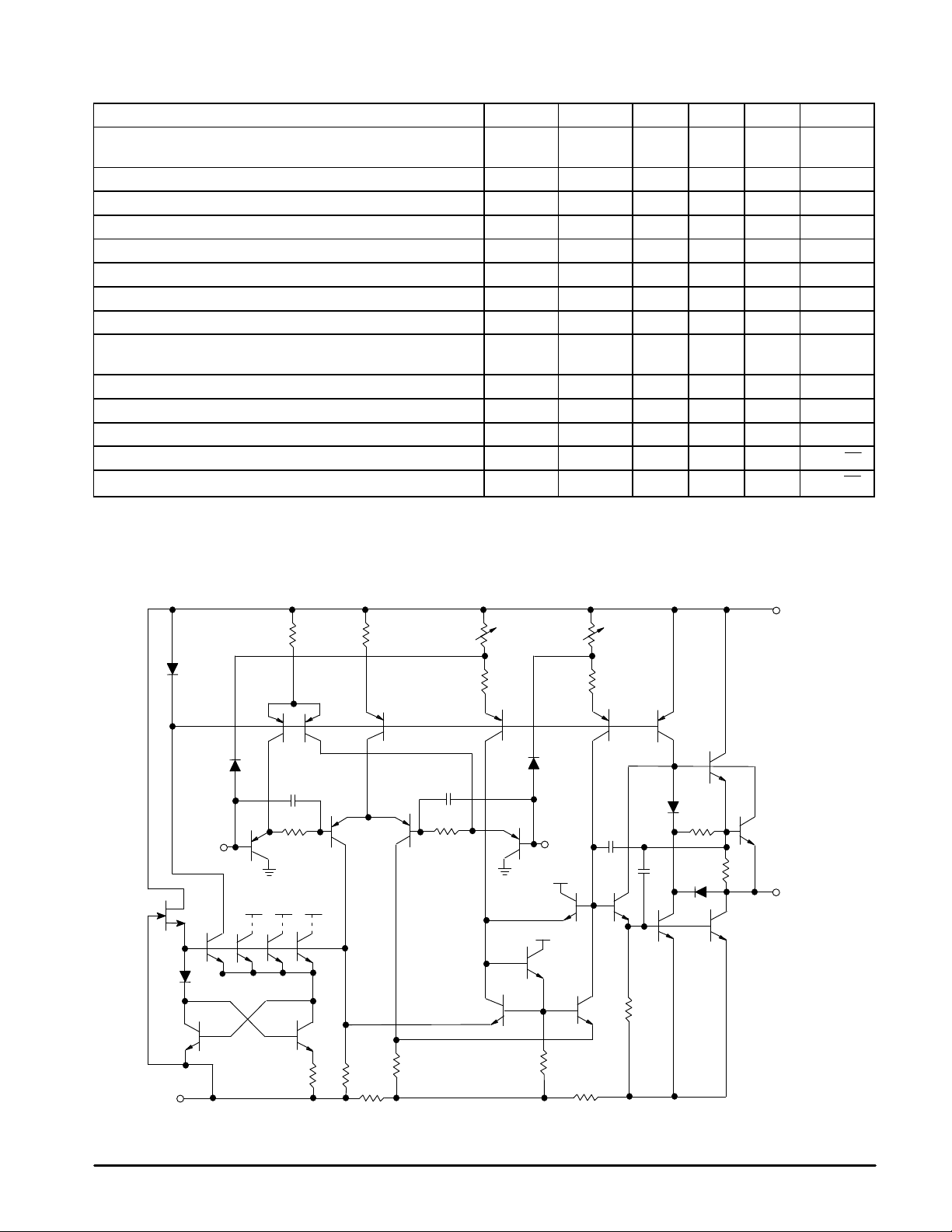
Figure 1. Equivalent Circuit Schematic
(Each Amplifier)
V
CC
–
V
in
+
V
in
+
Sections
BCD
V
O
+
V
EE
MOTOROLA ANALOG IC DEVICE DATA
3
MC33272A MC33274A
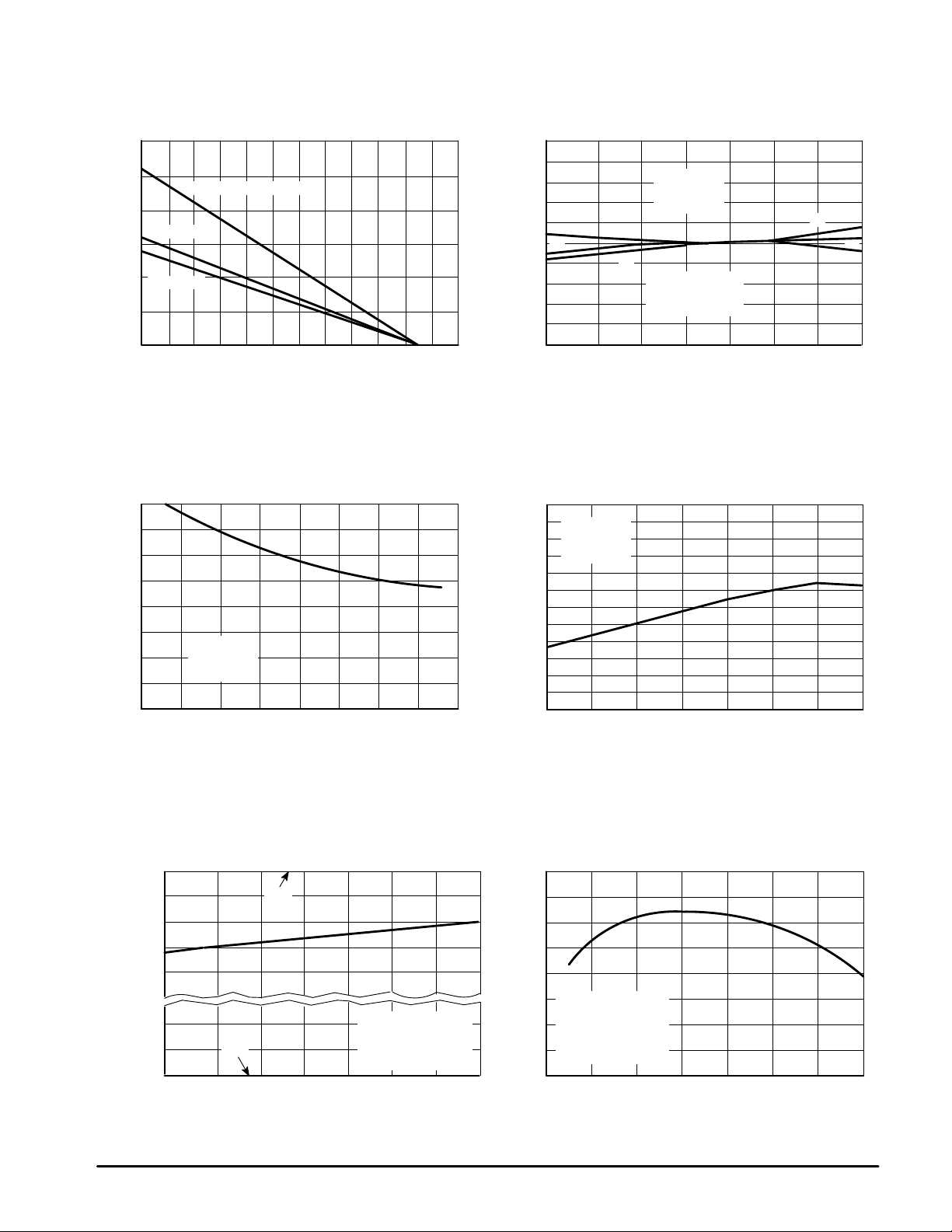
Figure 2. Maximum Power Dissipation
versus T emperature
2400
2000
1600
1200
800
400
0
D
P (MAX), MAXIMUM POWER DISSIPATION (mW)
MC33272P & MC33274P
MC33274D
MC33272D
0 20 40 60 80 100 120 140 160 180–60 –40 –20
TA, AMBIENT TEMPERATURE (°C)
Figure 4. Input Bias Current versus
Common Mode V oltage
400
350
300
250
200
150
100
IB
I , INPUT BIAS CURRENT (nA)
50
0
–16 –12 –8.0 –4.0 0 4.0 8.0 12 16
VCC = +15 V
VEE = –15 V
°
C
TA = 25
VCM, COMMON MODE VOLTAGE (V)
Figure 3. Input Offset Voltage versus
Temperature for Typical Units
5.0
3.0
1.0
2
–1.0
–3.0
IO
V , INPUT OFFSET VOLTAGE (mV)
–5.0
–55 –25 0 25 50 75 100 125
1
VCC = +15 V
VEE = –15 V
VCM = 0 V
3
°
1. VIO > 0 @ 25
2. VIO = 0 @ 25
3. VIO < 0 @ 25
TA, AMBIENT TEMPERATURE (°C)
C
°
C
°
C
1
Figure 5. Input Bias Current
versus T emperature
600
VCC = +15 V
500
VEE = –15 V
VCM = 0 V
400
300
200
100
IB
I , INPUT BIAS CURRENT (nA)
0
–55 –25 0 25 50 75 100 125
TA, AMBIENT TEMPERATURE (
°
C)
3
2
V
CC
VCC –0.5
VCC –1.0
VCC –1.5
VCC –2.0
VEE +1.0
VEE +0.5
ICR
V
EE
V , INPUT COMMON MODE VOLTAGE RANGE (V)
–55 –25 0 25 50 75 100 125
4
Figure 6. Input Common Mode V oltage
Range versus T emperature
V
CC
VCC = +5.0 V to +18 V
V
EE
TA, AMBIENT TEMPERATURE (
VEE = –5.0 V to –18 V
∆
VIO = 5.0 mV
VO = 0 V
°
C)
Figure 7. Open Loop Voltage Gain
versus T emperature
180
160
140
VCC = +15 V
VEE = –15 V
120
100
VOL
A , OPEN LOOP VOL TAGE GAIN (X 1.0 kV/V)
–55 –25 0 25 50 75 100 125
Ω
RL = 2.0 k
f = 10 Hz
∆
VO = –10 V to +10 V
TA, AMBIENT TEMPERATURE (°C)
MOTOROLA ANALOG IC DEVICE DATA
 Loading...