

T
40° t
125°C
查询MC33269D-12供应商
Order this document by MC33269/D
The MC33269 series are low dropout, medium current, fixed and
adjustable, positive voltage regulators specifically designed for use in low
input voltage applications. These devices offer the circuit designer an
economical solution for precision voltage regulation, while keeping power
losses to a minimum.
The regulator consists of a 1.0 V dropout composite PNP–NPN pass
transistor, current limiting, and thermal shutdown.
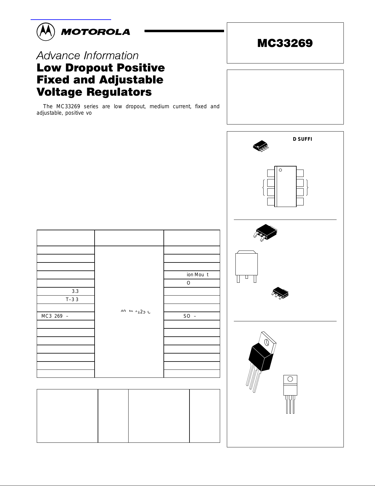
• 3.3 V, 5.0 V, 12 V and Adjustable Versions
• Space Saving DPAK, SOP–8 and SOT–223 Power Packages
• 1.0 V Dropout
• Output Current in Excess of 800 mA
• Thermal Protection
• Short Circuit Protection
• Output Trimmed to 1.0% Tolerance
• No Minimum Load Requirement for Fixed Voltage Output Devices
ORDERING INFORMATION
Operating
Device
MC33269D
MC33269DT
MC33269ST
MC33269T
MC33269D–3.3
MC33269DT–3.3
MC33269ST–3.3
MC33269T–3.3
MC33269D–5.0
MC33269DT–5.0 DPAK
MC33269T–5.0 Insertion Mount
MC33269ST–5.0 SOT–223
MC33269D–12 SOP–8
MC33269DT–12 DPAK
MC33269T–12 Insertion Mount
MC33269ST–12 SOT–223
DEVICE TYPE/NOMINAL OUTPUT VOLTAGE
MC33269D Adj MC33269D–5.0 5.0 V
MC33269DT Adj MC33269DT–5.0 5.0 V
MC33269T Adj MC33269T–5.0 5.0 V
MC33269ST Adj MC33269ST–5.0 5.0 V
MC33269D–3.3 3.3 V MC33269D–12 12 V
MC33269DT–3.3 3.3 V MC33269DT–12 12 V
MC33269T–3.3 3.3 V MC33269T–12 12 V
MC33269ST–3.3 3.3 V MC33269ST–12 12 V
Temperature Range
J
= –
°
o +
°
Package
SOP–8
DPAK
SOT–223
Insertion Mount
SOP–8
DPAK
SOT–223
Insertion Mount
SOP–8
800 mA
LOW DROPOUT
THREE–TERMINAL
VOLTAGE REGULATORS
D SUFFIX
8
1
Gnd/Adj
V
out
V
in
1
3
123
(Top View)
Heatsink surface (shown as terminal 4 in
case outline drawing) is connected to Pin 2.
1
2
3
Heatsink surface (shown as terminal 4 in
case outline drawing) is connected to Pin 2.
PLASTIC PACKAGE
1
2
3
4
(Top View)
PLASTIC PACKAGE
1. Gnd/Adj
2. V
out
3. V
in
PLASTIC PACKAGE
1
3
PLASTIC PACKAGE
123
(Top View)
CASE 751
(SOP–8)
NC
8
7
V
6
NC
5
DT SUFFIX
CASE 369A
(DPAK)
ST SUFFIX
CASE 318E
(SOT–223)
T SUFFIX
CASE 221A
Pin: 1. Gnd/Adj
out
2. V
3. V
out
in
This document contains information on a new product. Specifications and information herein
are subject to change without notice.
MOTOROLA ANALOG IC DEVICE DATA
Motorola, Inc. 1997 Rev 4
1
MAXIMUM RATINGS
Rating Symbol Value Unit
Power Supply Input Voltage V
Power Dissipation
Case 369A (DPAK)
TA = 25°C P
Thermal Resistance, Junction–to–Ambient θ
Thermal Resistance, Junction–to–Case θ
Case 751 (SOP–8)
TA = 25°C P
Thermal Resistance, Junction–to–Ambient θ
Thermal Resistance, Junction–to–Case θ
Case 221A
TA = 25°C P
Thermal Resistance, Junction–to–Ambient θ
Thermal Resistance, Junction–to–Case θ
Case 318E
TA = 25°C P
Thermal Resistance, Junction–to–Ambient θ
Thermal Resistance, Junction–to–Case θ
Operating Junction Temperature Range T
Storage Temperature T
NOTE: ESD data available upon request.
MC33269
in
D
JA
JC
D
JA
JC
D
JA
JC
D
JA
JC
J
stg
20 V
Internally Limited W
92 °C/W
6.0 °C/W
Internally Limited W
160 °C/W
25 °C/W
Internally Limited W
65 °C/W
5.0 °C/W
Internally Limited W
245 °C/W
15 °C/W
–40 to +150 °C
–55 to +150 °C
ELECTRICAL CHARACTERISTICS (C
Characteristic
Output Voltage (I
3.3 Suffix (VCC = 5.3 V) 3.27 3.3 3.33
5.0 Suffix (VCC = 7.0 V) 4.95 5.0 5.05
12 Suffix (VCC = 14 V) 11.88 12 12.12
Output Voltage (Line, Load and Temperature) (Note 1) V
(1.25 V ≤ Vin – V
(1.35 V ≤ Vin – V
3.3 Suffix 3.23 3.3 3.37
5.0 Suffix 4.9 5.0 5.1
12 Suffix 11.76 12 12.24
Reference Voltage (I
Adjustable
Reference Voltage (Line, Load and Temperature) (Note 1) V
(1.25 V ≤ Vin – V
(1.35 V ≤ Vin – V
Adjustable
Line Regulation Reg
(I
= 10 mA, Vin = [V
out
Load Regulation (Vin = V
Dropout Voltage Vin–V
(I
= 500 mA) – 1.0 1.25
out
(I
= 800 mA) – 1.1 1.35
out
Ripple Rejection RR 55 – – dB
(10 Vpp, 120 Hz Sinewave; I
Current Limit (Vin – V
Quiescent Current (Fixed Output) I
Minimum Required Load Current I
Fixed Output – – 0
Adjustable 8.0 – –
Adjustment Pin Current I
NOTE 1: The MC33269–12, Vin – V
= 10 mA, TJ = 25°C) V
out
≤ 15 V , I
out
≤ 10 V , I
out
= 10 mA, Vin – V
out
≤ 15 V , I
out
≤ 10 V , I
out
out
out
= 10 V) I
out
= 500 mA)
out
= 800 mA)
out
= 500 mA)
out
= 800 mA)
out
+ 1.5 V] to Vin = 20 V, TJ = 25°C)
+ 3.0 V, I
= 500 mA)
out
is limited to 8.0 V maximum, because of the 20 V maximum rating applied to Vin.
out
= 10 µF, TA = 25°C, for min/max values TJ = –40°C to +125°C, unless otherwise noted.)
O
Symbol Min Typ Max Unit
O
O
= 2.0 V, TJ = 25°C) V
out
= 10 mA to 800 mA, TJ = 25°C) Reg
out
ref
ref
line
load
out
Limit
Q
Load
Adj
1.235 1.25 1.265 V
1.225 1.25 1.275 V
– – 0.3 %
– – 0.5 %
800 – – mA
– 5.5 8.0 mA
– – 120 µA
V
V
V
mA
2
MOTOROLA ANALOG IC DEVICE DATA
MC33269
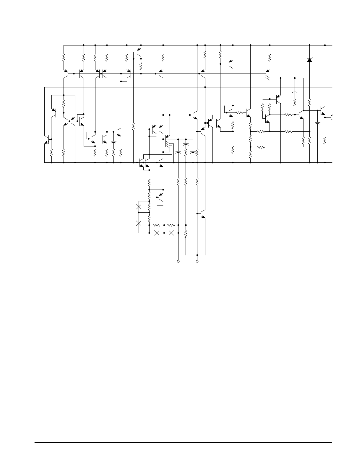
Internal Schematic
Trim Links
V
Adj Gnd
This device contains 38 active transistors.
MOTOROLA ANALOG IC DEVICE DATA
3

1.5
1.3
Figure 1. Dropout Voltage versus
Output Load Current
MC33269
Figure 2. Transient Load Regulation
TA = 25°C
1.1
0.9
, DROPOUT VOLTAGE (V)
out
0.7
–V
in
V
0.5
0 200 400 600 800 1000
IO, OUTPUT LOAD CURRENT (mA)
TA = –40°C
TA = 125°C
Figure 3. Dropout Voltage
versus T emperature
1100
IO = 800 mA
1060
1020
980
940
, OVERVOL TAGE INPUT THRESHOLD (%V )
900
–55
FB(OV) FB
V
–25 0 25 50 75 100 125
TA, AMBIENT TEMPERATURE (°C)
, OUTPUT
O
V
∆
VOLTAGE DEVIATIONCURRENT
, OUTPUTI
O
20 ms/DIV
Cin = 10 µF
µ
CO = 10
Vin = VO + 3.0 V
Preload = 0.1 A
F Tantalum
Figure 4. MC33269–XX Output DC Current versus
Input–Output Differential Voltage
1.6
1.4
1.2
OUTPUT CURRENT (A)
1.0
0.8
0.6
0.4
0.2
0
0
2.0 4.0 6.0 8.0 10 12 14 16
INPUT–OUTPUT VOLTAGE DIFFERENTIAL (V)
TA = 25°C
MC33269D–XX
L = 25 mm Copper
100
mV/Div
0.5 A
0 A
Figure 5. MC33269 Ripple Rejection
versus Frequency
70
VO = 3.3 V or 5.0 V
60
50
Vin = VO + 3.0 V
40
IL = 800 mA
TA = 25
30
RR, RIPPLE REJECTION RATIO (dB)
20
0.1 1.0 10 100
°
C
VO = 12 V
f, FREQUENCY (kHz)
4
70
60
50
40
30
RR, RIPPLE REJECTION RATIO (dB)
20
0.1
Figure 6. MC33269–ADJ Ripple Rejection
versus Frequency
Vin = 8.0 V
V
= 5.0 V
out
IL = 800 mA
C
TA = 25
Adj
= 22
°
C
µ
F
f, FREQUENCY (kHz)
MOTOROLA ANALOG IC DEVICE DATA
100101.0

MC33269
Figure 8. SOP–8 Thermal Resistance and Maximum
°
Power Dissipation versus P.C.B. Copper Length
170
150
130
JUNCTION–TO–AIR ( C/W)
110
90
70
50
30
02030504010
JA
θ
R , THERMAL RESIST ANCE,
R
θ
JA
L, LENGTH OF COPPER (mm)
P
for TA = 50°C
D(max)
Graph represents symmetrical layout
2.0 oz.
L
Copper
3.0 mmL
Figure 7. SOT–223 Thermal Resistance and Maximum
Power Dissipation versus P.C.B. Copper Length
280
240
°
200
160
Free Air
Mounted
Vertically
Minimum
Size Pad
3.2
2.8
2.4
2.0
1.6
1.2
0.8
0.4
°
100
JUNCTION–TO–AIR ( C/W)
JA
θ
R , THERMAL RESIST ANCE,
P
D(max)
Figure 9. DP AK Thermal Resistance and Maximum
Power Dissipation versus P.C.B. Copper Length
P
for TA = 50°C
Free Air
90
80
70
60
50
40
for TA = 50°C
Mounted
Vertically
010203025155.0
2.0 oz. Copper
L
Minimum
Size Pad
L
D(max)
2.0 oz. Copper
L
R
θ
JA
L, LENGTH OF COPPER (mm)
2.50
1.25
0.83
0.63
L
2.4
2.0
1.6
1.2
0.8
0.4
0
, MAXIMUM POWER DISSIPATION (W)
D
P
120
JA
JUNCTION-TO-AIR ( C/W)
θ
R , THERMAL RESISTANCE
80
40
010203025155.0
R
θ
JA
L, LENGTH OF COPPER (mm)
0.50
0.42
0.35
, MAXIMUM POWER DISSIPATION (W)
D
P
MOTOROLA ANALOG IC DEVICE DATA
5

MC33269
APPLICATIONS INFORMATION
Figures 10 through 14 are typical application circuits. The
output current capability of the regulator is in excess of
800 mA, with a typical dropout voltage of less than 1.0 V.
Internal protective features include current and thermal
limiting.
The MC33269 is not internally compensated and thus
requires an external output capacitor for stability. The
capacitor should be at least 10 µF with an equivalent series
resistance (ESR) of less than 10 Ω over the anticipated
operating temperature range. With economical electrolytic
capacitors, cold temperature operation can pose a problem.
As temperature decreases, the capacitance also decreases
and the ESR increases, which could cause the circuit to
oscillate. Solid tantalum capacitors may be a better choice if
small size is a requirement. Also capacitance and ESR of a
solid tantalum capacitor is more stable over temperature. An
input bypass capacitor is recommended to improve transient
response or if the regulator is connected to the supply input
Figure 10. T ypical Fixed Output Application
V
in
C
in
An input capacitor is not necessary for stability, however
it will improve the overall performance.
MC33269–XX
Gnd
C
10
V
out
O
µ
F
filter with long wire lengths. This will reduce the circuit’s
sensitivity to the input line impedance at high frequencies. A
0.33 µF or larger tantalum, mylar , ceramic, or other capacitor
having low internal impedance at high frequencies should be
chosen. The bypass capacitor should be mounted with
shortest possible lead or track length directly across the
regulator’s input terminals. Applications should be tested
over all operating conditions to insure stability .
Internal thermal limiting circuitry is provided to protect the
integrated circuit in the event that the maximum junction
temperature is exceeded. When activated, typically at 170°C,
the output is disabled. There is no hysteresis built into the
thermal limiting circuit. As a result, if the device is
overheating, the output will appear to be oscillating. This
feature is provided to prevent catastrophic failures from
accidental device overheating. It is not intended to be used
as a substitute for proper heatsinking.
Figure 11. Typical Adjustable Output Application
R1
R2
I
Adj
R2
V
out
C
O
10
µ
F
V
in
C
in
V
out
MC33269
Adj
C
Adj
+
1.25ǒ1
*
R2
Ǔ
)
)
R1
Figure 12. Current Regulator
1.25
R
S
R
V
in
C
in
MC33269
Adj
+
I
out
I
S
out
C
10
O
µ
F
Figure 13. Battery Backed–Up Power Supply
V
in
C
C
in
The Schottky diode in series with the ground leg of the upper
regulator shifts its output voltage higher by the forward
voltage drop of the diode. This will cause the lower device
to remain off until the input voltage is removed.
MC33269–XX
in
Gnd
MC33269–XX
Gnd
V
out
C
O
10 µF
*C
is optional, however it will improve the ripple rejection.
Adj
The MC34269 develops a 1.25 V reference voltage between the
output and the adjust terminal. Resistor R1, operates with
constant current to flow through it and resistor R2. This current
should be set such that the Adjust Pin current causes negligible
drop across resistor R2. The total current with minimum load
should be greater than 8.0 mA.
Figure 14. Digitally Controlled V oltage Regulator
R1
R2
V
C
10
out
O
µ
F
V
in
C
in
R2 sets the maximum output voltage. Each transistor
reduces the output voltage when turned on.
MC33269
Adj
6
MOTOROLA ANALOG IC DEVICE DATA

MC33269
OUTLINE DIMENSIONS
D SUFFIX
PLASTIC PACKAGE
CASE 751–05
(SOP–8)
ISSUE R
A
C
A1
D
58
0.25MB
E
1
B
e
H
4
M
h
X 45
_
q
C
A
SEATING
PLANE
0.10
L
B
SS
A0.25MCB
NOTES:
1. DIMENSIONING AND TOLERANCING PER ASME
Y14.5M, 1994.
2. DIMENSIONS ARE IN MILLIMETERS.
3. DIMENSION D AND E DO NOT INCLUDE MOLD
PROTRUSION.
4. MAXIMUM MOLD PROTRUSION 0.15 PER SIDE.
5. DIMENSION B DOES NOT INCLUDE MOLD
PROTRUSION. ALLOWABLE DAMBAR
PROTRUSION SHALL BE 0.127 TOTAL IN EXCESS
OF THE B DIMENSION AT MAXIMUM MATERIAL
CONDITION.
MILLIMETERS
DIM MIN MAX
A 1.35 1.75
A1 0.10 0.25
B 0.35 0.49
C 0.18 0.25
D 4.80 5.00
E
3.80 4.00
1.27 BSCe
H 5.80 6.20
h
0.25 0.50
L 0.40 1.25
0 7
q
__
DT SUFFIX
PLASTIC PACKAGE
CASE 369A–13
(DPAK)
ISSUE Y
NOTES:
SEATING
–T–
PLANE
B
V
S
R
4
A
123
K
F
L
D
2 PL
G
0.13 (0.005) T
C
E
Z
U
J
H
M
1. DIMENSIONING AND TOLERANCING PER ANSI
Y14.5M, 1982.
2. CONTROLLING DIMENSION: INCH.
DIM MIN MAX MIN MAX
A 0.235 0.250 5.97 6.35
B 0.250 0.265 6.35 6.73
C 0.086 0.094 2.19 2.38
D 0.027 0.035 0.69 0.88
E 0.033 0.040 0.84 1.01
F 0.037 0.047 0.94 1.19
G 0.180 BSC 4.58 BSC
H 0.034 0.040 0.87 1.01
J 0.018 0.023 0.46 0.58
K 0.102 0.114 2.60 2.89
L 0.090 BSC 2.29 BSC
R 0.175 0.215 4.45 5.46
S 0.020 0.050 0.51 1.27
U 0.020 ––– 0.51 –––
V 0.030 0.050 0.77 1.27
Z 0.138 ––– 3.51 –––
MILLIMETERSINCHES
MOTOROLA ANALOG IC DEVICE DATA
7

0.08 (0003)
Q
H
Z
MC33269
OUTLINE DIMENSIONS
ST SUFFIX
PLASTIC PACKAGE
A
F
4
S
123
B
D
L
G
C
H
B
4
F
T
A
123
K
U
L
V
G
D
N
CASE 318E–04
ISSUE H
(SOT–223)
M
T SUFFIX
PLASTIC PACKAGE
CASE 221A–06
ISSUE Y
–T–
C
S
R
J
SEATING
PLANE
NOTES:
1 DIMENSIONING AND TOLERANCING PER ANSI
Y14.5M, 1982.
2 CONTROLLING DIMENSION: INCH.
INCHES
DIMAMIN MAX MIN MAX
0.249 0.263 6.30 6.70
B 0.130 0.145 3.30 3.70
C 0.060 0.068 1.50 1.75
D 0.024 0.035 0.60 0.89
F 0.115 0.126 2.90 3.20
G 0.087 0.094 2.20 2.40
H 0.0008 0.0040 0.020 0.100
J
J 0.009 0.014 0.24 0.35
K 0.060 0.078 1.50 2.00
L 0.033 0.041 0.85 1.05
M 0 10 0 10
____
S 0.264 0.287 6.70 7.30
MILLIMETERS
K
NOTES:
1. DIMENSIONING AND TOLERANCING PER ANSI
Y14.5M, 1982.
2. CONTROLLING DIMENSION: INCH.
3. DIMENSION Z DEFINES A ZONE WHERE ALL
BODY AND LEAD IRREGULARITIES ARE
ALLOWED.
DIM MIN MAX MIN MAX
A 0.570 0.620 14.48 15.75
B 0.380 0.405 9.66 10.28
C 0.160 0.190 4.07 4.82
D 0.025 0.035 0.64 0.88
F 0.142 0.147 3.61 3.73
G 0.095 0.105 2.42 2.66
H 0.110 0.155 2.80 3.93
J 0.018 0.025 0.46 0.64
K 0.500 0.562 12.70 14.27
L 0.045 0.060 1.15 1.52
N 0.190 0.210 4.83 5.33
Q 0.100 0.120 2.54 3.04
R 0.080 0.110 2.04 2.79
S 0.045 0.055 1.15 1.39
T 0.235 0.255 5.97 6.47
U 0.000 0.050 0.00 1.27
V 0.045 ––– 1.15 –––
Z ––– 0.080 ––– 2.04
MILLIMETERSINCHES
Motorola reserves the right to make changes without further notice to any products herein. Motorola makes no warranty , representation or guarantee regarding
the suitability of its products for any particular purpose, nor does Motorola assume any liability arising out of the application or use of any product or circuit, and
specifically disclaims any and all liability, including without limitation consequential or incidental damages. “T ypical” parameters which may be provided in Motorola
data sheets and/or specifications can and do vary in different applications and actual performance may vary over time. All operating parameters, including “Typicals”
must be validated for each customer application by customer’s technical experts. Motorola does not convey any license under its patent rights nor the rights of
others. Motorola products are not designed, intended, or authorized for use as components in systems intended for surgical implant into the body, or other
applications intended to support or sustain life, or for any other application in which the failure of the Motorola product could create a situation where personal injury
or death may occur. Should Buyer purchase or use Motorola products for any such unintended or unauthorized application, Buyer shall indemnify and hold Motorola
and its officers, employees, subsidiaries, affiliates, and distributors harmless against all claims, costs, damages, and expenses, and reasonable attorney fees
arising out of, directly or indirectly, any claim of personal injury or death associated with such unintended or unauthorized use, even if such claim alleges that
Motorola was negligent regarding the design or manufacture of the part. Motorola and are registered trademarks of Motorola, Inc. Motorola, Inc. is an Equal
Opportunity/Affirmative Action Employer.
How to reach us:
USA/EUROPE/Locations Not Listed: Motorola Literature Distribution; JAPAN: Nippon Motorola Ltd.: SPD, Strategic Planning Office, 4–32–1,
P.O. Box 5405, Denver, Colorado 80217. 303–675–2140 or 1–800–441–2447 Nishi–Gotanda, Shinagawa–ku, Tokyo 141, Japan. 81–3–5487–8488
Mfax: RMFAX0@email.sps.mot.com – TOUCHTONE 602–244–6609 ASIA/PACIFIC: Motorola Semiconductors H.K. Ltd.; 8B Tai Ping Industrial Park,
INTERNET: http://motorola.com/sps
8
– US & Canada ONLY 1–800–774–1848 51 Ting Kok Road, T a i Po, N.T., Hong Kong. 852–26629298
◊
MOTOROLA ANALOG IC DEVICE DATA
Mfax is a trademark of Motorola, Inc.
MC33269/D
 Loading...