

MOTOROLA MC33267TV, MC33267D2TR4, MC33267TH Datasheet
SEMICONDUCTOR
TECHNICAL DATA
LOW DROPOUT
REGULATOR with
POWER–UP RESET
Order this document by MC33267/D
1
5
T SUFFIX
PLASTIC PACKAGE
CASE 314D
TV SUFFIX
PLASTIC PACKAGE
CASE 314B
1
Pin 1. VCC Input
2. Reset
3. Ground
4. Delay
5. Output
Heatsink surface connected to Pin 3.
5
D2T SUFFIX
PLASTIC PACKAGE
CASE 936A
(D2PAK)
Heatsink surface (shown as
terminal 6 in case outline
drawing) is connected to Pin 3.
1
5
1
MOTOROLA ANALOG IC DEVICE DATA
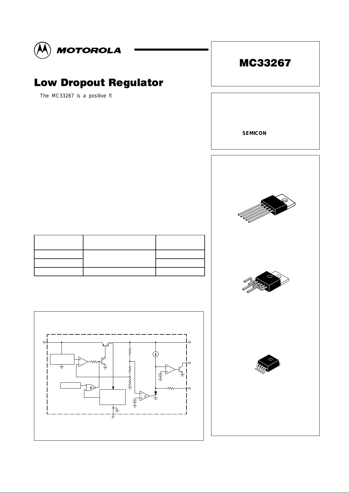
The MC33267 is a positive fixed 5.0 V regulator that is specifically
designed to maintain proper voltage regulation with an extremely low
input–to–output voltage differential. This device is capable of supplying
output currents in excess of 500 mA and contains internal current limiting and
thermal shutdown protection. Also featured is an on–chip power–up reset
circuit that is ideally suited for use in microprocessor based systems.
Whenever the regulator output voltage is below nominal, the reset output is
held low. A programmable time delay is initiated after the regulator has
reached its nominal level and upon timeout, the reset output is released.
Due to the low dropout voltage specifications, the MC33267 is ideally
suited for use in battery powered industrial and consumer equipment where
an extension of useful battery life is desirable. This device is contained in an
economical five lead TO–220 type package.
• Low Input–to–Output Voltage Differential
• Output Current in Excess of 500 mA
• On–Chip Power–Up Reset Circuit with Programmable Delay
• Internal Current Limiting with Thermal Shutdown
• Economical Five Lead TO–220 Type Packages
ORDERING INFORMATION
Device
Tested Operating
Temperature Range
Package
MC33267T
–
°
°
Plastic Power
MC33267TV
T
J
= –
40 ° to +125°C
Plastic Power
MC33267D2T TJ = –40 ° to +105°C Surface Mount
Representative Block Diagram
Input Output
1
5
Reference
1.25 V
Thermal
Overcurrent
Detector
Ground 3
1.25 V
Delay
R
0.03
R
3.01
R
20
µ
A
3.8 V
Reset
200
Reset
2
Delay
4
+
+
This device contains 37 active transistors.
Motorola, Inc. 1996 Rev 1
MC33267
2
MOTOROLA ANALOG IC DEVICE DATA
MAXIMUM RATINGS
Rating Symbol Value Unit
Input Voltage Range V
in
– 20 to + 40 Vdc
Delay Voltage Range V
DLYR
– 0.3 to V
O
V
Delay Sink Current I
DLY(sink)
25 mA
Reset Voltage Range V
RR
– 0.3 to +15 V
Reset Sink Current I
R(sink)
50 mA
Power Dissipation
Case 314B and 314D (TO–220 Type)
TA = 25°C
Thermal Resistance, Junction–to–Ambient
Thermal Resistance, Junction–to–Case
Case 936A (D2PAK) [Note 1]
TA = 90°C
Thermal Resistance, Junction–to–Ambient
Thermal Resistance, Junction–to–Case
P
D
R
θJA
R
θJC
P
D
R
θJA
R
θJC
Internally Limited
62.5
4.0
Internally Limited
70
5.0
W
°C/W
°C/W
W
°C/W
°C/W
Operating Junction Temperature Range T
J
–40 to +150 °C
Storage Temperature Range T
stg
–55 to +150 °C
NOTE: 1.D2PAK Junction–to–Ambient Thermal Resistance is for vertical mounting. Refer to Figure 7
for board mounted thermal resistance.
ELECTRICAL CHARACTERISTICS (V
in
= 14.4 V, IO = 5.0 mA , CO = 100 µF, C
O(ESR)
≤ 0.3 Ω , TJ = 25°C (Note 2), unless otherwise noted.)
Characteristic
Symbol Min Typ Max Unit
Output Voltage (IO = 5.0 mA to 500 mA, Vin = 6.0 V to 28 V)
TJ = 25°C
TJ = – 40° to +125°C
V
O
4.95
4.9
5.05
–
5.15
5.2
V
Line Regulation (Vin = 6.0 V to 26 V) Reg
line
– 3.0 50 mV
Load Regulation (IO = 5.0 mA to 500 mA) Reg
load
– 1.0 50 mV
Bias Current
IO = 0 mA
IO = 150 mA
IO = 500 mA
IO = 500 mA, Vin = 6.2 V
I
B
–
–
–
–
12
22
100
120
20
40
200
300
mA
Ripple Rejection (f = 120 Hz, Vin = 7.0 V to 17 V,
IO = 350 mA, CO = 100 µF)
RR
60 80 –
dB
Dropout Voltage (IO = 500 mA) Vin – V
O
– 0.58 0.8 V
Delay Comparator Threshold (VO Decreasing) V
th(DLY)
4.8 VO– 0.15 VO– 0.08 V
Delay Pin Source Current I
DLY(source)
12 20 28 µA
Reset Comparator Threshold V
th(R)
3.6 3.8 4.0 V
Reset Sink Saturation (I
sink
= 10 mA) V
CE(sat)
– 0.2 0.8 V
Reset Off–State Leakage (VCE = 5.0 V) I
R(leak)
– 0.3 10 µA
NOTE: 2. Low duty cycle pulse techniques are used during test to maintain junction temperature as close to ambient as possible.
MC33267
3
MOTOROLA ANALOG IC DEVICE DATA
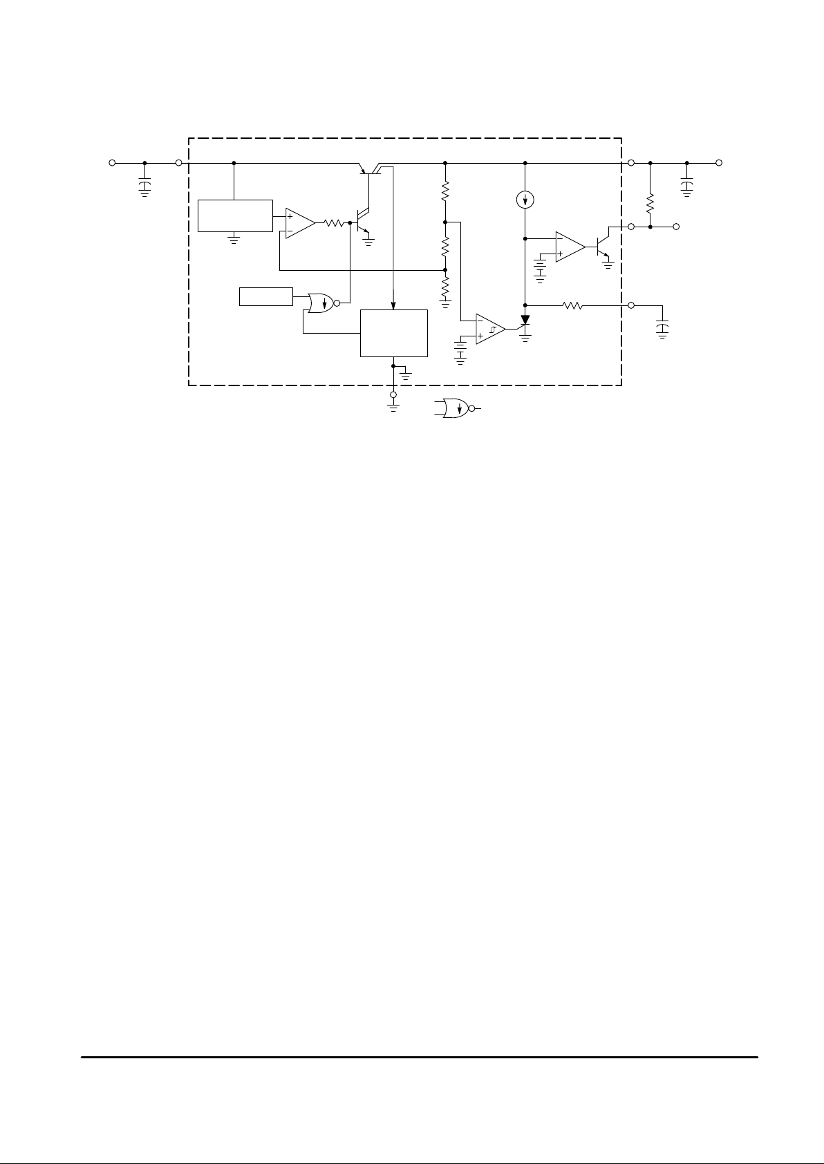
+
0.1
Figure 1. Typical Application Circuit
Input Output
1 5
Reference
1.25 V
Thermal
Overcurrent
Detector
Ground 3
1.25 V
Delay
R
0.03
R
3.01
R
20
µ
A
3.8 V
Reset
200
Reset
Output
2
Delay
4
+
+
+
C
in
V
in
100C
O
V
O
C
DLY
+
Sink Only
Positive True Logic
=
APPLICATION CIRCUIT INFORMATION
The MC33267 is a low dropout, positive fixed 5.0 V,
500 mA regulator. Protection features include output current
limiting and thermal shutdown. System protection consists of
an on–chip power–up microprocessor reset circuit.
A typical applications circuit is shown in Figure 1. The input
bypass capacitor (Cin) is recommended if the regulator is
located an appreciable distance (≥ 4″) from the supply input
filter. This will reduce the circuit’s sensitivity to the input line
impedance at high frequencies.
These regulators are not internally compensated and thus
require an external output capacitor (CO) for stability. The
recommended capacitance is 100 µF with an equivalent
series resistance (ESR) of less than 0.3 Ω. A minimum
capacitance of 33 µF with a maximum ESR of 3.0 Ω can be
used in applications where space is a premium, however,
these limits must be observed over the entire operating
temperature range of the regulator circuit.
With economical electrolytic capacitors, cold temperature
operation can pose a serious stability problem. As the
electrolyte freezes, around – 30°C, the capacitance will
decrease and the ESR will increase drastically, causing the
circuit to oscillate. Quality electrolytic capacitors with
extended temperature ranges of – 40°C to + 85°C and
–55°C to +105°C are readily available. It is suggested that
oven testing of the entire circuit be performed with maximum
load, minimum input voltage, and minimum ambient
temperature.
Figure 2 shows the reset circuit timing relationship. Note
that whenever the regulator’s output is less than 4.9 V, the
delay capacitor (C
DLY
) is immediately discharged, and the
reset output is held in a low state. As the regulator’s output
voltage increases beyond 4.97 V, the delay comparator will
allow the 20 µA current source to charge C
DLY
. The reset
output will go to a high state when C
DLY
crosses the 3.8 V
threshold of the reset comparator. The reset delay time is
controlled by the value selected for C
DLY
. The required
system reset time is governed by the microprocessor and
usually a reset signal which lasts several machine cycles is
sufficient.
 Loading...