

T
40 ° to +125°C
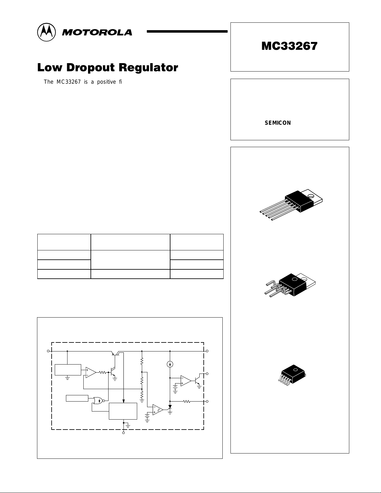
The MC33267 is a positive fixed 5.0 V regulator that is specifically
designed to maintain proper voltage regulation with an extremely low
input–to–output voltage differential. This device is capable of supplying
output currents in excess of 500 mA and contains internal current limiting and
thermal shutdown protection. Also featured is an on–chip power–up reset
circuit that is ideally suited for use in microprocessor based systems.
Whenever the regulator output voltage is below nominal, the reset output is
held low. A programmable time delay is initiated after the regulator has
reached its nominal level and upon timeout, the reset output is released.
Due to the low dropout voltage specifications, the MC33267 is ideally
suited for use in battery powered industrial and consumer equipment where
an extension of useful battery life is desirable. This device is contained in an
economical five lead TO–220 type package.
• Low Input–to–Output Voltage Dif ferential
• Output Current in Excess of 500 mA
• On–Chip Power–Up Reset Circuit with Programmable Delay
• Internal Current Limiting with Thermal Shutdown
• Economical Five Lead TO–220 T ype Packages
ORDERING INFORMATION
Tested Operating
Device
MC33267T
MC33267TV
MC33267D2T TJ = –40 ° to +105°C Surface Mount
Temperature Range
–
J
= –
°
°
Package
Plastic Power
Plastic Power
Order this document by MC33267/D
LOW DROPOUT
REGULATOR with
POWER–UP RESET
SEMICONDUCTOR
TECHNICAL DATA
Pin 1. VCC Input
2. Reset
3. Ground
4. Delay
5. Output
1
5
T SUFFIX
PLASTIC PACKAGE
CASE 314D
1
Representative Block Diagram
Input Output
1
Reference
1.25 V
Thermal
Overcurrent
Ground 3
This device contains 37 active transistors.
Detector
3.01
0.03
µ
A
20
R
Reset
R
R
Delay
+
1.25 V
+
3.8 V
200
MOTOROLA ANALOG IC DEVICE DATA
5
Reset
2
Delay
4
5
TV SUFFIX
PLASTIC PACKAGE
CASE 314B
Heatsink surface connected to Pin 3.
1
5
D2T SUFFIX
PLASTIC PACKAGE
CASE 936A
(D2PAK)
Heatsink surface (shown as
terminal 6 in case outline
drawing) is connected to Pin 3.
Motorola, Inc. 1996 Rev 1
1
MC33267
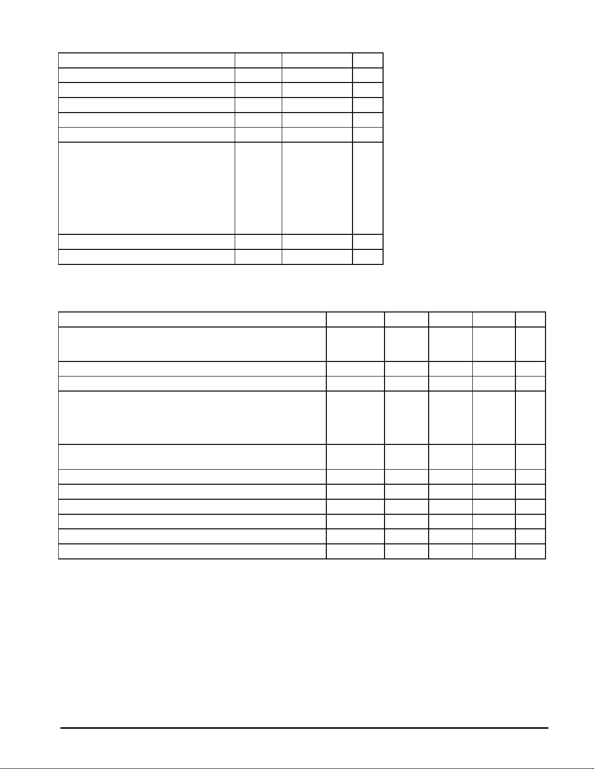
MAXIMUM RATINGS
Rating Symbol Value Unit
Input Voltage Range V
Delay Voltage Range V
Delay Sink Current I
Reset Voltage Range V
Reset Sink Current I
Power Dissipation
Case 314B and 314D (TO–220 Type)
TA = 25°C
Thermal Resistance, Junction–to–Ambient
Thermal Resistance, Junction–to–Case
Case 936A (D2PAK) [Note 1]
TA = 90°C
Thermal Resistance, Junction–to–Ambient
Thermal Resistance, Junction–to–Case
Operating Junction Temperature Range T
Storage Temperature Range T
NOTE: 1.D2PAK Junction–to–Ambient Thermal Resistance is for vertical mounting. Refer to Figure 7
for board mounted thermal resistance.
in
DLYR
DLY(sink)
RR
R(sink)
P
D
R
θJA
R
θJC
P
D
R
θJA
R
θJC
J
stg
– 20 to + 40 Vdc
– 0.3 to V
– 0.3 to +15 V
Internally Limited
Internally Limited
–40 to +150 °C
–55 to +150 °C
O
25 mA
50 mA
62.5
4.0
70
5.0
°C/W
°C/W
°C/W
°C/W
V
W
W
ELECTRICAL CHARACTERISTICS (V
Characteristic
Output Voltage (IO = 5.0 mA to 500 mA, Vin = 6.0 V to 28 V)
TJ = 25°C
TJ = – 40° to +125°C
Line Regulation (Vin = 6.0 V to 26 V) Reg
Load Regulation (IO = 5.0 mA to 500 mA) Reg
Bias Current
IO = 0 mA
IO = 150 mA
IO = 500 mA
IO = 500 mA, Vin = 6.2 V
Ripple Rejection (f = 120 Hz, Vin = 7.0 V to 17 V,
IO = 350 mA, CO = 100 µF)
Dropout Voltage (IO = 500 mA) Vin – V
Delay Comparator Threshold (VO Decreasing) V
Delay Pin Source Current I
Reset Comparator Threshold V
Reset Sink Saturation (I
Reset Off–State Leakage (VCE = 5.0 V) I
NOTE: 2. Low duty cycle pulse techniques are used during test to maintain junction temperature as close to ambient as possible.
= 10 mA) V
sink
= 14.4 V, IO = 5.0 mA , CO = 100 µF, C
in
≤ 0.3 Ω, TJ = 25°C (Note 2), unless otherwise noted.)
O(ESR)
Symbol Min Typ Max Unit
V
O
line
load
I
B
RR
O
th(DLY)
DLY(source)
th(R)
CE(sat)
R(leak)
4.95
4.9
– 3.0 50 mV
– 1.0 50 mV
–
–
–
–
60 80 –
– 0.58 0.8 V
4.8 VO– 0.15 VO– 0.08 V
12 20 28 µA
3.6 3.8 4.0 V
– 0.2 0.8 V
– 0.3 10 µA
5.05
–
12
22
100
120
5.15
V
5.2
mA
20
40
200
300
dB
2
MOTOROLA ANALOG IC DEVICE DATA
MC33267
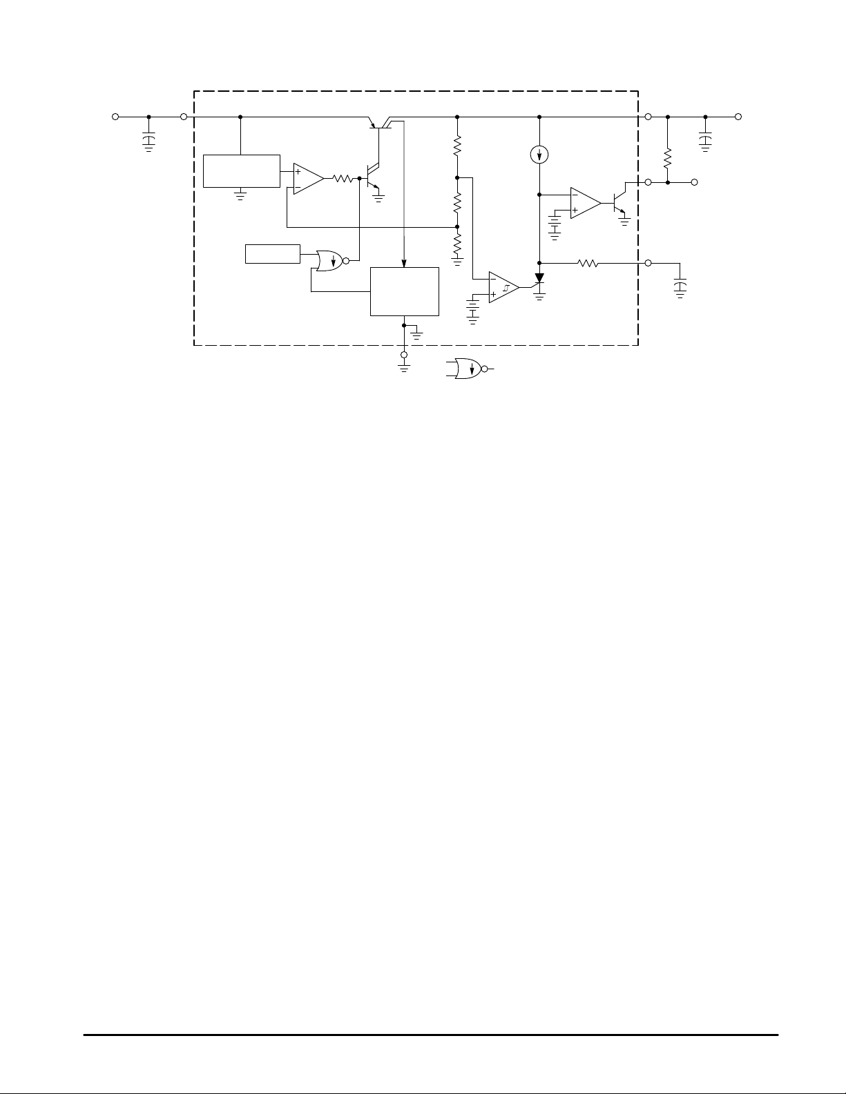
Figure 1. T ypical Application Circuit
V
in
C
Input Output
+
1 5
0.1
in
Reference
1.25 V
Thermal
Overcurrent
Detector
Ground 3
APPLICATION CIRCUIT INFORMATION
The MC33267 is a low dropout, positive fixed 5.0 V,
500 mA regulator. Protection features include output current
limiting and thermal shutdown. System protection consists of
an on–chip power–up microprocessor reset circuit.
A typical applications circuit is shown in Figure 1. The input
bypass capacitor (Cin) is recommended if the regulator is
located an appreciable distance (≥ 4″) from the supply input
filter. This will reduce the circuit’s sensitivity to the input line
impedance at high frequencies.
These regulators are not internally compensated and thus
require an external output capacitor (CO) for stability. The
recommended capacitance is 100 µF with an equivalent
series resistance (ESR) of less than 0.3 Ω. A minimum
capacitance of 33 µF with a maximum ESR of 3.0 Ω can be
used in applications where space is a premium, however,
these limits must be observed over the entire operating
temperature range of the regulator circuit.
With economical electrolytic capacitors, cold temperature
operation can pose a serious stability problem. As the
electrolyte freezes, around – 30°C, the capacitance will
+
100C
3.01
0.03
R
R
R
+
µ
A
20
Delay
1.25 V
Sink Only
=
Positive True Logic
Reset
2
+
3.8 V
Delay
200
4
O
Reset
Output
+
C
DLY
decrease and the ESR will increase drastically, causing the
circuit to oscillate. Quality electrolytic capacitors with
extended temperature ranges of – 40°C to + 85°C and
–55°C to +105°C are readily available. It is suggested that
oven testing of the entire circuit be performed with maximum
load, minimum input voltage, and minimum ambient
temperature.
Figure 2 shows the reset circuit timing relationship. Note
that whenever the regulator’s output is less than 4.9 V, the
delay capacitor (C
) is immediately discharged, and the
DLY
reset output is held in a low state. As the regulator’s output
voltage increases beyond 4.97 V, the delay comparator will
allow the 20 µA current source to charge C
output will go to a high state when C
DLY
. The reset
DLY
crosses the 3.8 V
threshold of the reset comparator. The reset delay time is
controlled by the value selected for C
. The required
DLY
system reset time is governed by the microprocessor and
usually a reset signal which lasts several machine cycles is
sufficient.
V
O
MOTOROLA ANALOG IC DEVICE DATA
3

Regulator Output
(Pin 5)
Delay Capacitor
(Pin 4)
Reset Output
(Pin 2)
5.05 V
4.97 V
4.90 V
4.70 V
3.80 V
0.48 V
5.05 V
0 V
MC33267
Figure 2. Timing Waveforms
150 mV
6.0
5.0
4.0
3.0
2.0
, RESET OUTPUT VOLTAGE (V)
1.0
O
V
0
0 2.0
t
DLY
Figure 3. Reset Output versus Input Voltage
RL = 10 k to V
TJ = 25
O
°
C
RL = 10
Ω
RL =
∞
Vin, INPUT VOLTAGE (V)
t
DLY
Figure 4. Output V oltage versus Input Voltage
6.0
TJ = 25°C
5.0
RL =
∞
RL = 10
Vin, INPUT VOLTAGE (V)
Ω
, OUTPUT VOL TAGE (V)
V
4.0
3.0
2.0
O
1.0
0
0 2.0 4.0 6.0 8.04.0 6.0 8.0
4
MOTOROLA ANALOG IC DEVICE DATA

MC33267
6.0
5.0
4.0
3.0
2.0
, RESET OUTPUT VOLTAGE (V)
1.0
O
V
0
0 2.0
Figure 5. Reset Output versus Input V oltage
RL = 10 k to V
TJ = 25
O
°
C
RL = 10
Ω
RL =
∞
Vin, INPUT VOLTAGE (V)
Figure 7. D2P AK Thermal Resistance and Maximum
Power Dissipation versus P.C.B. Copper Length
80
70
°
60
50
JA
JUNCTION-TO-AIR ( C/W)
θ
40
R , THERMAL RESISTANCE
30
Free Air
Mounted
Vertically
010203025155.0
Figure 6. Output V oltage versus Input Voltage
6.0
TJ = 25°C
5.0
4.0
3.0
2.0
, OUTPUT VOL TAGE (V)
O
V
1.0
0
0 2.0 4.0 6.0 8.04.0 6.0 8.0
P
for TA = 50°C
D(max)
2.0 oz. Copper
Minimum
Size Pad
R
θ
JA
L, LENGTH OF COPPER (mm)
L
RL =
Vin, INPUT VOLTAGE (V)
3.5
3.0
L
2.5
2.0
1.5
1.0
∞
, MAXIMUM POWER DISSIPATION (W)
D
P
RL = 10
Ω
MOTOROLA ANALOG IC DEVICE DATA
5

–Q–
U
K
5 PL
D
0.356 (0.014) T
B
12345
M
G
Q
A
S
M
MC33267
OUTLINE DIMENSIONS
T SUFFIX
PLASTIC PACKAGE
CASE 314D–03
(TO–220 TYPE)
ISSUE D
SEATING
–T–
PLANE
C
E
L
J
H
NOTES:
1. DIMENSIONING AND TOLERANCING PER ANSI
Y14.5M, 1982.
2. CONTROLLING DIMENSION: INCH.
3. DIMENSION D DOES NOT INCLUDE
INTERCONNECT BAR (DAMBAR) PROTRUSION.
DIMENSION D INCLUDING PROTRUSION SHALL
NOT EXCEED 10.92 (0.043) MAXIMUM.
DIM MIN MAX MIN MAX
A 0.572 0.613 14.529 15.570
B 0.390 0.415 9.906 10.541
C 0.170 0.180 4.318 4.572
D 0.025 0.038 0.635 0.965
E 0.048 0.055 1.219 1.397
G 0.067 BSC 1.702 BSC
H 0.087 0.112 2.210 2.845
J 0.015 0.025 0.381 0.635
K 1.020 1.065 25.908 27.051
L 0.320 0.365 8.128 9.271
Q 0.140 0.153 3.556 3.886
U 0.105 0.117 2.667 2.972
S 0.543 0.582 13.792 14.783
MILLIMETERSINCHES
Q
U
F
K
5X D
0.10 (0.254) PMT
M
B
–P–
TV SUFFIX
PLASTIC PACKAGE
CASE 314B–05
(TO–220 TYPE)
ISSUE J
NOTES:
OPTIONAL
CHAMFER
E
A
C
L
S
5X J
G
0.24 (0.610) T
M
H
V
W
N
SEATING
–T–
PLANE
1. DIMENSIONING AND TOLERANCING PER ANSI
Y14.5M, 1982.
2. CONTROLLING DIMENSION: INCH.
3. DIMENSION D DOES NOT INCLUDE
INTERCONNECT BAR (DAMBAR) PROTRUSION.
DIMENSION D INCLUDING PROTRUSION SHALL
NOT EXCEED 0.043 (1.092) MAXIMUM.
DIM MIN MAX MIN MAX
A 0.572 0.613 14.529 15.570
B 0.390 0.415 9.906 10.541
C 0.170 0.180 4.318 4.572
D 0.025 0.038 0.635 0.965
E 0.048 0.055 1.219 1.397
F 0.850 0.935 21.590 23.749
G 0.067 BSC 1.702 BSC
H 0.166 BSC 4.216 BSC
J 0.015 0.025 0.381 0.635
K 0.900 1.100 22.860 27.940
L 0.320 0.365 8.128 9.271
N 0.320 BSC 8.128 BSC
Q 0.140 0.153 3.556 3.886
S ––– 0.620 ––– 15.748
U 0.468 0.505 11.888 12.827
V ––– 0.735 ––– 18.669
W 0.090 0.110 2.286 2.794
MILLIMETERSINCHES
6
MOTOROLA ANALOG IC DEVICE DATA

K
B
D
0.010 (0.254) T
M
C
A
123
45
G
S
H
OPTIONAL
CHAMFER
MC33267
OUTLINE DIMENSIONS
D2T SUFFIX
PLASTIC PACKAGE
CASE 936A–02
(D2PAK)
ISSUE A
–T–
E
M
N
R
TERMINAL 6
V
L
P
U
NOTES:
1 DIMENSIONING AND TOLERANCING PER ANSI
Y14.5M, 1982.
2 CONTROLLING DIMENSION: INCH.
3 TAB CONTOUR OPTIONAL WITHIN DIMENSIONS
A AND K.
4 DIMENSIONS U AND V ESTABLISH A MINIMUM
MOUNTING SURFACE FOR TERMINAL 6.
5 DIMENSIONS A AND B DO NOT INCLUDE MOLD
FLASH OR GATE PROTRUSIONS. MOLD FLASH
AND GATE PROTRUSIONS NOT TO EXCEED
0.025 (0.635) MAXIMUM.
INCHES
DIMAMIN MAX MIN MAX
0.386 0.403 9.804 10.236
B 0.356 0.368 9.042 9.347
C 0.170 0.180 4.318 4.572
D 0.026 0.036 0.660 0.914
E 0.045 0.055 1.143 1.397
G 0.067 BSC 1.702 BSC
H 0.539 0.579 13.691 14.707
K 0.050 REF 1.270 REF
L 0.000 0.010 0.000 0.254
M 0.088 0.102 2.235 2.591
N 0.018 0.026 0.457 0.660
P 0.058 0.078 1.473 1.981
__
R 5 REF
S 0.116 REF 2.946 REF
U 0.200 MIN 5.080 MIN
V 0.250 MIN 6.350 MIN
MILLIMETERS
5 REF
MOTOROLA ANALOG IC DEVICE DATA
7

MC33267
Motorola reserves the right to make changes without further notice to any products herein. Motorola makes no warranty , representation or guarantee regarding
the suitability of its products for any particular purpose, nor does Motorola assume any liability arising out of the application or use of any product or circuit, and
specifically disclaims any and all liability, including without limitation consequential or incidental damages. “T ypical” parameters which may be provided in Motorola
data sheets and/or specifications can and do vary in different applications and actual performance may vary over time. All operating parameters, including “Typicals”
must be validated for each customer application by customer’s technical experts. Motorola does not convey any license under its patent rights nor the rights of
others. Motorola products are not designed, intended, or authorized for use as components in systems intended for surgical implant into the body, or other
applications intended to support or sustain life, or for any other application in which the failure of the Motorola product could create a situation where personal injury
or death may occur. Should Buyer purchase or use Motorola products for any such unintended or unauthorized application, Buyer shall indemnify and hold Motorola
and its officers, employees, subsidiaries, affiliates, and distributors harmless against all claims, costs, damages, and expenses, and reasonable attorney fees
arising out of, directly or indirectly, any claim of personal injury or death associated with such unintended or unauthorized use, even if such claim alleges that Motorola
was negligent regarding the design or manufacture of the part. Motorola and are registered trademarks of Motorola, Inc. Motorola, Inc. is an Equal
Opportunity/Affirmative Action Employer.
How to reach us:
USA/EUROPE /Locations Not Listed: Motorola Literature Distribution; JAPAN: Nippon Motorola Ltd.; Tatsumi–SPD–JLDC, 6F Seibu–Butsuryu–Center,
P.O. Box 20912; Phoenix, Arizona 85036. 1–800–441–2447 or 602–303–5454 3–14–2 Tatsumi Koto–Ku, Tokyo 135, Japan. 03–81–3521–8315
MFAX: RMF AX0@email.sps.mot.com – TOUCHT ONE 602–244–6609 ASIA/PACIFIC: Motorola Semiconductors H.K. Ltd.; 8B Tai Ping Industrial Park,
INTERNET: http://Design–NET.com 51 Ting Kok Road, Tai Po, N.T ., Hong Kong. 852–26629298
8
◊
MOTOROLA ANALOG IC DEVICE DATA
MC33267/D
*MC33267/D*
 Loading...