

Motorola MC33171D, MC33171P, MC33174D Datasheet
Quality bipolar fabrication with innovative design concepts are employed
for the MC33171/72/74 series of monolithic operational amplifiers. These
devices operate at 180 µA per amplifier and offer 1.8 MHz of gain bandwidth
product and 2.1 V/µs slew rate without the use of JFET device technology.
Although this series can be operated from split supplies, it is particularly
suited for single supply operation, since the common mode input voltage
includes ground potential (VEE). With a Darlington input stage, these devices
exhibit high input resistance, low input offset voltage and high gain. The all
NPN output stage, characterized by no deadband crossover distortion and
large output voltage swing, provides high capacitance drive capability,
excellent phase and gain margins, low open loop high frequency output
impedance and symmetrical source/sink AC frequency response.
The MC33171/72/74 are specified over the industrial/ automotive
temperature ranges. The complete series of single, dual and quad
operational amplifiers are available in plastic as well as the surface mount
packages.
• Low Supply Current: 180 µA (Per Amplifier)
• Wide Supply Operating Range: 3.0 V to 44 V or ±1.5 V to ±22 V
• Wide Input Common Mode Range, Including Ground (V
• Wide Bandwidth: 1.8 MHz
• High Slew Rate: 2.1 V/µs
• Low Input Offset Voltage: 2.0 mV
• Large Output Voltage Swing: –14.2 V to +14.2 V (with ±15 V Supplies)
• Large Capacitance Drive Capability: 0 pF to 500 pF
• Low Total Harmonic Distortion: 0.03%
• Excellent Phase Margin: 60°C
• Excellent Gain Margin: 15 dB
• Output Short Circuit Protection
• ESD Diodes Provide Input Protection for Dual and Quad
EE
)
Order this document by MC33171/D
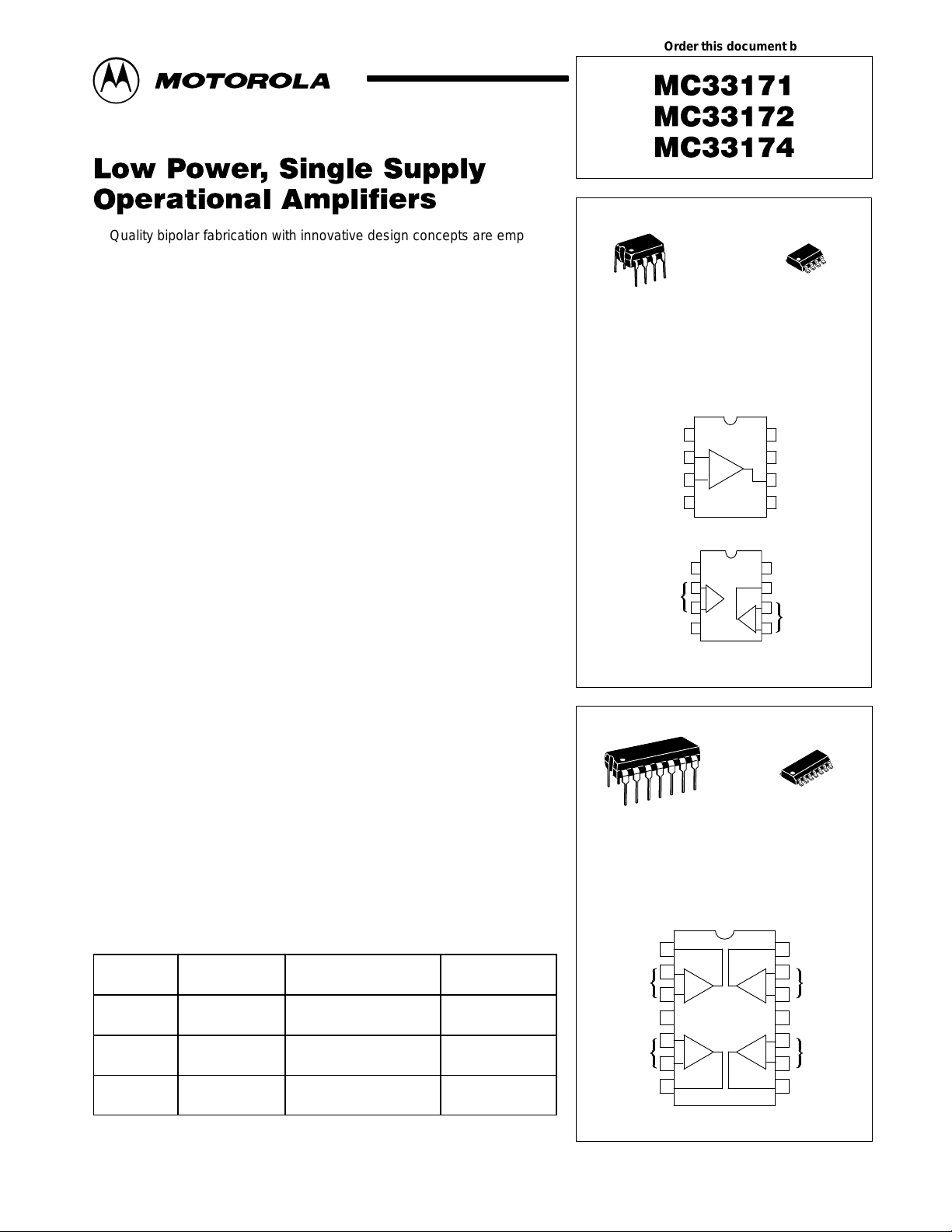
8
1
P SUFFIX
PLASTIC PACKAGE
CASE 626
PIN CONNECTIONS
Offset Null
Inv. Input
Noninv. Input
V
EE
Output 1 V
Inputs 1
V
EE
14
1
P SUFFIX
PLASTIC PACKAGE
CASE 646
DUAL
PLASTIC PACKAGE
1
2
–
+
3
4
(Single, Top View)
1
1
2
–
2
+
3
4
(Top View)
–
+
QUAD
PLASTIC PACKAGE
8
1
D SUFFIX
CASE 751
(SO–8)
8
NC
7
V
CC
Output
6
Offset Null
5
8
CC
7
Output 2
6
Inputs 2
5
14
1
D SUFFIX
CASE 751A
(SO–14)
ORDERING INFORMATION
Op Amp
Function
Single MC33171D
Dual MC33172D
Quad MC33174D
Device
MC33171P
MC33172P
MC33174P
Operating
Temperature Range
TA = –40° to +85°C
TA = –40° to +85°C
TA = –40° to +85°C
TA = –40° to +85°C
TA = –40° to +85°C
TA = –40° to +85°C
MOTOROLA ANALOG IC DEVICE DATA
Package
SO–8
Plastic DIP
SO–8
Plastic DIP
SO–14
Plastic DIP
PIN CONNECTIONS
Output 1
Inputs 1
Inputs 2
Output 2
Motorola, Inc. 1996 Rev 0
1
2
–
1
3
+
4
V
CC
5
+
23
–
6
78
(Top View)
14
Output 4
13
–
4
+
+
–
Inputs 4
12
11
V
EE
10
Inputs 3
9
Output 3
1
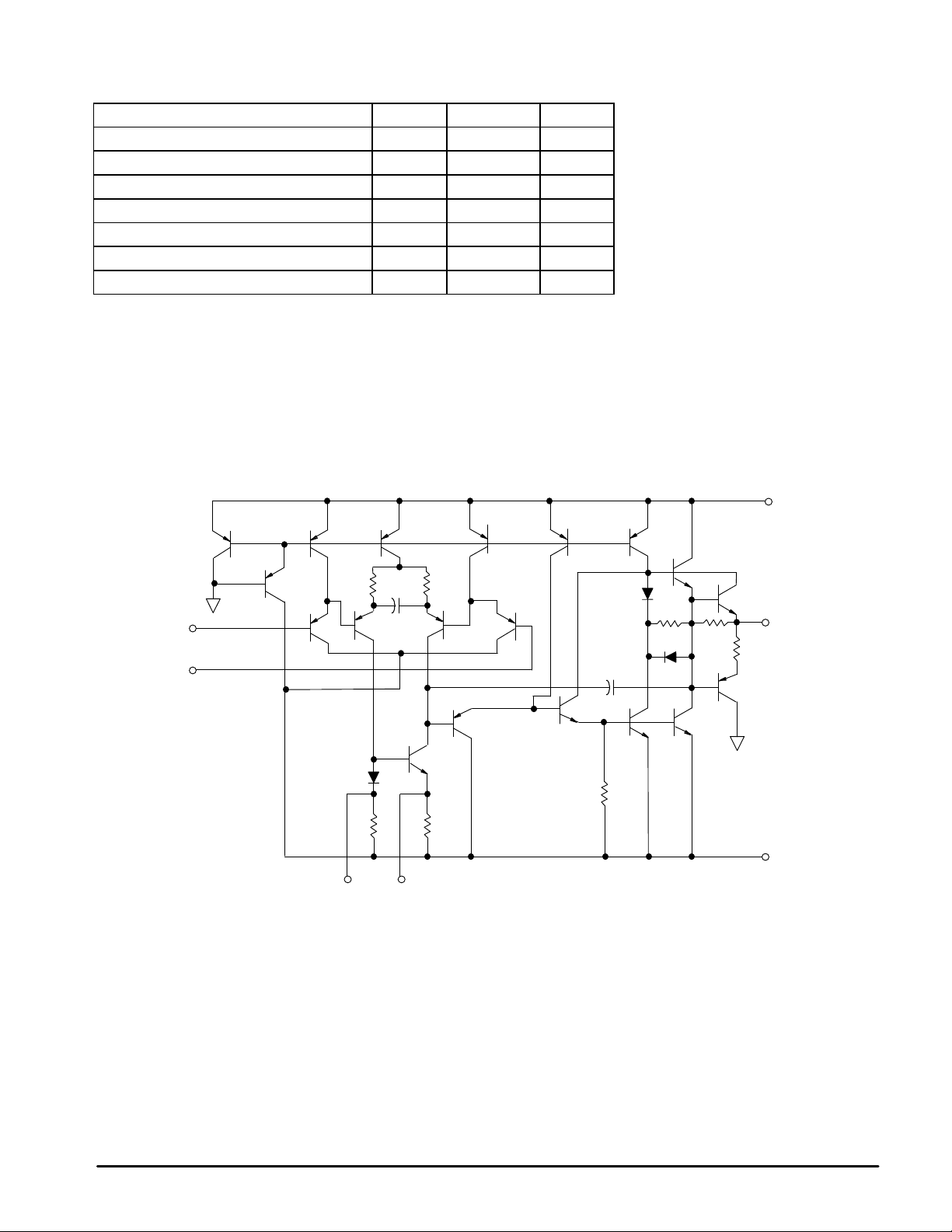
MC33171 MC33172 MC33174
MAXIMUM RATINGS
Rating Symbol Value Unit
Supply Voltage VCC/V
Input Differential Voltage Range V
Input Voltage Range V
Output Short Circuit Duration (Note 2) t
Operating Ambient Temperature Range T
Operating Junction Temperature T
Storage Temperature Range T
NOTES: 1. Either or both input voltages must not exceed the magnitude of VCC or V
2.Power dissipation must be considered to ensure maximum junction temperature (TJ)
is not exceeded.
EE
IDR
IR
SC
A
J
stg
Representative Schematic Diagram
(Each Amplifier)
±22 V
(Note 1) V
(Note 1) V
Indefinite sec
–40 to +85 °C
+150 °C
–65 to +150 °C
EE.
–
Inputs
+
Q1
Bias
Q3 Q4 Q5 Q6 Q7
Q2
Q8
R1
C1
Q9 Q10
Q12
D1
R3 R4
Offset Null
(MC33171)
R2
Q11
Q13
Q14
Q17
D2
R6 R7
C2 D3
Q16Q15
R5
Q18
R8
Q19
Current
Limit
VEE/Gnd
V
CC
Output
2
MOTOROLA ANALOG IC DEVICE DATA
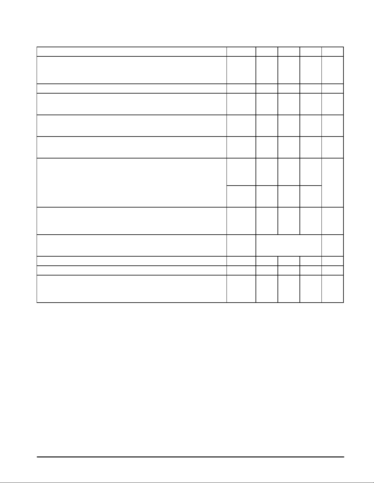
MC33171 MC33172 MC33174
DC ELECTRICAL CHARACTERISTICS (V
unless otherwise noted.)
Characteristics
Input Offset Voltage (VCM = 0 V)
VCC = +15 V, VEE = –15 V, TA = +25°C
VCC = +5.0 V, VEE = 0 V, TA = +25°C
VCC = +15 V, VEE = –15 V, TA = T
Average Temperature Coefficient of Offset Voltage ∆VIO/∆T — 10 — µV/°C
Input Bias Current (VCM = 0 V)
TA = +25°C
TA = T
Input Offset Current (VCM = 0 V)
TA = +25°C
TA = T
Large Signal Voltage Gain (VO = ±10 V< RL = 10 k)
TA = +25°C
TA = T
Output Voltage Swing
VCC = +5.0 V, VEE = 0 V, RL = 10 k, TA = +25°C
VCC = +15 V, VEE = –15 V, RL = 10 k, TA = +25°C
VCC = +15 V, VEE = –15 V, RL = 10 k, TA = T
VCC = +5.0 V, VEE = 0 V, RL = 10 k, TA = +25°C
VCC = +15 V, VEE = –15 V, RL = 10 k, TA = +25°C
VCC = +15 V, VEE = –15 V, RL = 10 k, TA = T
Output Short Circuit (TA = +25°C)
Input Overdrive = 1.0 V , Output to Ground
Input Common Mode Voltage Range
TA = +25°C
TA = T
Common Mode Rejection Ratio (RS ≤ 10 k) TA = +25°C CMRR 80 90 — dB
Power Supply Rejection Ratio (RS = 100 Ω) TA = +25°C PSRR 80 100 — dB
Power Supply Current (Per Amplifier)
VCC = +5.0 V, VEE = 0 V, TA = +25°C
VCC = +15 V, VEE = –15 V, TA = +25°C
VCC = +15 V, VEE = –15 V, TA = T
NOTE: 3. T
low
low
low
Source
Sink
low
low
to T
high
to T
high
to T
high
to T
high
= –40°CT
high
= +85°C
low
low
to T
to T
= +15 V, VEE = –15 V, RL connected to ground, TA = T
CC
Symbol Min Typ Max Unit
V
IO
high
I
IB
I
IO
A
VOL
V
OH
to T
low
high
V
OL
to T
low
high
I
SC
V
ICR
I
D
high
to T
low
high
—
—
—
—
—
—
—
50
25
3.5
13.6
13.3
—
—
—
3.0
15
—
—
—
2.0
2.5
—
20
—
5.0
—
500
—
4.3
14.2
—
0.05
–14.2
—
5.0
27
VEE to (VCC –1.8)
VEE to (VCC –2.2)
180
220
—
[Note 3],
mV
4.5
5.0
6.5
100
200
20
40
V/mV
—
—
—
—
—
0.15
–13.6
–13.3
mA
—
—
250
250
300
nA
nA
V
V
µA
MOTOROLA ANALOG IC DEVICE DATA
3
MC33171 MC33172 MC33174
AC ELECTRICAL CHARACTERISTICS (V
Characteristics Symbol Min Typ Max Unit
Slew Rate (Vin = –10 V to +10 V, RL = 10 k, CL = 100 pF)
AV +1
AV –1
Gain Bandwidth Product (f = 100 kHz) GBW 1.4 1.8 — MHz
Power Bandwidth
AV = +1.0 RL = 10 k, VO = 20 Vpp, THD = 5%
Phase Margin
RL = 10 k
RL = 10 k, CL = 100 pF
Gain Margin
RL = 10 k
RL = 10 k, CL = 100 pF
Equivalent Input Noise Voltage
RS = 100 Ω, f = 1.0 kHz
Equivalent Input Noise Current (f = 1.0 kHz) I
Differential Input Resistance
Vcm = 0 V
Input Capacitance C
Total Harmonic Distortion
AV = +10, RL = 10 k, 2.0 Vpp ≤ VO ≤ 20 Vpp, f = 10 kHz
Channel Separation (f = 10 kHz) CS — 120 — dB
Open Loop Output Impedance (f = 1.0 MHz) z
= +15 V, VEE = –15 V, RL connected to ground, TA = +25°C, unless otherwise noted.)
CC
SR
BWp — 35 — kHz
φ
m
A
m
e
n
n
R
in
i
THD — 0.03 — %
o
1.6
—
—
—
—
—
— 32 —
— 0.2 —
— 300 — MΩ
— 0.8 — pF
— 100 — Ω
2.1
2.1
60
45
15
5.0
—
—
—
—
—
—
V/µs
Degree
nV/ Hz√
pA/ Hz√
s
dB
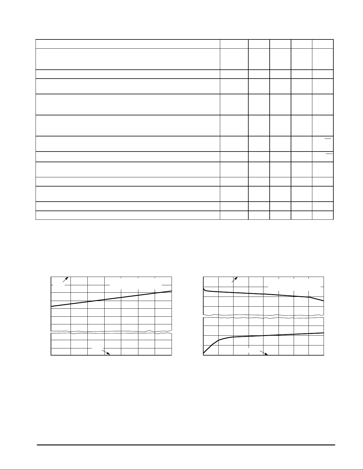
Figure 1. Input Common Mode V oltage Range
versus T emperature
0
V
CC
–0.8
–1.6
–2.4
0.1
V
0
–55 –25 0 25 50 75 100
ICR
V , INPUT COMMON MODE VOLTAGE RANGE (V)
TA, AMBIENT TEMPERATURE (°C)
VCC/VEE = ±1.5 V to ±22 V
∆
EE
VIO = 5.0 mV
Figure 2. Split Supply Output Saturation
versus Load Current
0
V
CC
–1.0
1.0
sat
V , OUTPUT SA TURATION VOLTAGE (V)
125 0 1.0 2.0 3.0 4.0
0
Source
Sink
V
IL, LOAD CURRENT (±mA)
VCC/VEE = ±5.0 V to ±22 V
EE
TA = 25
°
C
4
MOTOROLA ANALOG IC DEVICE DATA
 Loading...