

Device
Operating
Temperature Range
Package
SEMICONDUCTOR
TECHNICAL DATA
GaAs POWER AMPLIFIER
SUPPORT IC
ORDERING INFORMATION
MC33169DTB–4.0 TA = –40° to +85°C TSSOP–14
DTB SUFFIX
PLASTIC PACKAGE
CASE 948G
(TSSOP–14)
14
1
PIN CONNECTIONS
Order this document by MC33169/D
V
CC
Idle Mode Input
C2 Input
C1/C2
C1 Input
VO Output
VO Charge Pump
Capacitor+
Gnd
VO Charge Pump
Capacitor–
VBB Double
VBB Triple
Sense Input
Tx Power
Control Input
Gate Drive Output
(T op View)
1
2
3
4
5
6
7
14
13
12
11
10
9
8
1
MOTOROLA ANALOG IC DEVICE DATA
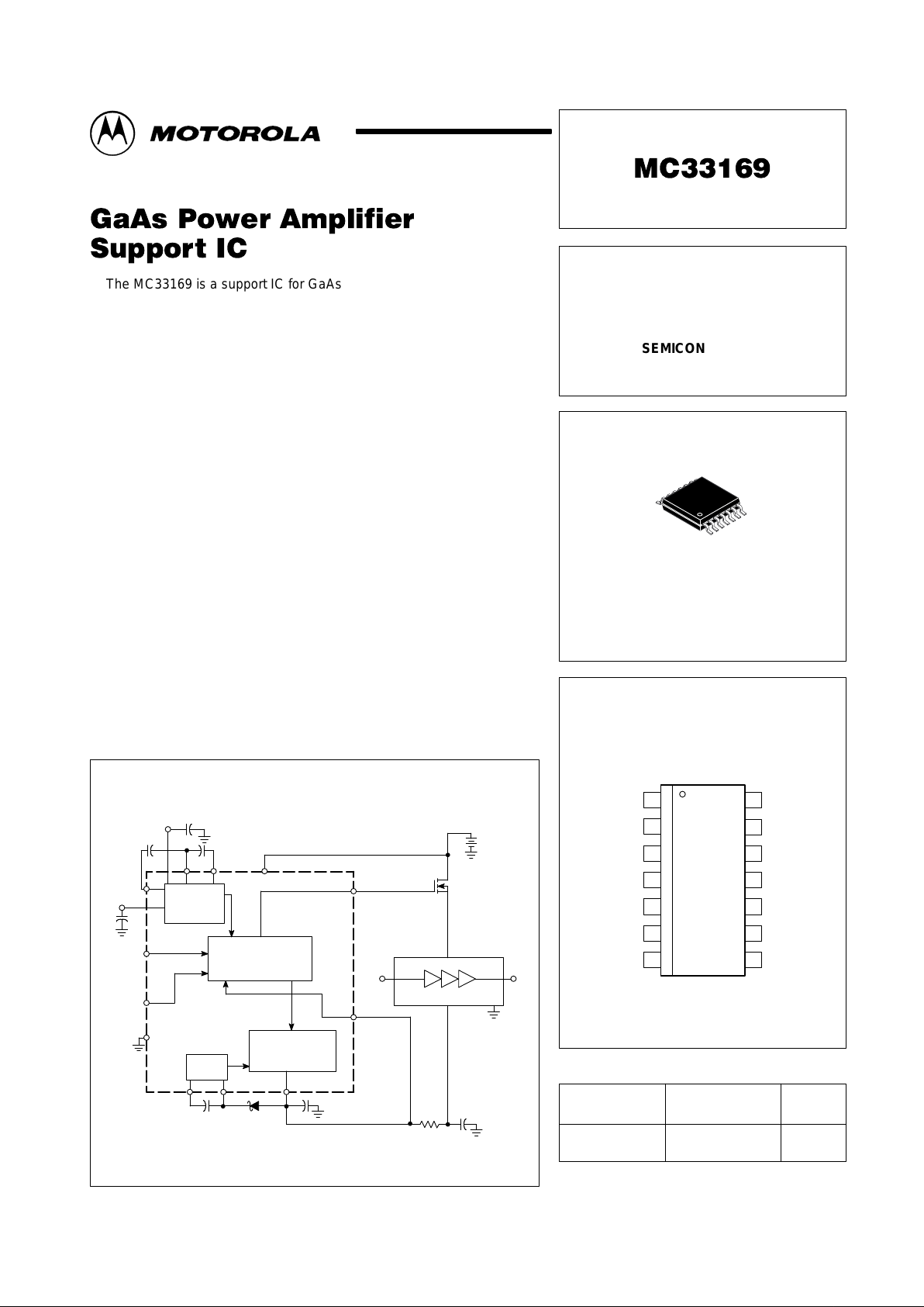
The MC33169 is a support IC for GaAs Power Amplifier Enhanced FETs
used in hand–held telephones such as GSM and PCS. This device provides
negative voltages for full depletion of Enhanced MESFETs as well as a
priority management system of drain switching, ensuring that the negative
voltage is always present before turning “on” the Power Amplifier. Additional
features include an idle mode input and a direct drive of the N–Channel drain
switch transistor. This product is available in a 4.0 V version intended for
control of the RF Power Amplifier in GSM, DCS1800 and PCS applications.
• Negative Regulated Output for Full Depletion of GaAs MESFETs
• Drain Switch Priority Management Circuit
• CMOS Compatible Inputs
• Idle Mode Input (Standby Mode) for Very Low Current Consumption
• Output Signal Directly Drives N–Channel FET
• Low Startup and Operating Current
Simplified Block Diagram
VBB Double
C3
V
CC
+–C1–+
C2
V
BB
Triple
C4
+
–
Tx Power
Control
Input
Idle
Mode Input
Gnd
C
p
+–
V
O
Output
(–4.0 V)
C
i
R
f
C
f
+–
+
RF
In
RF
Out
+
V
Battery
(2.7 to 7.0 V)
Gate Drive Output
Sense Input
V
BB
Generator
(Voltage Tripler)
Priority
Management
Negative
Generator
Charge
Pump
Power Amplifier
Sense
MC33169
MMSF4N01HD
21 14
8
10
457
6
13
9
3
11
+
12
This device contains 148 active transistors.
Motorola, Inc. 1998 Rev 2
MC33169
2
MOTOROLA ANALOG IC DEVICE DATA
MAXIMUM RATINGS
Rating Pin Symbol Value Unit
Power Supply Voltage 14 V
CC
9.5 V
Tx Power Control Input 9 VT
x
V
CC
V
Idle Mode Input 13 V
i
V
CC
V
Sense Input 10 V
Sense
–5.0 to 0 V
Negative Generator Output Source Current 4 I
SS
20 mA
Charge Pump Capacitor Current – I
max
60 mA
Diode Forward Current – I
Fmax
60 mA
Gate Drive Output Current 8 I
GO
5.0 mA
Power Dissipation and Thermal Characteristics –
Maximum Power Dissipation @ TA = 50°C P
D
417 mW
Thermal Resistance, Junction–to–Air R
θJA
240 °C/W
Operating Junction Temperature T
J
+150 °C
Operating Ambient Temperature – T
A
–40 to +85 °C
Storage Temperature Range – T
stg
–60 to +150 °C
NOTE: ESD data available upon request.
MC33169–4.0
ELECTRICAL CHARACTERISTICS (V
CC
= 4.8 V . For typical values TA = 25°C, for min/max values TA is the operating
ambient temperature range that applies, unless otherwise noted.)
Characteristic
Pin Symbol Min Typ Max Unit
VBB GENERATOR (VOLTAGE TRIPLER)
Oscillator Frequency – f
osc
90 100 110 kHz
Oscillator Duty Cycle – DC 35 50 65 %
Output Voltage (VCC = 3.0 V , IO = 3.0 mA) Double Voltage 12 V
BBD
4.6 5.0 – V
Output Voltage (VCC = 3.0 V , IO = 3.0 mA) Triple V oltage 11 V
BBT
6.1 7.0 –
Output Voltage (VCC = 7.2 V , IO = 3.0 mA) Triple Voltage 11 V
BBT
– 11.2 –
NEGATIVE GENERATOR OUTPUT
Output Voltage (IO = 3.0 mA) 4 V
O
–3.75 –4.0 –4.25 V
Output Voltage Ripple with Filter (Rf = 33 Ω, Cf = 4.7 µF) 4 V
r
mVpp
(IO = 0 to 5.0 mA) – 2.0 –
PRIORITY MANAGEMENT SECTION
Idle Mode Input 13
Input Voltage High State (Logic 1) V
IH
2.0 – VCC+0.2 V
Input Voltage Low State (Logic 0) V
IL
0 – 0.5 V
Input Current High State (Logic 1) I
IH
10 – 80 µA
Input Current Low State (Logic 0), i.e. Standby Mode I
IL
– – 1.0 µA
Tx Power Control Input 9
Input Voltage Range VT
x
0 – 3.1 V
Input Voltage “Of f” State (Zero RF Output Level) VT
x(off)
– 0.7 – V
Input Voltage “On” State (Maximum RF Output Level) VT
x(on)
– 2.7 – V
Input Resistance R
in
– 90 – kΩ
Bandwidth (–3.0 dB) B – 1.0 – MHz
Gate Drive Output 8
Voltage (VTx = 0 V) V
GO
– – 0.5 V
Voltage (VTx = 3.0 V) VCC+2.7 – –
Peak Current (Source and Sink) (VTx = 3.0 V) I
GO
– 3.0 – mA
Undervoltage Lockout Voltage on Sense Input (Magnitude) 10 V
sense
–3.0 –3.2 – V
TOTAL DEVICE POWER CONSUMPTION
ICC Operating (VTx = 3.0 V , IO = 3.0 mA) – I
CC
– 10 15 mA
ICC Operating (VTx = 0 V, IO = 3.0 mA) – I
CC
– 12 15 mA
ICC Operating (VTx = 0 V, IO = 0 mA) – 4.0 5.0
Standby Mode (Idle Mode Input = 0 V) – I
CC
– – 1.0 µA
MC33169
3
MOTOROLA ANALOG IC DEVICE DATA
MC33169–4.0
ELECTRICAL CHARACTERISTICS (V
CC
= 2.7 V . For typical values TA = 25°C, for min/max values TA is the operating
ambient temperature range that applies, unless otherwise noted.)
Characteristic
Pin Symbol Min Typ Max Unit
VBB GENERATOR (VOLTAGE TRIPLER)
Oscillator Frequency – f
osc
90 100 110 kHz
Oscillator Duty Cycle – DC 35 50 65 %
Output Voltage (VCC = 3.0 V , IO = 3.0 mA) V
Double Voltage 12 V
BBD
4.6 5.0 –
Triple V oltage 11 V
BBT
6.1 7.0 –
Triple V oltage (VCC = 7.2 V , IO = 3.0 mA) 11 V
BBT
– 11.2 –
NEGATIVE GENERATOR OUTPUT
Output Voltage (IO = 1.0 mA) 4 V
O
–3.75 –4.0 –4.25 V
Output Voltage Ripple with Filter (Rf = 33 Ω, Cf = 4.7 µF) 4 V
r
mVpp
(IO = 0 to 5.0 mA) – 2.0 –
PRIORITY MANAGEMENT SECTION
Idle Mode Input 13
Input Voltage High State (Logic 1) V
IH
2.0 – VCC+0.2 V
Input Voltage Low State (Logic 0) V
IL
0 – 0.5 V
Input Current High State (Logic 1) I
IH
10 – 80 µA
Input Current Low State (Logic 0), i.e. Standby Mode I
IL
– – 1.0 µA
Tx Power Control Input 9
Input Voltage Range VT
x
0 – 3.0 V
Input Voltage “Of f” State (Zero RF Output Level) VT
x(off)
– 0.7 – V
Input Voltage “On” State (Maximum RF Output Level) VT
x(on)
– 2.7 – V
Input Resistance R
in
– 90 – kΩ
Bandwidth (–3.0 dB) B – 1.0 – MHz
Gate Drive Output 8
Voltage (VTx = 0 V) V
GO
– – 0.5 V
Voltage (VTx = 3.0 V) VCC+2.7 – –
Peak Current (Source and Sink) (VTx = 3.0 V) I
GO
– 3.0 – mA
Undervoltage Lockout Voltage on Sense Input (Magnitude) 10 V
sense
–3.0 –3.2 – V
TOTAL DEVICE POWER CONSUMPTION
ICC Operating (VTx = 3.0 V) 14 I
CC
mA
(IO = 3.0 mA) – – 15
(IO = 1.0 mA) – – 9.0
ICC Operating (VTx = 0 V) 14 I
CC
mA
(IO = 3.0 mA) – – 13
(IO = 1.0 mA) – – 9.0
(IO = 0 mA) – 4.5 6.0
Standby Mode (Idle Mode Input = 0 V) 14 I
CC
– – 1.0 µA
PRIORITY MANAGEMENT TRUTH TABLE
Control Inputs Outputs
Idle Mode Tx Power Control V
O
Gate Drive
0
1
0
1
0
0
1
1
Off
–4.0 V
Off
–4.0 V
0.5 V max
0.5 V max
0.5 V max
VCC + 2.7 V min
 Loading...