

Motorola MC33153D, MC33153DR2, MC33153P Datasheet
The MC33153 is specifically designed as an IGBT driver for high power
applications that include ac induction motor control, brushless dc motor
control and uninterruptable power supplies. Although designed for driving
discrete and module IGBTs, this device offers a cost effective solution for
driving power MOSFETs and Bipolar Transistors. Device protection features
include the choice of desaturation or overcurrent sensing and undervoltage
detection. These devices are available in dual–in–line and surface mount
packages and include the following features:
• High Current Output Stage: 1.0 A Source/2.0 A Sink
• Protection Circuits for Both Conventional and Sense IGBTs
• Programmable Fault Blanking Time
• Protection against Overcurrent and Short Circuit
• Undervoltage Lockout Optimized for IGBT’s
• Negative Gate Drive Capability
• Cost Effectively Drives Power MOSFETs and Bipolar Transistors
Order this document by MC33153/D
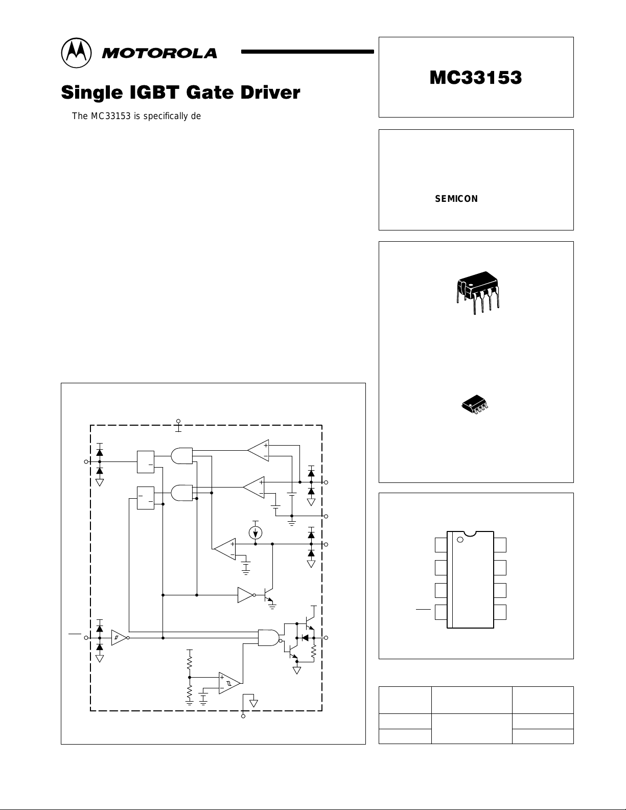
SINGLE IGBT
GATE DRIVER
SEMICONDUCTOR
TECHNICAL DATA
8
1
Representative Block Diagram
V
CC
6
V
CC
Short Circuit
V
V
V
EE
CC
EE
Latch
Q
Overcurrent
Latch
Q
Fault
Output
7
Input
4 5
V
CC
S
R
S
R
V
CC
This device contains 133 active transistors.
Short Circuit
Comparator
Overcurrent
Comparator
Fault Blanking/
Desaturation
Comparator
Under
Voltage
Lockout
12 V/
11 V
3
65 mV
V
CC
6.5 V
V
EE
130 mV
270
µ
A
Output
Stage
100 k
V
EE
V
CC
V
EE
V
CC
V
EE
V
CC
Current
Sense
1
Input
Kelvin
Gnd
2
Fault
Blanking/
8
Desaturation
Input
Drive
Output
Current Sense
Input
Kelvin Gnd
V
EE
Input
ORDERING INFORMATION
Device
MC33153D
MC33153P
P SUFFIX
PLASTIC PACKAGE
CASE 626
8
1
D SUFFIX
PLASTIC PACKAGE
CASE 751
(SO–8)
PIN CONNECTIONS
18
2
3
4
(Top View)
Operating
Temperature Range
TA = –40° to +105°C
Fault Blanking/
Desaturation Input
7
Fault Output
6
V
CC
5
Drive Output
Package
SO–8
DIP–8
MOTOROLA ANALOG IC DEVICE DATA
Motorola, Inc. 1998 Rev 2
1
MC33153
MAXIMUM RATINGS
Rating Symbol Value Unit
Power Supply Voltage V
VCC to V
Kelvin Ground to VEE (Note 1) KGnd – V
Logic Input V
Current Sense Input V
Blanking/Desaturation Input V
Gate Drive Output
Source Current
Sink Current
Diode Clamp Current
Fault Output
Source Current
Sink Curent
Power Dissipation and Thermal Characteristics
D Suffix SO–8 Package, Case 751
Maximum Power Dissipation @ TA = 50°C
Thermal Resistance, Junction–to–Air
P Suffix DIP–8 Package, Case 626
Maximum Power Dissipation @ TA = 50°C
Thermal Resistance, Junction–to–Air
Operating Junction Temperature T
Operating Ambient Temperature T
Storage Temperature Range T
NOTE: ESD data available upon request.
EE
VCC – V
in
S
BD
I
O
I
FO
P
D
R
θJA
P
D
R
θJA
J
A
stg
EE
EE
20
20
VEE –0.3 to V
–0.3 to V
–0.3 to V
–40 to +105 °C
–65 to +150 °C
CC
CC
CC
1.0
2.0
1.0
25
10
0.56
180
1.0
100
+150 °C
V
V
V
A
mA
W
°C/W
W
°C/W
ELECTRICAL CHARACTERISTICS (V
TA = 25°C, for min/max values TA is the operating ambient temperature range that applies (Note 2), unless otherwise noted.)
Characteristic
LOGIC INPUT
Input Threshold Voltage
High State (Logic 1)
Low State (Logic 0)
Input Current
High State (VIH = 3.0 V)
Low State (VIL = 1.2 V)
DRIVE OUTPUT
Output Voltage
Low State (I
High State (I
Output Pull–Down Resistor R
FAULT OUTPUT
Output voltage
Low State (I
High State (I
SWITCHING CHARACTERISTICS
Propagation Delay (50% Input to 50% Output CL = 1.0 nF)
Logic Input to Drive Output Rise
Logic Input to Drive Output Fall
Drive Output Rise Time (10% to 90%) CL = 1.0 nF t
Drive Output Fall Time (90% to 10%) CL = 1.0 nF t
NOTES: 1. Kelvin Ground must always be between VEE and VCC.
2.Low duty cycle pulse techniques are used during test to maintain the junction temperature as close to ambient as possible.
= 1.0 A)
Sink
= 500 mA)
Source
= 5.0 mA)
Sink
= 20 mA)
Source
T
= –40°C for MC33153 T
low
= 15 V, VEE = 0 V, Kelvin Gnd connected to VEE. For typical values
CC
Symbol Min Typ Max Unit
= +105°C for MC33153
high
V
IH
V
IL
I
IH
I
IL
V
OL
V
OH
PD
V
FL
V
FH
t
PLH(in/out)
t
PHL (in/out)
r
f
–
1.2
–
–
–
12
– 100 200 kΩ
–
12
–
–
– 17 55 ns
– 17 55 ns
2.70
2.30
130
50
2.0
13.9
0.2
13.3
80
120
3.2
500
100
2.5
1.0
300
300
V
–
µA
V
–
V
–
ns
2
MOTOROLA ANALOG IC DEVICE DATA
MC33153
ELECTRICAL CHARACTERISTICS (continued) (V
TA = 25°C, for min/max values TA is the operating ambient temperature range that applies (Note 2), unless otherwise noted.)
Characteristic UnitMaxTypMinSymbol
SWITCHING CHARACTERISTICS (continued)
Propagation Delay µs
Current Sense Input to Drive Output t
Fault Blanking/Desaturation Input to Drive Output t
UVLO
Startup Voltage VCC
Disable Voltage VCC
COMPARATORS
Overcurrent Threshold Voltage (V
Short Circuit Threshold Voltage (V
Fault Blanking/Desaturation Threshold (V
Current Sense Input Current (VSI = 0 V) I
FAULT BLANKING/DESATURATION INPUT
Current Source (V
Discharge Current (V
TOTAL DEVICE
Power Supply Current
Standby (V
Operating (CL = 1.0 nF, f = 20 kHz)
NOTES: 1. Kelvin Ground must always be between VEE and VCC.
Pin 4
2.Low duty cycle pulse techniques are used during test to maintain the junction temperature as close to ambient as possible.
T
= –40°C for MC33153 T
low
= 0 V, V
Pin8
= 15 V, V
Pin8
= VCC, Output Open)
> 7.0 V) V
Pin8
> 7.0 V) V
Pin8
> 100 mV) V
Pin1
= 0 V) I
Pin4
= 5.0 V) I
Pin4
= +105°C for MC33153
high
= 15 V, VEE = 0 V, Kelvin Gnd connected to VEE. For typical values
CC
P(OC)
P(FLT)
start
dis
SOC
SSC
th(FLT)
SI
chg
dschg
I
CC
– 0.3 1.0
– 0.3 1.0
11.3 12 12.6 V
10.4 11 1 1.7 V
50 65 80 mV
100 130 160 mV
6.0 6.5 7.0 V
– –1.4 –10 µA
–200 –270 –300 µA
1.0 2.5 – mA
–
–
7.2
7.9
14
20
mA
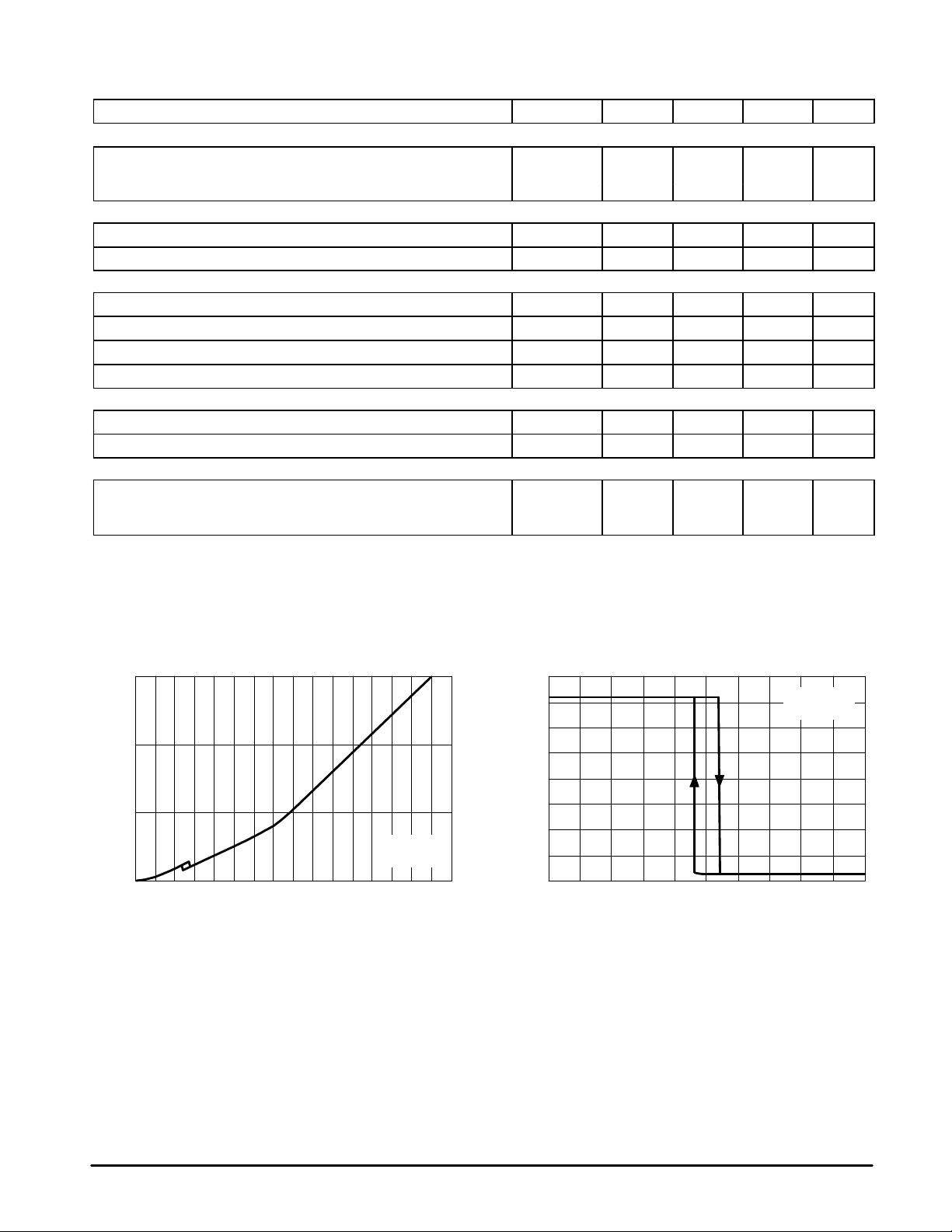
Figure 1. Input Current versus Input Voltage
1.5
1.0
0.5
, INPUT CURRENT (mA)
in
I
0
2.0 4.0 6.0 8.0 10 12 14 16
0
Vin, INPUT VOLTAGE (V)
VCC = 15 V
°
C
TA = 25
Figure 2. Output V oltage versus Input Voltage
16
14
12
10
8.0
6.0
, OUTPUT VOL TAGE (V)
4.0
O
V
2.0
0
0
1.0 2.0 3.0 4.0
Vin, INPUT VOLTAGE (V)
VCC = 15 V
°
C
TA = 25
5.0
MOTOROLA ANALOG IC DEVICE DATA
3
MC33153
, INPUT THRESHOLD VOLTAGE (V)V
IL
– V
IH
Figure 3. Input Threshold V oltage
versus T emperature
3.2
3.0
2.8
2.6
2.4
2.2
2.0
–40 –20 0 20 40 60 80 100 120 140
–60
V
IH
V
IL
TA, AMBIENT TEMPERATURE (°C)
VCC = 15 V
Figure 5. Drive Output Low State Voltage
versus T emperature
2.5
2.0
1.5
I
= 1.0 A
Sink
= 500 mA
, INPUT THRESHOLD VOLTAGE (V)V
IL
– V
IH
Figure 4. Input Threshold V oltage
versus Supply V oltage
2.8
V
2.7
2.6
2.5
2.4
2.3
2.2
13 14 15 16 17 18 19 20
12
IH
V
IL
VCC, SUPPLY VOLTAGE (V)
Figure 6. Drive Output Low State Voltage
versus Sink Current
2.0
1.6
1.2
TA = 25°C
1.0
0.5
, OUTPUT LOW STATE VOLTAGE (V)
OL
V
0
–60
14.0
13.9
13.8
13.7
13.6
, DRIVE OUTPUT HIGH STATE VOLTAGE (V)
13.5
OH
–60
V
= 250 mA
VCC = 15 V
–40 –20 0 20 40 60 80 100 120 140
TA, AMBIENT TEMPERATURE (°C)
Figure 7. Drive Output High State Voltage
versus T emperature
VCC = 15 V
I
= 500 mA
Source
–40 –20 0 20 40 60 80 100 120 140
°
TA, AMBIENT TEMPERATURE (
C)
0.8
0.4
, OUTPUT LOW STATE VOLTAGE (V)
OL
V
0
0
15.0
14.6
14.2
13.8
13.4
, DRIVE OUTPUT HIGH STATE VOLTAGE (V)
13.0
OH
0
V
TA = 25°C
VCC = 15 V
0.2 0.4 0.6 0.8 1.0
I
, OUTPUT SINK CURRENT (A)
Sink
Figure 8. Drive Output High State Voltage
versus Source Current
VCC = 15 V
°
C
TA = 25
0.1 0.2 0.3 0.4 0.5
I
, OUTPUT SOURCE CURRENT (A)
Source
4
MOTOROLA ANALOG IC DEVICE DATA
 Loading...