

MOTOROLA MC34151D, MC34151DR2, MC34151P, MC33151D, MC33151DR2 Datasheet
...
MC34151, MC33151
High Speed Dual
MOSFET Drivers
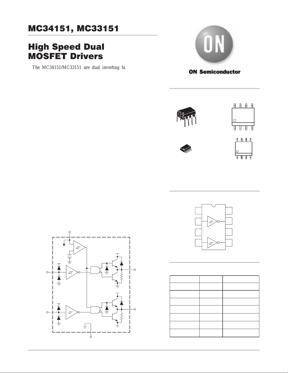
The MC34151/MC33151 are dual inverting high speed drivers
specifically designed for applications that require low current digital
circuitry to drive large capacitive loads with high slew rates. These
devices feature low input current making them CMOS and LSTTL
logic compatible, input hysteresis for fast output switching that is
independent of input transition time, and two high current totem pole
outputs ideally suited for driving power MOSFETs. Also included is
an undervoltage lockout with hysteresis to prevent erratic system
operation at low supply voltages.
Typical applications include switching power supplies, dc to dc
converters, capacitor charge pump voltage doublers/inverters, and
motor controllers.
These devices are available in dual–in–line and surface mount
packages.
• T wo Independent Channels with 1.5 A Totem Pole Output
• Output Rise and Fall Times of 15 ns with 1000 pF Load
• CMOS/LSTTL Compatible Inputs with Hysteresis
• Undervoltage Lockout with Hysteresis
• Low Standby Current
• Efficient High Frequency Operation
• Enhanced System Performance with Common Switching Regulator
Control ICs
• Pin Out Equivalent to DS0026 and MMH0026
http://onsemi.com
MARKING
DIAGRAMS
8
PDIP–8
P SUFFIX
8
1
8
1
x = 3 or 4
A = Assembly Location
WL, L = Wafer Lot
YY, Y = Year
WW, W= Work Week
CASE 626
SO–8
D SUFFIX
CASE 751
MC3x151P
AWL
YYWW
1
8
3x151
ALYW
1
PIN CONNECTIONS
Logic Input A
Logic Input B
Representative Block Diagram
V
CC
6
+
+
–
+
+
2
+
4
5.7V
Gnd
3
1
Logic Input A
Logic Input B
+
Drive Output A
7
100k
+
Drive Output B
5
100k
Device Package Shipping
MC34151D SO–8 98 Units/Rail
MC34151DR2 SO–8 2500 Tape & Reel
MC34151P PDIP–8
MC33151D SO–8
MC33151DR2 SO–8 2500 Tape & Reel
MC33151P PDIP–8 50 Units/Rail
MC33151VDR2 SO–8 2500 Units/Rail
2
3
Gnd
45
(Top View)
ORDERING INFORMATION
8N.C.
N.C.
7
Drive Output A
6
V
CC
Drive Output B
50 Units/Rail
98 Units/Rail
Semiconductor Components Industries, LLC, 2000
April, 2000 – Rev. 1
1 Publication Order Number:
MC34151/D
MC34151, MC33151
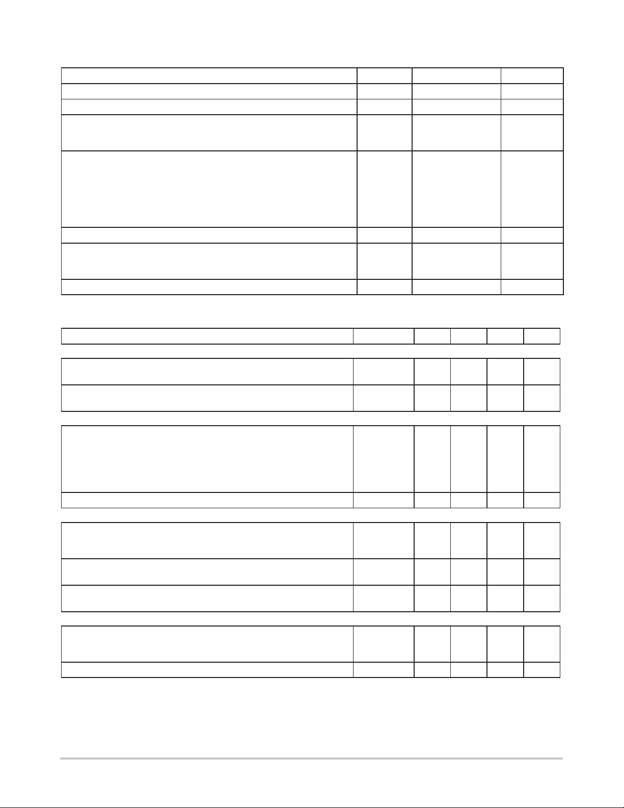
MAXIMUM RATINGS
Rating Symbol Value Unit
Power Supply Voltage V
Logic Inputs (Note 1.) V
Drive Outputs (Note 2.)
Totem Pole Sink or Source Current
Diode Clamp Current (Drive Output to VCC)
Power Dissipation and Thermal Characteristics
D Suffix SO–8 Package Case 751
Maximum Power Dissipation @ TA = 50°C
Thermal Resistance, Junction–to–Air
P Suffix 8–Pin Package Case 626
Maximum Power Dissipation @ TA = 50°C
Thermal Resistance, Junction–to–Air
Operating Junction Temperature T
Operating Ambient Temperature
MC34151
MC33151
Storage Temperature Range T
I
CC
in
I
O
O(clamp)
P
D
R
θJA
P
D
R
θJA
J
T
A
stg
20 V
–0.3 to V
–65 to +150 °C
CC
1.5
1.0
0.56
180
1.0
100
+150 °C
0 to +70
–40 to +85
°C/W
°C/W
°C
V
A
W
W
ELECTRICAL CHARACTERISTICS (V
Characteristics
LOGIC INPUTS
Input Threshold Voltage – High State Logic 1
Input Threshold Voltage – Low State Logic 0
Input Current – High State (VIH = 2.6 V)
Input Current – Low State (VIL = 0.8 V)
DRIVE OUTPUT
Output Voltage – Low State (I
Output Voltage – Low State (I
Output Voltage – Low State (I
Output Voltage – High State (I
Output Voltage – High State (I
Output Voltage – High State (I
Output Pull–Down Resistor R
SWITCHING CHARACTERISTICS (TA = 25°C)
Propagation Delay (10% Input to 10% Output, CL = 1.0 nF)
Logic Input to Drive Output Rise
Logic Input to Drive Output Fall
Drive Output Rise Time (10% to 90%) CL = 1.0 nF
Drive Output Rise Time (10% to 90%) CL = 2.5 nF
Drive Output Fall Time (90% to 10%) CL = 1.0 nF
Drive Output Fall Time (90% to 10%) CL = 2.5 nF
TOTAL DEVICE
Power Supply Current
Standby (Logic Inputs Grounded)
Operating (CL = 1.0 nF Drive Outputs 1 and 2, f = 100 kHz)
Operating Voltage V
1. For optimum switching speed, the maximum input voltage should be limited to 10 V or VCC, whichever is less.
2. Maximum package power dissipation limits must be observed.
3. T
=0°C for MC34151 T
low
–40°C for MC33151 +85°C for MC33151
= 10 mA)
Sink
= 50 mA)
Sink
= 400 mA)
Sink
Source
Source
Source
= 10 mA)
= 50 mA)
= 400 mA)
= 12 V, for typical values TA = 25°C, for min/max values TA is the only operating
CC
ambient temperature range that applies [Note 3.], unless otherwise noted.)
Symbol Min Typ Max Unit
= +70°C for MC34151
high
V
IH
V
IL
I
IH
I
IL
V
OL
V
OH
PD
t
PLH(in/out)
t
PHL(in/out)
t
r
t
f
I
CC
CC
2.6
–
–
–
–
–
–
10.5
10.4
9.5
– 100 – kΩ
–
–
–
–
–
–
–
–
6.5 – 18 V
1.75
1.58
200
20
0.8
1.1
1.7
11.2
11.1
10.9
35
36
14
31
16
32
6.0
10.5
–
0.8
500
100
1.2
1.5
2.5
–
–
–
100
100
30
–
30
–
10
15
V
µA
V
ns
ns
ns
mA
http://onsemi.com
2
12
V
4.7 0.1
+
6
MC34151, MC33151
Logic Input
2.4
2.0
1.6
1.2
+
2
50 C
+
4
+
+
–
+
5.7V
3
+
Drive Output
7
100k
+
5
100k
L
Logic Input
tr, tf ≤ 10 ns
Drive Output
5.0 V
0 V
10%
t
PHL
t
f
90%
90%
t
PLH
10%
t
Figure 1. Switching Characteristics T est Circuit Figure 2. Switching Waveform Definitions
2.2
VCC = 12 V
TA = 25°C
2.0
1.8
1.6
Upper Threshold
Low State Output
VCC = 12 V
r
0.8
, INPUT CURRENT (mA)
in
I
0.4
0
0 2.0 4.0 6.0 8.0 10 12 –55 –25 0 25 50 75 100 125
Vin, INPUT VOLTAGE (V)
Figure 3. Logic Input Current versus
Input Voltage
200
VCC = 12 V
CL = 1.0 nF
160
TA = 25°C
120
80
40
, DRIVE OUTPUT PROPAGATION DELA Y (ns)
0
–1.6 –1.2 –0.8 –0.4 0 0 1.0 2.0 3.0 4.0
Vin, INPUT OVERDRIVE VOLTAGE BELOW LOWER THRESHOLD (V)
PLH(IN/OUT)
t
Overdrive Voltage is with Respect
to the Logic Input Lower Threshold
V
th(lower)
Figure 5. Drive Output Low–to–High Propagation
Delay versus Logic Overdrive V oltage
1.4
, INPUT THRESHOLD VOLTAGE (V)
1.2
th
V
1.0
Lower Threshold
High State Output
TA, AMBIENT TEMPERATURE (°C)
Figure 4. Logic Input Threshold V oltage
versus T emperature
200
160
120
80
40
, DRIVE OUTPUT PROPAGATION DELA Y (ns)
0
Vin, INPUT OVERDRIVE VOLTAGE ABOVE UPPER THRESHOLD (V)
PHL(IN/OUT)
t
Overdrive Voltage is with Respect
to the Logic Input Lower Threshold
V
th(upper)
VCC = 12 V
CL = 1.0 nF
TA = 25°C
Figure 6. Drive Output High–to–Low Propagation
Delay versus Logic Input Overdrive V oltage
http://onsemi.com
3
MC34151, MC33151
V
,
T
T
T
T
N
V
LT
G
(V)
90%
10%
Logic Input
Drive Output
50 ns/DIV
VCC = 12 V
Vin = 5 V to 0 V
CL = 1.0 nF
TA = 25°C
Figure 7. Propagation Delay Figure 8. Drive Output Clamp Voltage
0
E
A
–1.0
O
–2.0
IO
–3.0
URA
3.0
SA
PU
2.0
OU
1.0
sat
0
0 0.2 0.4 0.6 0.8 1.0 1.2 1.4
IO, OUTPUT LOAD CURRENT (A)
V
CC
Sink Saturation
(Load to VCC)
Source Saturation
(Load to Ground)
VCC = 12 V
80 µs Pulsed Load
120 Hz Rate
TA = 25°C
Gnd
Figure 9. Drive Output Saturation Voltage
versus Load Current
90%
3.0
2.0
1.0
0
, OUTPUT CLAMP VOLTAGE (V)
0
clamp
V
–1.0
High State Clamp
(Drive Output Driven Above VCC)
V
CC
Gnd
0 0.2 0.4 0.6 0.8 1.0 1.2 1.4
IO, OUTPUT LOAD CURRENT (A)
(Drive Output Driven Below Ground)
VCC = 12 V
80 µs Pulsed Load
120 Hz Rate
TA = 25°C
Low State Clamp
versus Clamp Current
0
Source Saturation
–0.5
(Load to Ground)
–0.7
–0.9
–1.1
1.9
1.7
1.5
1.0
, OUTPUT SATURATION VOLTAGE(V)
0.8
sat
V
Sink Saturation
0.6
(Load to VCC)
0
–55 –25 0 25 50 75 100 125
V
CC
TA, AMBIENT TEMPERATURE (°C)
I
sink
I
sink
Gnd
I
source
I
source
= 400 mA
= 10 mA
= 10 mA
= 400 mA
VCC = 12 V
Figure 10. Drive Output Saturation Voltage
versus T emperature
90%
VCC = 12 V
Vin = 5 V to 0 V
CL = 1.0 nF
TA = 25°C
10%
VCC = 12 V
Vin = 5 V to 0 V
CL = 1.0 nF
TA = 25°C
10 ns/DIV
10%
10 ns/DIV
Figure 11. Drive Output Rise Time Figure 12. Drive Output Fall Time
http://onsemi.com
4
 Loading...