Motorola MC33143DW Datasheet

Order this document by MC33143/D
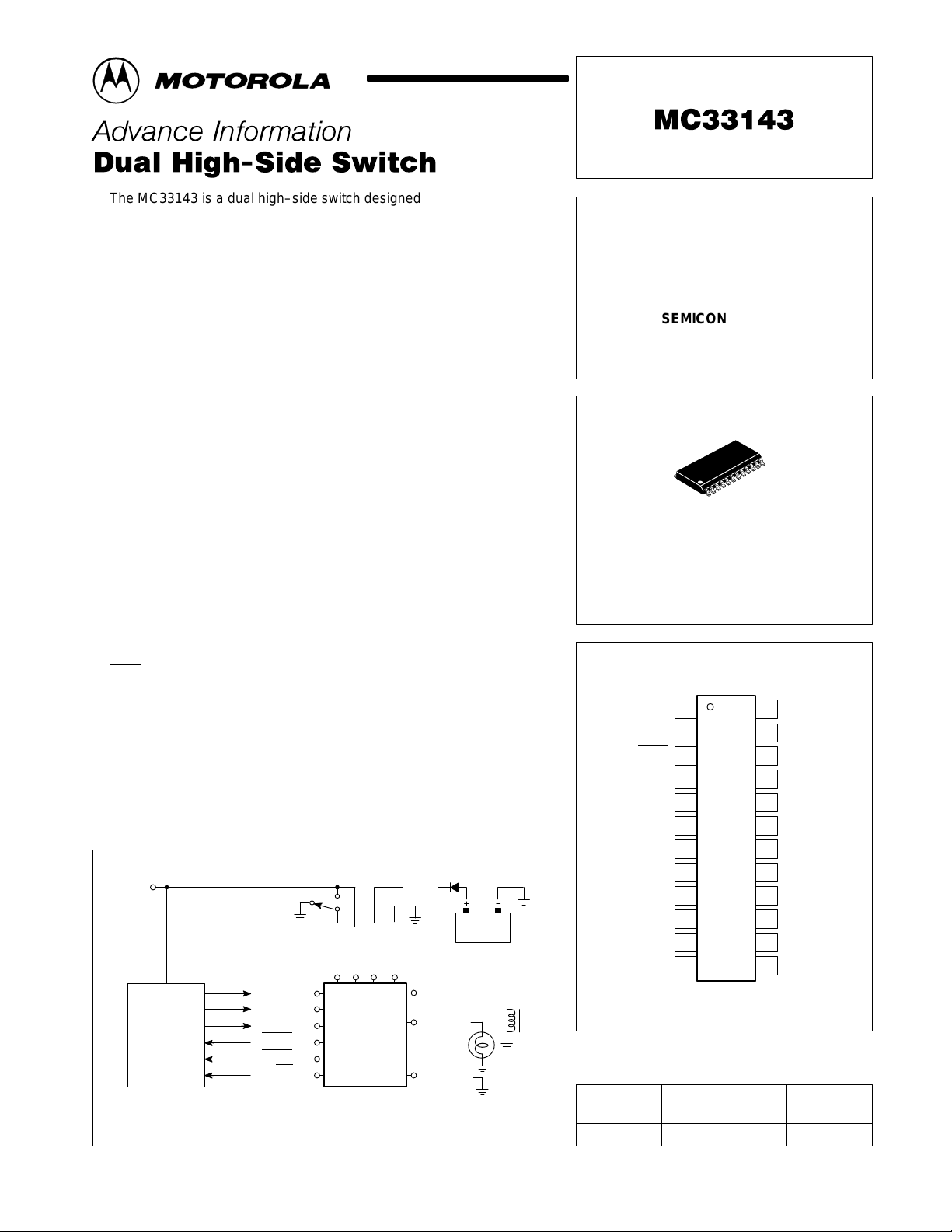
The MC33143 is a dual high–side switch designed for solenoid control in
harsh automotive applications, but is well suited for other environments. The
device can also be used to control small motors and relays as well as
solenoids. The MC33143 incorporates SMARTMOS technology, with
CMOS logic, bipolar/MOS analog circuitry, and DMOS power outputs. An
internal charge pump is incorporated for efficient gate enhancement of the
internal high–side power output devices. The outputs are designed to
provide current to low impedance solenoids. The MC33143 provides
individual output fault status reporting along with internal Overcurrent and
Over Temperature protection. The device also has Overvoltage protection,
with automatic recovery, which “globally” disables both outputs for the
duration of an Overvoltage condition. Each output has individual Overcurrent
and Over Temperature shutdown with automatic retry recovery. Outputs are
enabled with a CMOS logic high signal applied to an input to providing true
logic control. The outputs, when turned on, provide full supply (battery)
voltage across the solenoid coil.
The MC33143 is packaged in an economical 24 pin surface mount power
package and specified over an operating voltage of 5.5 V ≤ V
–40°C ≤ TA ≤ 125°C.
• Designed to Operate Over Wide Supply Voltages of 5.5 V to 26 V
• Dual High–Side Outputs Clamped to –10 V for Driving Inductive Loads
• Internal Charge Pump for Enhanced Gate Drive
• Interfaces Directly to a Microcontroller with Parallel Input Control
• Outputs Current Limited to 3.0 A to 6.0 A for Driving Incandescent Loads
• Chip Enable “Sleep Mode” for Power Conservation
• Individual Output Status Reporting
• Fault Interrupt Output for System Interrupt Use
• Output ON or OFF Open Load Detection
• Overvoltage Detection and Shutdown
• Output Over Temperature Detection and Shutdown with Automatic Retry
• Sustained Current Limit or Immediate Overcurrent Shutdown Output Modes
• Output Short to Ground Detection and Shutdown with Automatic Retry
• Output Short to V
SMARTMOS is a trademark of Motorola, Inc.
V
DD
V
P0
DD
P1
P2
MCU
P3
P4
IRQ
NOTE: Pins 5, 6, 7, 8, 17, 18, 19 and 20 provide electrical ground and heatsinking.
This document contains information on a new product. Specifications and information herein
are subject to change without notice.
MOTOROLA ANALOG IC DEVICE DATA
Detection
Pwr
Simplified Application
+V
Pwr
(16)
(11)
Pwr
DD
SFPD (14)
CEN (2)
IN1 (1)
IN2 (12)
STAT1
(13)
STAT2 (10)
INT (23)
This device contains 889 active transistors.
MC33143
GTST (15)
V
V
OUT1 (24)
OUT2 (13)
Gnd (Note)
< 26 V for
Pwr
Battery
DUAL HIGH–SIDE
SWITCH
SEMICONDUCTOR
TECHNICAL DATA
24
1
DW SUFFIX
PLASTIC PACKAGE
CASE 751E
(SOP (16+4+4)L)
PIN CONNECTIONS
23
22
21
20
19
18
17
16
15
14
13
OUT1
INT
N/C
V
Pwr
Gnd
Gnd
Gnd
Gnd
V
Pwr
GTST
SFPD
OUT2
Package
SOP–24L
1
124
IN1
CEN
2
STAT1
3
4
V
Pwr
Gnd
5
Gnd
6
Gnd
7
Gnd
8
9
V
Pwr
10
STAT2
V
11
DD
IN2
12
(Top View)
ORDERING INFORMATION
Operating
Device
MC33143DW TA = – 40° to +125°C
Motorola, Inc. 1996 Rev 0
Temperature Range

V
(9, 16)
Pwr
SFPD (14)
IN1 (1)
VDD (11)
GTST (15)
CEN (2)
IN2 (12)
Gnd (5) (See Note)
NOTE: Pins 5, 6, 7, 8, 17, 18, 19 and 20 should all be grounded so as to provide electrical as well as thermal heatsinking of the device.
Overvoltage
Shutdown
Bias
Charge
Pump
MC33143
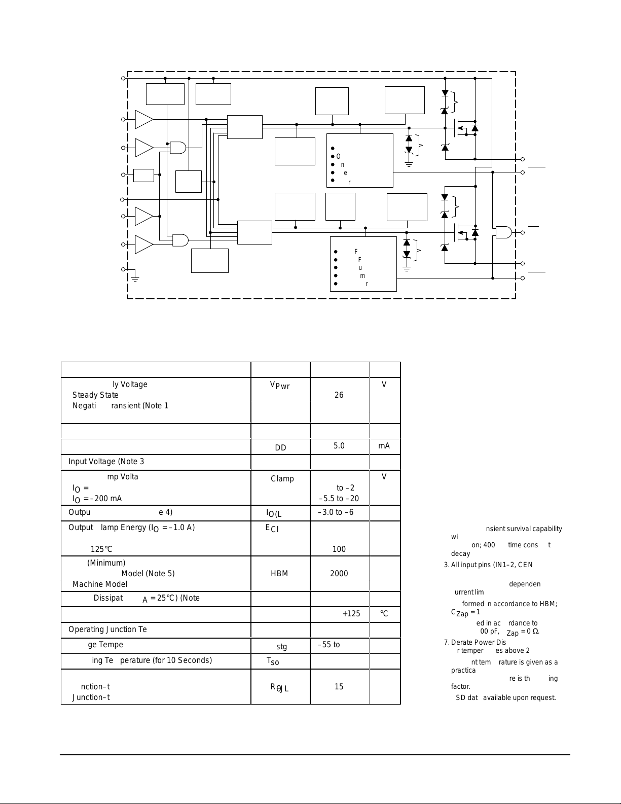
Figure 1. Simplified Internal Block Diagram
Voltage
Regulator
4.0 ms
Retry Timer
Gate
Control
Gate
Control
OFF/ON
Open Load
Detect
OFF/ON
Open Load
Detect
Current
Limit
Fault Detection
D
ON/OFF Open Load
D
ON/OFF V
D
On Ground Short
D
Over Temperature
D
V
Pwr
Current
Limit
Fault Detection
D
ON/OFF Open Load
D
ON/OFF V
D
On Ground Short
D
Over Temperature
D
V
Pwr
Short
Pwr
Overvoltage
Short
Pwr
Overvoltage
Over
T emperature
Shutdown
Over
T emperature
Shutdown
–10 V
–10 V
15 V
15 V
55 V
55 V
OUT1 (24)
(3)
STAT1
INT
(23)
OUT2 (13)
(10)
STAT2
MAXIMUM RATINGS (All voltages are with respect to ground, unless otherwise noted.)
Rating Symbol Value Unit
Power Supply Voltage
Steady State Continuous Operation 26
Negative Transient (Note 1) –1.5
Positive Load Dump Transient (Note 2) 60
Logic Supply Voltage Range
Logic Supply Current
Input Voltage (Note 3)
Output Clamp Voltage
IO = –20 mA –3.0 to –20
IO = –200 mA –5.5 to –20
Output Current Limit (Note 4)
Output Clamp Energy (IO = –1.0 A)
TJ = 25°C 300
TJ = 125°C 100
ESD (Minimum) V
Human Body Model (Note 5) HBM 2000
Machine Model (Note 6) MM 200
Power Dissipation (TA = 25°C) (Note 7)
Operating Temperature (Note 8)
Operating Junction Temperature
Storage Temperature
Soldering Temperature (for 10 Seconds)
Thermal Resistance
Junction–to–Lead R
Junction–to–Ambient R
V
Pwr
V
DD
I
DD
V
V
Clamp
I
O(Lim)
E
Clamp
P
T
T
T
stg
T
solder
θJL
θJA
–0.3 to 7.0
5.0
in
–0.3 to 7.0
–3.0 to –6.0
D
A
J
4.2
–40 to +125
–40 to +150
–55 to +150
270
°C/W
15
30
V
V
mA
V
V
A
mJ
W
°C
°C
°C
°C
NOTES: 1. Negative transient survival capability
for 100 ms time duration.
2.Positive transient survival capability
with typical automotive load dump
condition; 400 ms time constant
decay.
3.All input pins (IN1–2, CEN and
SFPD).
4.Each output has independent
current limiting.
5.Performed in accordance to HBM;
C
= 100 pF, R
Zap
6.Performed in accordance to MM;
C
= 100 pF, R
Zap
7.Derate Power Dissipation 33 mW/°C
for temperatures above 25°C.
8.Ambient temperature is given as a
practical reference; Maximum
junction temperature is the limiting
factor.
9.ESD data available upon request.
= 1500 Ω.
Zap
= 0 Ω.
Zap
2
MOTOROLA ANALOG IC DEVICE DATA

MC33143
ÁÁÁ
ÁÁÁ
Á
Á
Á
Á
Á
ÁÁÁ
Á
ÁÁÁ
ÁÁÁ
ÁÁÁ
ÁÁÁ
ÁÁÁ
ÁÁÁ
ÁÁÁ
ÁÁÁ
ÁÁÁ
ÁÁÁ
ÁÁÁ
DC ELECTRICAL CHARACTERISTICS (Characteristics noted under conditions 9.0 V ≤ V
≤ 17 V, 4.5 V ≤ VDD 5.5 V,
Pwr
–40°C ≤ TL ≤ 125°C, unless otherwise noted, typical values represent approximate mean at TL = 25°C.)
Characteristic
Symbol Min Typ Max Unit
POWER INPUT
Supply Voltage Range (Operational)
V
Pwr
9.0
–
17
Supply Current (Note 1)
Both Outputs ON
(CEN = IN1 = IN2 = 0.7 x VDD, IO1 = IO2 = –1.0 A) I
Standby (CEN = 0.7 x VDD, IN1 = IN2 = 0.3 x VDD, RL = 12 Ω) I
“Sleep State” (CEN = IN1 = IN2 = 0.3 x VDD, RL = 12 Ω) I
Logic Supply Voltage Range
БББББББББББББББББ
Logic Supply Current
Pwr
Pwr(sby)
Pwr(sleep)
V
DD
ÁÁÁ
I
DD
0.1 4.2 7.0 mA
– 3.9 7.0 mA
– 0.2 300 µA
4.5
ÁÁ
–
–
ÁÁ
0.43
5.5
ÁÁ
5.0
Both Outputs ON (IN1 = IN2 = 0.7 x VDD, IO1 = IO2 = –1.0 A) mA
Overvoltage Shutdown (Note 2)
Overvoltage Shutdown Hysteresis
NOTES: 1. Supply current when both outputs are ON and during standby are measured in the Ground pin while during “sleep state” is measured in the V
2.Overvoltage Shutdown causes enabled outputs to be forced OFF; Overvoltage fault is immediately reported.
DC ELECTRICAL CHARACTERISTICS (Characteristics noted under conditions 9.0 V ≤ V
V
Pwr(ovsd)
V
Pwr(hys)
30
0.3
≤ 17 V, 4.5 V ≤ VDD 5.5 V,
Pwr
33.2
0.5
38
1.5
–40°C ≤ TL ≤ 125°C, unless otherwise noted, typical values represent approximate mean at TL = 25°C.)
Characteristic
Symbol Min Typ Max Unit
POWER OUTPUT
Drain–to–Source ON Resistance (Note 1)
R
DS(on)
(TJ = 25°C, CEN = IN1 = IN2 = 0.7 x VDD)
IO = –0.5 A. V
IO = –1.0 A. V
IO = –2.0 A. V
Drain–to–Source ON Resistance (Note 1)
= 5.5 V – 0.2 0.5
Pwr
= 14 V – 0.14 0.2
Pwr
= 24 V – 0.14 0.2
Pwr
R
DS(on)
(TJ = 125°C, CEN = IN1 = IN2 = 0.7 x VDD)
IO = –0.5 A. V
IO = –1.0 A. V
IO = –2.0 A. V
Output Self–Limiting Current (Note 2)
= 5.5 V – – 1.0
Pwr
= 14 V – – 0.38
Pwr
= 24 V – – 0.38
Pwr
I
O(Lim)
–3.0
–4.1
–6.0
(CEN = IN1 = IN2 = SFPD = 0.7 x VDD, RL = 0 Ω)
Output OFF Leakage Current
I
O(Lkg)
–5.0
–45
–150
(CEN = 0.7 x VDD, IN1 = IN2 = 0.3 x VDD)
Output OFF Open Load Sense Current
I
O(Sense)
–5.0
–45
–150
(CEN = 0.7 x VDD, IN1 = IN2 = 0.3 x VDD)
Output ON Open Load Detection Current (Note 3)
I
O(On)
(CEN = IN1 = IN2 = 0.7 x VDD)
TL = –40°C –2.0 –145 –200
TL = 125°C –2.0 –181 –200
Output Clamp Voltage (Note 4)
V
Clamp
(CEN = 0.7 x VDD, IN1 = IN2 = 0.3 x VDD)
IO = –20 mA –9.0 –13.2 –20
IO = –200 mA –9.0 –13.5 –20
Over T emperature Shutdown Range (Note 5)
T
Lim
155
–
185
(CEN = IN1 = IN2 = SFPD = 0.7 x VDD)
Over Temperature Shutdown Hysteresis (Note 6)
NOTES: 1. R
2.Applies to each output; each output has independent self–limiting source current feature; Over Current and Short–to–Ground defined as condition
3.Applies to each output; tested for by ramping IO from 0 until STAT
4.Applies to each output; each output has independent dynamic output voltage clamping feature.
5.Applies to each output; each output has independent thermal shutdown; parameter is measured by ramping temperature until enabled output is
6.Parameter is established by design but is not production tested.
applies to OUT1, OUT2 and is independent of output current.
DS(on)
when output source current exceeds I
; Device ignores Over Current and Short–to–Ground faults from 0 to tss.
O(Lim)
≤ 0.7 x VDD; defined as the condition when IO is outside of I
disabled; parameter is established by design but is not production tested; thermal fault is immediately reported.
T
Lim(hys)
–
–
15
current window.
O(on)
V
V
ÁÁ
V
V
pin.
Pwr
Ω
Ω
A
µA
µA
mA
V
°C
°C
MOTOROLA ANALOG IC DEVICE DATA
3
 Loading...