

Device
Operating
Temperature Range
Package
SEMICONDUCTOR
TECHNICAL DATA
LOW VOLTAGE
COMPANDER
ORDERING INFORMATION
MC33110D
MC33110P
TA = –40 to 85°C
SO–14
Plastic DIP
P SUFFIX
PLASTIC PACKAGE
CASE 646
14
1
PIN CONNECTIONS
Order this document by MC33110/D
D SUFFIX
PLASTIC PACKAGE
CASE 751A
(SO–14)
14
1
V
CC
NC
V
ref
(Top View)
NC
Exp Filter
Exp Output
Exp Input
V
B
Gnd
Comp Filter
Comp Output
Comp Input
Inv Input
Comp Feedback
1
2
3
4
14
13
12
11
5
6
7
10
9
8
1
MOTOROLA RF/IF DEVICE DATA
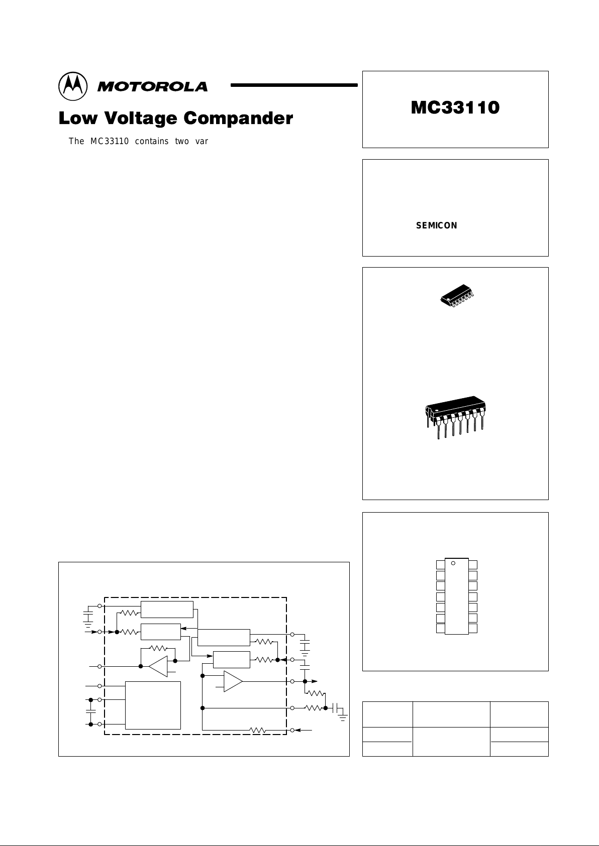
The MC33110 contains two variable gain circuits configured for
compressing and expanding the dynamic range of an audio signal. One
circuit is configured as an expander, while the other circuit can be configured
as a compressor or expander. Each circuit has a full wave rectifier to provide
average value information to a variable gain cell located in either the input
stage or the feedback path. An internal, temperature stable bandgap
reference provides the necessary precision voltages and currents required.
The MC33110 will operate from a supply voltage of 2.1 to 7.0 V, over a
temperature range of –40 to 85°C. The device is designed to accommodate
an 80 dB dynamic range from –60 dB to 20 dB, referenced to 100 mVrms.
Applications include cordless telephone, CB, walkie–talkie, most voice
RF links, and any application where the signal–to–noise ratio can be
improved by reducing the transmitted dynamic range. Other applications
include speakerphone and voice activated intercom, dictating machine,
standard telephone, etc.
The MC33110 is packaged in a 14 pin DIP for through–the–hole
applications and an SO–14 surface mount.
• Operating Supply Voltage: 2.1 to 7.0 V
• No Precision External Components Required
• 80 dB Dynamic Range Compressed to 40 dB, Re–expandable to 80 dB
• Unity Gain Level: 100 mVrms
• Adjustable Response Time
• Ambient Operating Temperature: –40 to 85°C
• Temperature Compensated Reference
• Applications Include Cordless Phone, CB Radio, Speakerphone, etc.
Simplified Block Diagram
+
–
+
–
2.2 µF
14
3
5
4
6
7
Gnd
10
µ
F
V
B
V
CC
Exp.
Output
Exp
Input
4.7 k
10 k
Rectifier
∆
Gain
10 k
V
B
Bias
&
Reference
Generator
V
B
∆
Gain
Rectifier
4.7 k
10 k
12
8
11
9
10
Comp
Input
1.0
µ
F
20 k
20 k
Comp
Output
2.0
µ
F
2.2
µ
F
10 k
Motorola, Inc. 1998 Rev 1
MC33110
2
MOTOROLA RF/IF DEVICE DATA
PIN DESCRIPTION
Name Pin Description
V
ref
1 Normally this pin is not used and is left open. It can be used to make limited adjustments to
the 0 dB level. Any noise or leakage at this pin will affect the 0 dB level and gain tracking.
NC 2, 13 No connection. These pins are not internally connected.
Expander Filter 3 Connect to an external capacitor to filter the full wave rectifier’s output. This capacitor
affects attack and decay times, as well as low frequency accuracy.
Expander Output 4 Output of the expander amplifier.
Expander Input 5 The input impedance is nominally 3.2 kΩ. Nominal signal range is 3.16 mVrms to
316 mVrms. Must be capacitor coupled to the signal source.
V
B
6 An internal reference voltage, nominally VCC/2. This is an ac ground and must be well
filtered to obtain high power supply rejection and low crosstalk.
Ground 7 Connect to a clean power supply ground.
Compressor Feedback 8 Input to the compressor variable gain stage and rectifier. Normally the signal is supplied by
the compressor’s output (Pin 11). Input impedance is nominally 3.2 kΩ.
Inverting Input 9 Inverting input to the compressor amplifier. Normally, this is connected to the compressor’s
output through a filtered dc feedback path.
Compressor Input 10 The input impedance is nominally 10 kΩ. Nominal signal range is 100 µVrms to 1.0 Vrms.
Must be capacitor coupled to the signal source.
Compressor Output 11 Output of the compressor amplifier.
Compressor Filter 12 Connect to an external capacitor to filter the full wave rectifier’s output. This capacitor
affects attack & decay times, and low frequency accuracy.
V
CC
14 Power supply pin. Connect to a power supply providing between 2.1 V and 7.0 V . Nominal
current consumption is 3.5 mA.
1.0 V
100 mV
100
µ
V
1.0 mV
10 mV
316 mV
31.6 mV
10 mV
3.16 mV
+
–
+
–
Rectifier
∆
Gain
I
ref
V
B
R6
R5
V
out
R4
V
in
– 60 dB
– 50 dB
– 40 dB
– 30 dB
– 20 dB
– 10 dB
0 dB
10 dB
20 dB
V
in
R2
R1
∆
Gain
Rectifier
I
ref
R
S
V
B
V
out
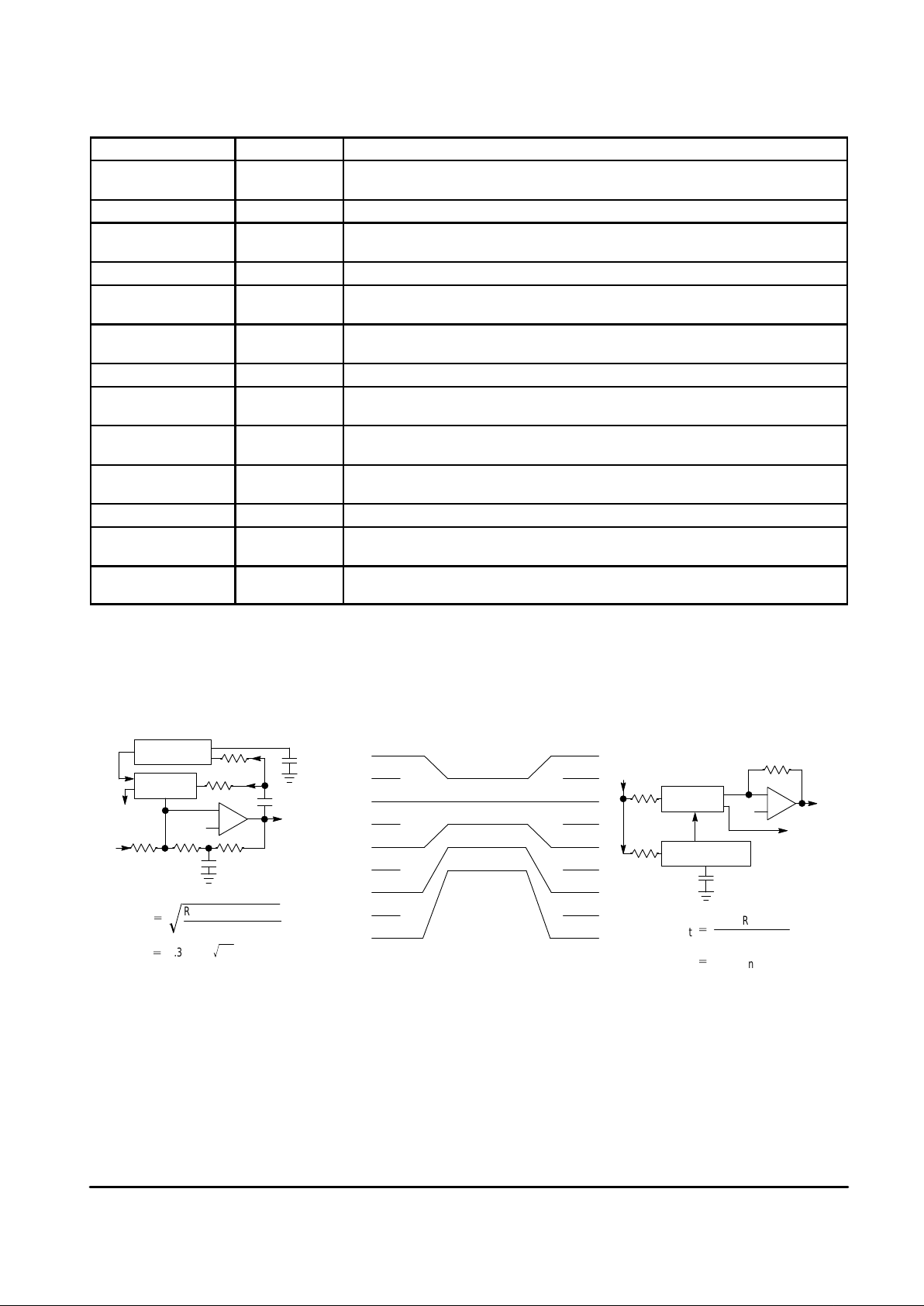
Transfer FunctionsCompressor Expander
Compression Expansion
(Voltages are rms)
V
out
+
R5 x R6 x I
refxVin
7.2 x R4
Ǹ
+
0.3162 x V
in
Ǹ
V
out
+
7.2 x R3 x V
in
2
R1xR2xI
ref
+
10 x V
in
2
MC33110
3
MOTOROLA RF/IF DEVICE DATA
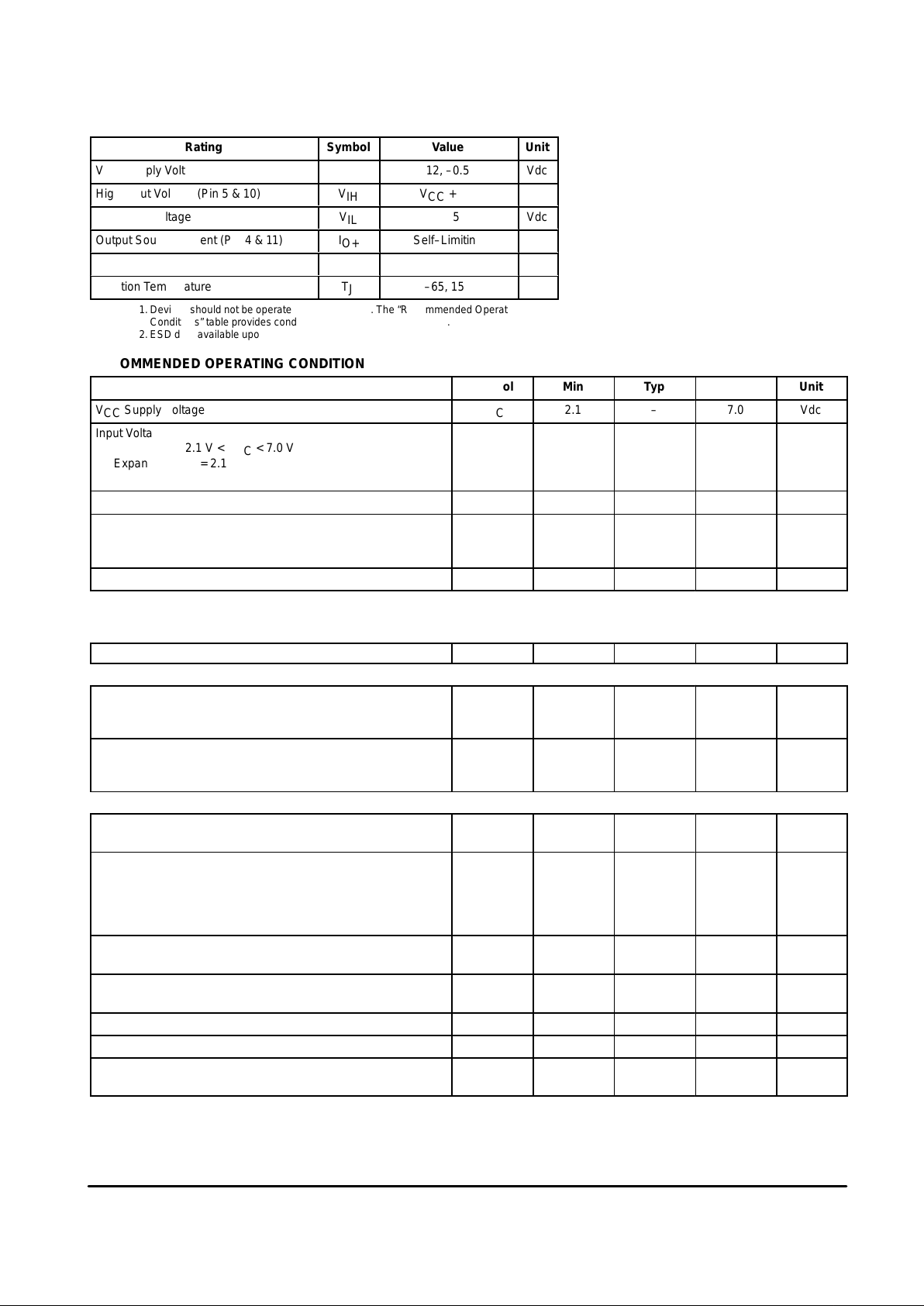
MAXIMUM RATINGS
Rating
Symbol
Value
Unit
VCC Supply Voltage
V
CC
12, –0.5
Vdc
High Input Voltage (Pin 5 & 10)
V
IH
VCC + 0.5
Vdc
Low Input Voltage
V
IL
–0.5
Vdc
Output Source Current (Pin 4 & 11)
I
O+
Self–Limiting
Output Sink Current
I
O–
20
mA
Junction Temperature
T
J
–65, 150
°C
NOTES: 1. Devices should not be operated at these values. The “Recommended Operating
Conditions” table provides conditions for actual device operation.
2.ESD data available upon request.
RECOMMENDED OPERATING CONDITIONS
Characteristic Symbol Min Typ Max Unit
VCC Supply Voltage V
CC
2.1 – 7.0 Vdc
Input Voltage Range
Compressor, 2.1 V < VCC < 7.0 V
Expander, VCC = 2.1 V
Expander, 3.0 V < VCC < 7.0 V
V
IR
0
0
0
–
–
–
1.0
0.25
0.316
Vrms
Input Frequency F
in
100 – 20 k Hz
Output Load
Compressor (Pin 11, VO = 100 mV)
Expander (Pin 4, VO = 100 mV)
R
L
300
150
–
–
∞
∞
Ω
Ambient Temperature T
A
–40 – 85 °C
All limits are not necessarily functional concurrently.
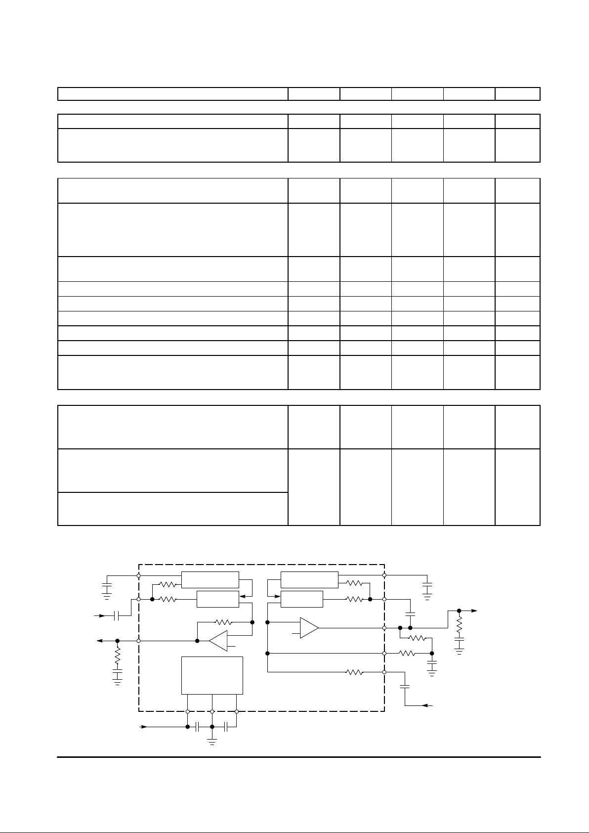
ELECTRICAL CHARACTERISTICS (V
CC
= 5.0 V , f = 1.0 kHz, unless otherwise noted, TA = 25°C, see Figure 1)
Characteristic
Symbol Min Typ Max Unit
POWER SUPPLY
Power Supply Current
VCC = 5.0 V
VCC = 2.1 V
I
CC
–
–
3.5
3.3
5.5
–
mA
VB Voltage
VCC = 5.0 V
2.1 V < VCC < 7.0 V
V
B
2.4
–
2.5
VCC/2
2.6
–
Vdc
COMPRESSOR
0 dB Gain
Vin = 100 mVrms, Pin 1 = Open
G
(CO)
–1.5 0 1.5
dB
Gain Tracking
@ Vin = 1.0 Vrms, output relative to G
(CO)
@ Vin = 10 mVrms, output relative to G
(CO)
@ Vin = 1.0 mVrms, output relative to G
(CO)
@ Vin = 100 µVrms, output relative to G
(CO)
G
t
9.0
–
–
–31
10
–10
–20
–30
11
–
–
–29
dB
Total Harmonic Distortion
Vin = 100 mVrms, f = 1.0 kHz
THD
0 0.1 1.5
%
Power Supply Rejection
f = 1.0 kHz, CVB = 10 µF, Vin = – 20 dB
PSRR
– 22 –
dB
Attack Time (Capacitor @ Pin 12 = 2.2 µF) t
a(C)
– 6.0 – ms
Decay Time (Capacitor @ Pin 12 = 2.2 µF) t
d(C)
– 20 – ms
Input Impedance Pin 10
Pin 8
R
in
–
–
10
3.2
–
–
kΩ
MC33110
4
MOTOROLA RF/IF DEVICE DATA
ELECTRICAL CHARACTERISTICS
(VCC = 5.0 V , f = 1.0 kHz, unless otherwise noted, TA = 25°C, see Figure 1)
Characteristic UnitMaxTypMinSymbol
COMPRESSOR
Peak Output Current Pin 11 I
pk
– 0.3 – mA
Output Offset
Pin 11, with respect to Pin 6, NO SIGNAL
Change from NO SIGNAL to 1.0 Vrms at Input
V
OO
–150
–
0
50
150
–
mVdc
EXPANDER
0 dB Gain
(Vin = 100 mVrms, Pin 1 = open)
G
(EO)
–1.5 0 1.5
dB
Gain Tracking
@ Vin = 316 mVrms, output relative to G
(EO)
@ Vin = 31.6 mVrms, output relative to G
(EO)
@ Vin = 10 mVrms, output relative to G
(EO)
@ Vin = 3.16 mVrms, output relative to G
(EO)
G
t
19
–
–
–61
+ 20
– 20
– 40
– 60
21
–
–
–59
dB
Total Harmonic Distortion
Vin = 100 mVrms, f = 1.0 kHz
THD
0 0.06 1.5
%
Power Supply Rejection (f = 1.0 kHz, CVB = 10 µF) PSRR – 37 – dB
Attack Time (Capacitor @ Pin 3 = 2.2 µF) t
a(E)
– 19 – ms
Decay Time (Capacitor @ Pin 3 = 2.2 µF) t
d(E)
– 20 – ms
Input Impedance Pin 5 R
in
– 3.2 – kΩ
Peak Output Current Pin 4 I
pk
– 1.0 – mA
Output Offset
Pin 4, with respect to Pin 6, NO SIGNAL
Change from NO SIGNAL to 316 mVrms at Input
V
OO
–150
–
0
25
150
–
mVdc
MISCELLANEOUS
Gain (Pin 10 to Pin 4; Pin 11 capacitor coupled to Pin 5)
VCC = 7.0 V , Vin = 1.0 Vrms
VCC = 3.0 V , Vin = 1.0 Vrms
VCC = 2.1 V , Vin = 31.6 mVrms
A
V
–2.5
–2.5
–2.5
0
0
0
2.5
2.5
2.5
dB
Channel Separation
Expander to Compressor, output measured at Pin 11
Vin @ Pin 5 = 316 mVrms, f = 1.0 kHz
Vin @ Pin 5 = 316 mVrms, f = 10 kHz
CS
43
–
48
68
–
–
dB
Compressor to Expander, output measured at Pin 4
Vin @ Pin 10 = 1.0 Vrms, f = 1.0 kHz
Vin @ Pin 10 = 1.0 Vrms, f = 10 kHz
65
–
107
114
–
–
Figure 1. Test Circuit
+
–
+
–
2.2 µF
2 µF
5.0 k
3.0
µ
F
Expander
Input
Expander
Output
V
CC
4.7
µ
F 4.7 µF
14 7 6
3
5
4
4.7 k
10 k
Rectifier
∆
Gain
Rectifier
∆
Gain
V
B
V
B
10 k
V
B
Bias &
Reference
Generator
4.7 k
10 k
10 k
12
8
11
9
10
2.0
µ
F
1.0 µF
3.0
µ
F
5.0 k
2.2
µ
F
Compressor
Output
1.0
µ
F
Compressor
Input
10 k
10 k
 Loading...