Motorola MC33102P, MC33102D Datasheet

Order this document by MC33102/D
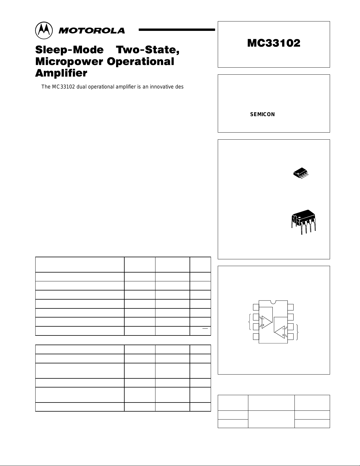
The MC33102 dual operational amplifier is an innovative design concept
employing Sleep–Mode technology. Sleep–Mode amplifiers have two
separate states, a sleepmode and an awakemode. In sleepmode, the
amplifier is active and waiting for an input signal. When a signal is applied
causing the amplifier to source or sink 160 µA (typically) to the load, it will
automatically switch to the awakemode which offers higher slew rate, gain
bandwidth, and drive capability.
• Two States: “Sleepmode” (Micropower) and “A wakemode”
(High Performance)
• Switches from Sleepmode to Awakemode in 4.0 µs when Output Current
Exceeds the Threshold Current (RL = 600 Ω)
• Independent Sleepmode Function for Each Op Amp
• Standard Pinouts – No Additional Pins or Components Required
• Sleepmode State – Can Be Used in the Low Current Idle State as a
Fully Functional Micropower Amplifier
• Automatic Return to Sleepmode when Output Current Drops Below
Threshold
• No Deadband/Crossover Distortion; as Low as 1.0 Hz in the Awakemode
• Drop–in Replacement for Many Other Dual Op Amps
• ESD Clamps on Inputs Increase Reliability without Affecting Device
Operation
Sleep–Mode is a trademark of Motorola, Inc.
TYPICAL SLEEPMODE/AWAKEMODE PERFORMANCE
Characteristic
Low Current Drain 45 750 µA
Low Input Offset Voltage 0.15 0.15 mV
High Output Current Capability 0.15 50 mA
Low T.C. of Input Offset Voltage 1.0 1.0 µV/°C
High Gain Bandwidth (@ 20 kHz) 0.33 4.6 MHz
High Slew Rate 0.16 1.7 V/µs
Low Noise (@ 1.0 kHz) 28 9.0
Sleepmode
(Typical)
MAXIMUM RATINGS
Ratings Symbol Value Unit
Supply Voltage (VCC to VEE) V
Input Differential Voltage Range
Input Voltage Range
Output Short Circuit Duration (Note 2) t
Maximum Junction Temperature
Storage Temperature
Maximum Power Dissipation P
NOTES: 1. Either or both input voltages should not exceed VCC or VEE.
2.Power dissipation must be considered to ensure maximum junction temperature (TJ)
is not exceeded (refer to Figure 1).
V
IDR
V
SC
T
T
S
IR
J
stg
D
Awakemode
(Typical) Unit
+36 V
(Note 1) V
(Note 2) sec
+150
–65 to +150
(Note 2) mW
nV/ Hz√
°C
DUAL SLEEP–MODE
OPERATIONAL AMPLIFIER
SEMICONDUCTOR
TECHNICAL DATA
D SUFFIX
PLASTIC PACKAGE
CASE 751
(SO–8)
P SUFFIX
PLASTIC PACKAGE
CASE 626
PIN CONNECTIONS
Inputs 1
V
EE
ORDERING INFORMATION
Device
MC33102D
MC33102P
Temperature Range
TA = – 40° to +85°C
1Output 1 V
2
1
3
4
(Dual, Top View)
Operating
8
1
8
1
8
CC
Output 2
7
6
2
5
Plastic DIP
Inputs
2
Package
SO–8
MOTOROLA ANALOG IC DEVICE DATA
Motorola, Inc. 1996 Rev 0
1

MC33102
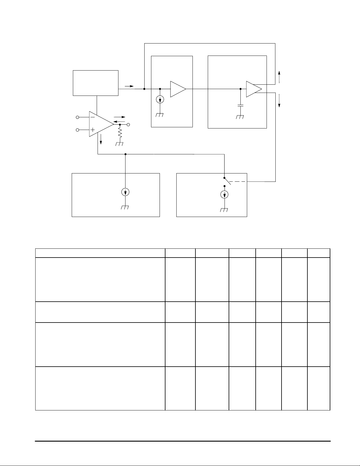
Simplified Block Diagram
V
in
Fractional
Load Current
Detector
Op Amp
I
Bias
Sleepmode
Current
Regulator
Current
Threshold
Detector
% of I
L
Buffer Buffer
I
I
L
V
out
R
L
I
sleep
ref
Awakemode
Current
Regulator
Awake to
Sleepmode
Delay Circuit
C
Storage
I
awake
Enable
I
Hysteresis
I
Enable
DC ELECTRICAL CHARACTERISTICS (V
Characteristics
Input Offset Voltage (RS = 50 Ω, VCM = 0 V, VO = 0 V)
Sleepmode
TA = +25°C
TA = –40° to +85°C
Awakemode
TA = +25°C
TA = –40° to +85°C
Input Offset Voltage Temperature Coefficient
(RS = 50 Ω, VCM = 0 V, VO = 0 V)
TA = –40° to +85°C (Sleepmode and Awakemode)
Input Bias Current (VCM = 0 V, VO = 0 V)
Sleepmode
TA = +25°C
TA = –40° to +85°C
Awakemode
TA = +25°C
TA = –40° to +85°C
Input Offset Current (VCM = 0 V, VO = 0 V)
Sleepmode
TA = +25°C
TA = –40° to +85°C
Awakemode
TA = +25°C
TA = –40° to +85°C
CC
= +15 V, VEE = –15 V, TA = 25°C, unless otherwise noted.)
Figure Symbol Min Typ Max Unit
2 VIO
3 ∆VIO/∆T
4, 6 I
— IIO
IB
—
—
—
—
— 1.0 —
—
—
—
—
—
—
—
—
0.15
—
0.15
—
8.0
—
100
—
0.5
—
5.0
—
mV
2.0
3.0
2.0
3.0
µV/°C
nA
50
60
500
600
nA
5.0
6.0
50
60
2
MOTOROLA ANALOG IC DEVICE DATA

MC33102
DC ELECTRICAL CHARACTERISTICS (V
Characteristics
Common Mode Input Voltage Range
(∆VIO = 5.0 mV, VO = 0 V)
Sleepmode and Awakemode
Large Signal Voltage Gain
Sleepmode (RL = 1.0 MΩ)
TA = +25°C
TA = –40° to +85°C
Awakemode (VO = ±10 V, RL = 600 Ω)
TA = +25°C
TA = –40° to +85°C
Output Voltage Swing (VID = ±1.0 V)
Sleepmode (VCC = +15 V, VEE = –15 V)
RL = 1.0 MΩ
RL = 1.0 MΩ
Awakemode (VCC = +15 V, VEE = –15 V)
RL = 600 Ω
RL = 600 Ω
RL = 2.0 kΩ
RL = 2.0 kΩ
Awakemode (VCC = +2.5 V, VEE = –2.5 V)
RL = 600 Ω
RL = 600 Ω
Common Mode Rejection (VCM = ±13 V)
Sleepmode and Awakemode
Power Supply Rejection (VCC/VEE = +15 V/–15 V,
5.0 V/–15 V , +15 V/–5.0 V)
Sleepmode and Awakemode
Output Transition Current
Sleepmode to Awakemode (Source/Sink)
(VS = ±15 V)
(VS = ±2.5 V)
Awakemode to Sleepmode (Source/Sink)
(VS = ±15 V)
(VS = ±2.5 V)
Output Short Circuit Current (Awakemode)
(VID = ±1.0 V , Output to Ground)
Source
Sink
Power Supply Current (per Amplifier) (ACL = 1, VO = 0V)
Sleepmode (VS = ±15 V)
TA = +25°C
TA = –40° to +85°C
Sleepmode (VS = ±2.5 V)
TA = +25°C
TA = –40° to +85°C
Awakemode (VS = ±15 V)
TA = +25°C
TA = –40° to +85°C
= +15 V, VEE = –15 V, TA = 25°C, unless otherwise noted.)
CC
Figure Symbol Min Typ Max Unit
5 V
7 A
8, 9, 10
11 CMR
12 PSR
13, 14
15, 16 ISC
17 I
I
I
ICR
VOL
V
V
V
V
V
V
V
O+
V
TH1
TH2
O+
O–
O+
O–
O+
O–
O–
–13
—
25
15
50
25
+13.5
—
+12.5
—
+13.3
—
+1.1
—
80 90 —
80 100 —
200
250
—
—
50
50
D
—
—
—
—
—
—
–14.8
+14.2
200
—
700
—
+14.2
–14.2
+13.6
–13.6
+14
–14
+1.6
–1.6
160
200
142
180
110
110
45
48
38
42
750
800
—
+13
—
—
—
—
—
–13.5
—
–12.5
—
–13.3
—
–1.1
—
—
90
140
—
—
65
70
65
—
800
900
V
kV/V
V
V
dB
dB
µA
mA
µA
MOTOROLA ANALOG IC DEVICE DATA
3

MC33102
AC ELECTRICAL CHARACTERISTICS
Characteristics
Slew Rate (Vin = –5.0 V to +5.0 V, CL = 50 pF, AV = 1.0)
Sleepmode (RL = 1.0 MΩ)
Awakemode (RL = 600 Ω)
Gain Bandwidth Product
Sleepmode (f = 10 kHz)
Awakemode (f = 20 kHz)
Sleepmode to Awakemode Transition T ime
(ACL = 0.1, Vin = 0 V to +5.0 V)
RL = 600 Ω
RL = 10 kΩ
Awakemode to Sleepmode Transition T ime 22 t
Unity Gain Frequency (Open Loop)
Sleepmode (RL = 100 kΩ, CL = 0 pF)
Awakemode (RL = 600 Ω, CL = 0 pF)
Gain Margin
Sleepmode (RL = 100 kΩ, CL = 0 pF)
Awakemode (RL = 600 Ω, CL = 0 pF)
Phase Margin
Sleepmode (RL = 100 kΩ, CL = 0 pF)
Awakemode (RL = 600 Ω, CL = 0 pF)
Channel Separation (f = 100 Hz to 20 kHz)
Sleepmode and Awakemode
Power Bandwidth (Awakemode)
(VO = 10 Vpp, RL = 100 kΩ, THD ≤ 1%)
Total Harmonic Distortion (VO = 2.0 Vpp, AV = 1.0)
Awakemode (RL = 600 Ω)
f = 1.0 kHz
f = 10 kHz
f = 20 kHz
DC Output Impedance (VO = 0 V, AV = 10, IQ = 10 µA)
Sleepmode
Awakemode
Differential Input Resistance (VCM = 0 V)
Sleepmode
Awakemode
Differential Input Capacitance (VCM = 0 V)
Sleepmode
Awakemode
Equivalent Input Noise V oltage (f = 1.0 kHz, RS = 100 Ω)
Sleepmode
Awakemode
Equivalent Input Noise Current (f = 1.0 kHz)
Sleepmode
Awakemode
(V
= +15 V, VEE = –15 V, TA = 25°C, unless otherwise noted.)
CC
Figure Symbol Min Typ Max Unit
18 SR
19 GBW
20, 21 t
23, 25 A
24, 26 ∅
29 CS
30 THD
31 R
32 e
33 i
f
BW
R
C
tr1
tr2
0.10
1.0
0.25
3.5
—
—
— 1.5 — sec
U
M
M
P
O
in
in
n
n
—
—
—
—
—
—
— 120 —
— 20 —
—
—
—
—
—
—
—
—
—
—
—
—
—
0.16
1.7
0.33
4.6
4.0
15
200
2500
13
12
60
60
0.005
0.016
0.031
1.0 k
96
1.3
0.17
0.4
4.0
28
9.0
0.01
0.05
—
—
—
—
—
—
—
—
—
—
—
—
—
—
—
—
—
—
—
—
—
—
—
—
—
V/µs
MHz
µs
kHz
dB
Degrees
dB
kHz
%
Ω
MΩ
pF
nV/ Hz√
pA/ Hz√
4
MOTOROLA ANALOG IC DEVICE DATA

MC33102
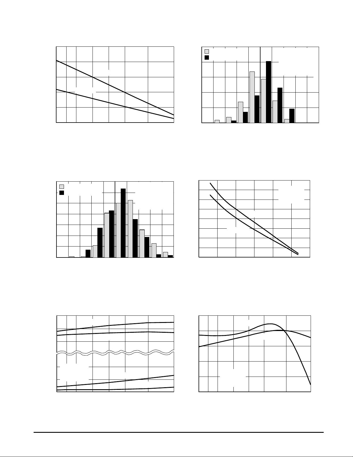
Figure 1. Maximum Power Dissipation
versus T emperature
2500
2000
1500
1000
500
, MAXIMUM POWER DISSIPATION (mW)
D(max)
P
0
–55 –25 0 25 50 12585–40
MC33102D
MC33102P
TA, AMBIENT TEMPERATURE (°C)
Figure 3. Input Offset V oltage Temperature
Coefficient Distribution (MC33102D Package)
35
Percent Sleepmode
30
Percent Awakemode
25
20
15
10
PERCENT OF AMPLIFIERS (%)
5.0
0
–5.0 –15 –10 –5.0 0 5.0 1510
–4.0 –3.0 –2.0 –1.0 0 1.0 2.0 3.0 4.0 5.0
TCVIO, INPUT OFFSET VOLTAGE TEMPERATURE COEFFICIENT (µV/°C)
204 Amplifiers tested
from 3 wafer lots.
VCC = +15 V
VEE = –15 V
°
TA = –40
C to 85°C
Figure 2. Distribution of Input Offset Voltage
(MC33102D Package)
50
Percent Sleepmode
Percent Awakemode
40
30
20
PERCENT OF AMPLIFIERS (%)
10
0
–1.0
–0.8 –0.6 –0.4 –0.2 0 0.2 0.4 0.6 0.8 1.0
VIO, INPUT OFFSET VOLTAGE (mV)
Figure 4. Input Bias Current versus
Common Mode Input Voltage
10.5
9.5
8.5
7.5
, SLEEPMODE INPUT BIAS CURRENT (nA)
IB
6.5
I
Awakemode
VCM, COMMON MODE INPUT VOLTAGE (V)
Sleepmode
204 Amplifiers tested
from 3 wafer lots.
VCC = +15 V
VEE = –15 V
°
C
TA = 25
100
VCC = +15 V
VEE = –15 V
TA = 25
90
°
C
80
70
60
, AWAKEMODE INPUT BIAS CURRENT (nA)
IB
I
Figure 5. Input Common Mode V oltage Range
versus T emperature
V
CC
VCC–0.5
VCC–1.0
VEE+1.0
VEE+0.5
, INPUT COMMON MODE VOL TAGE RANGE (V)
ICR
V
VCC = +15 V
VEE = –15 V
∆
VIO = 5.0 mV
V
EE
–55 –25 0 25 50 85 125
–40
Sleepmode
Awakemode
Awakemode
TA, AMBIENT TEMPERATURE (°C)
MOTOROLA ANALOG IC DEVICE DATA
Sleepmode
Figure 6. Input Bias Current versus T emperature
10.0
Sleepmode
8.0
6.0
4.0
2.0
, SLEEPMODE INPUT BIAS CURRENT (nA)
IB
I
0
–55 –25 0 25 50 85 125–40
VCC = +15 V
VEE = –15 V
VCM = 0 V
TA, AMBIENT TEMPERATURE (°C)
Awakemode
100
80
60
40
20
0
, AWAKEMODE INPUT BIAS CURRENT (nA)
IB
I
5
 Loading...