Motorola MC33092ADW Datasheet

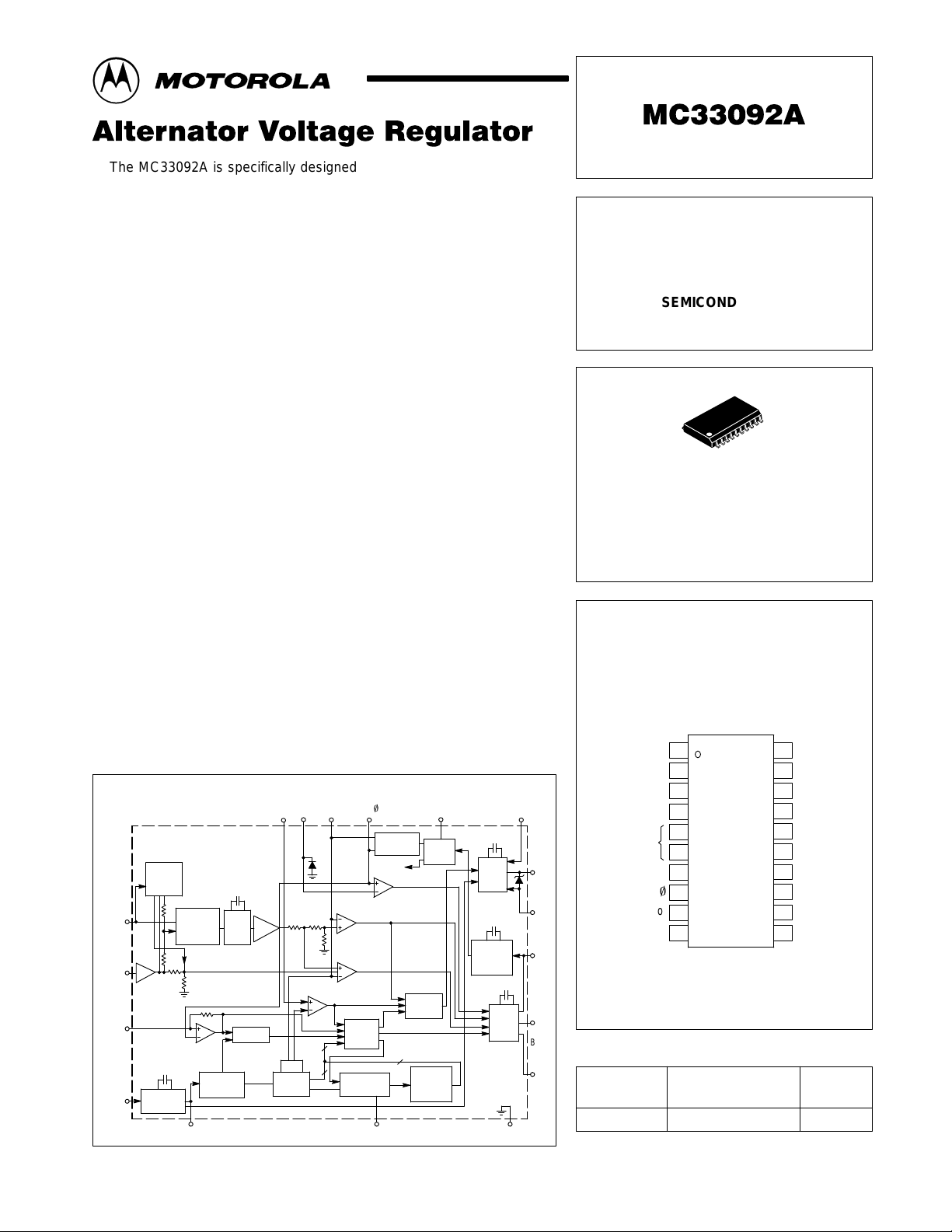
The MC33092A is specifically designed for voltage regulation and Load
Response Control (LRC) of diode rectified alternator charging systems, as
commonly found in automotive applications. The MC33092A provides load
response control of the alternator output current to eliminate engine speed
hunting and vibration due to sudden electrical loads which cause abrupt
torque loading of the engine at low RPM. Two load response rates are
selectable using Pin 11. The timing of the response rates is dependent on
the oscillator frequency .
In maintaining system voltage, the MC33092A monitors and compares
the system battery voltage to an externally programmed set point value and
pulse width modulates an N–channel MOSFET transistor to control the
average alternator field current.
• Forced Load Response Control (LRC) with Heavy Load Transitions
at Low RPM
• Capable of Regulating Voltage to ± 0.1 V @ 25°C
• Operating Frequency Selectable with One External Resistor
• < 0.1 V V ariation over Speed Range of 2000 to 10,000 RPM
• < 0.4 V V ariation over 10% to 95% of Maximum Alternator Output
• Maintains Regulation with External Loads as Low as 1.0 A
• Load Dump Protection of Lamp, Field Control Devices, and Loads
• Duty Cycle Limit Protection
• Provides High Side MOSFET Control of a Ground Referenced Field
Winding
• Controlled MOSFET and Flyback Diode Recovery Characteristics for
Minimum RFI
• < 2.0 mA Standby Current from Battery @ 25°C
• < 3.0 mA Standby Current from Battery Over Temperature Range
• Optional 2.5 or 10 sec. LRC Rate Control (Osc. Freq. = 280 kHz)
• Undervoltage, Overvoltage and Phase Fault (Broken Belt) Detection
Order this document by MC33092A/D
ALTERNATOR VOLTAGE
REGULATOR
SEMICONDUCTOR
TECHNICAL DATA
20
1
DW SUFFIX
PLASTIC PACKAGE
CASE 751D
(SO–20L)
PIN CONNECTIONS
Simplified Block Diagram
Sense
(Remote)
12
Supply
Reg
(Local)
10
Phase
Osc.
Adjust
2
7
Sense
Circuit
X1
Oscillator
FB UV V
1 19 20 8 14 13
MC33092A
Lost
Signal
Combiner
and Switch
Oscillator
Low
Pass
Buff
Filter
Counter
Prescaler
(24)
911
Counter
DAC
(28)
ref
Regulate
12
4
MOTOROLA ANALOG IC DEVICE DATA
O
V
ref
Bandgap
Reference
Bias
Undervoltage
Load Dump
Overvoltage
Control
Logic
Divide By
(1/12/48)
Rate
VCC1V
Power
8
Supply
Output
Control
Up/Down
Counter
(24)
Charge
Power
Up/Down
Circuit
Pump
Lamp
Control
Logic
Gnd
CC
156
3
17
18
Source
3
Lamp
Coll.
4
Lamp
Base
5
Gnd
Gnd
Adjust
V
ref
1
2
3
4
5
6
7
O
8
9
Filter Buffer
Remote Sense
Lamp Collector
Lamp Base
Oscillator
Gate
Oscillator
Phase
(Top View)
ORDERING INFORMATION
Operating
Device
MC33092ADW TA = – 35° to +125°C SO–20L
Motorola, Inc. 1997 Rev 0
Temperature Range
V
20
ref
Undervoltage
19
Source
18
Gate
17
NC
16
Gnd
15
VCC1
14
VCC3
13
Supply
12
Regulation
1110
Rate
Package
1

MAXIMUM RATINGS
Rating Symbol Value Unit
Power Supply Voltage V
Load Dump Transient V oltage (Note 1) +V
Negative Voltage (Note 2) –V
Power Dissipation and Thermal Characteristics
Maximum Power Dissipation @ TA = 125°C P
Thermal Resistance, Junction–to–Ambient R
Operating Junction Temperature T
Operating Ambient Temperature Range T
Storage Temperature Range T
NOTE: ESD data available upon request.
MC33092A
bat
max
min
D
θJA
J
A
stg
24 V
40 V
–2.5 V
867 mW
75 °C/W
+150 °C
–35 to +125 °C
–45 to +150 °C
ELECTRICAL CHARACTERISTICS (External components per Figure 1, T
Characteristic Symbol Min Typ Max Unit
DC CHARACTERISTICS
Regulation Voltage V
(Determined by external resistor divider)
Regulation Voltage Temperature Coefficient T
Suggested Battery Voltage Operating Range V
Power Up/Down Threshold Voltage (Pin 3) V
Standby Current,
V
= 12.8 V, Ignition off, TA = 25°C I
bat
V
= 12.8 V, Ignition off, –35°C ≤ TA ≤ 125°C I
bat
Zero Temperature Coefficient Reference Voltage, (Pin 8) V
Band Gap Reference Voltage (Pin 20) V
Band Gap Reference Temperature Coefficient TC –13 –11 – 9.0 mV/°C
Sense Loss Threshold (Pin 2) S
Phase Detection Threshold Voltage (Pin 10) P
Phase Rotation Detection Frequency (Pin 10) P
Undervoltage Threshold (Pin 19) V
Overvoltage Threshold (Pin 2, or Pin 12 if Pin 2 is not used) V
Load Dump Threshold (Pin 2, or Pin 12 if Pin 2 is not used) V
SWITCHING CHARACTERISTICS
Fundamental Regulation Output Frequency, (Pin 17)
(Clock oscillator frequency divided by 4096)
Suggested Clock Oscillator Frequency Range, (Pin 9) f
(Determined by external resistor, RT, see Figure 6)
Duty Cycle (Pin 17)
At Start–up Start
During Overvoltage Condition OV
Low/High RPM Transition Frequency (Pin 10) LRC
LRC Duty Cycle Increase Rate
Low RPM Mode (LRC
Pin 11 = Open (Slow Rate)
Low RPM Mode (LRC
Pin 11 = Grounded (Fast Rate)
High RPM Mode (LRC
Pin 11 = Don’t Care (LRC Mode is disabled)
NOTES: 1. 125 ms wide square wave pulse.
2.Maximum time = 2 minutes.
< 247 Hz), LRC
Freq
< 247 Hz), LRC
Freq
> 309 Hz), LRC
Freq
Loss(th)
= 25°C, unless otherwise noted).
A
Reg
C
bat
Pwr
Q1
Q2
O
ref
ref
Th
Rot
UV
OV
LD
f – 68 – Hz
osc
DC
DC
Freq
S
F
H
– 14.85 – V
–13 –11 – 9.0 mV/°C
11.5 14.85 16.5 V
0.5 1.2 2.0 V
– 1.3 2.0 mA
– – 3.0 mA
1.1 1.25 1.4 V
1.7 2.0 2.3 V
– 0.6 1.0 V
1.0 1.25 1.5 V
– 36 – Hz
1.0 1.25 1.5 V
1.09(V
1.33(V
) 1.12(V
ref
) 1.4(V
ref
205 280 350 kHz
27 29 31 %
3.5 4.7 5.5 %
247 273 309 Hz
8.5 9.5 10.5 %/sec
34 38 42 %/sec
409 455 501 %/sec
) 1.16(V
ref
) 1.48(V
ref
) V
ref
) V
ref
2
MOTOROLA ANALOG IC DEVICE DATA

MC33092A
Sense
Phase
B+ Supply
3
CC
V
1.0 k
1
CC
V
250
O
ref
V
MTB36N06E
(Q1)
13
14
Power
Bandgap
Reference
8
17
Charge
Supply
Bias
Field
2.0 k
20 k
18
Gate
Pump
Undervoltage
Source
Ignition
Lamp
2.0 k
3
Power
Up/Down
Lamp
Collector
Circuit
500
BSP52T1
(Q2)
Output
Control
4
Lamp
Control
Lamp
Base
Logic
8
Stator
5
Up/Down
10
Ground
)
4
(2
Counter
Battery
MR850
Ground 6 and 1511
Ground
Rate
Configuration
Alternate Stator
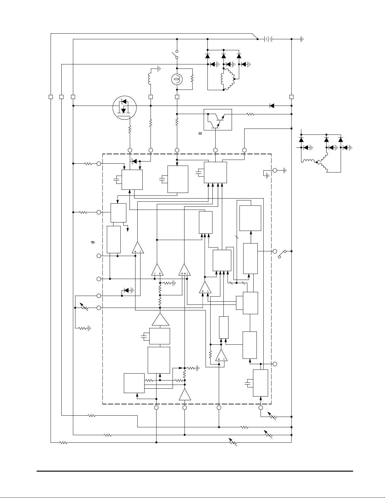
Figure 1. Simplified Application
28 k
R3
86 k
ref
V
UV
FB
45 k
20
19
1
28 k
MC33092
Lost
Sense
Circuit
Load Dump
Buff
Low
Pass
Filter
Signal
Combiner
and Switch
2
Sense
(Remote)
Overvoltage
Regulate
X1
12
Reg
(Local)
Supply
10
Logic
Control
12
Counter
Phase
4
DAC
R1
(1/12/48)
Divide By
)
8
(2
Counter
)
4
(2
Prescaler
Oscillator
7
12.5 k
2.5 sec
Oscillator 9
280kHz
R2
Osc.
10 sec
Adjust
RT
R3 = 10 k to 15 k
RT = 50 k to 100 k
NOTES: R1 = R2 = 3.0 k to 5.0 k
Figure 1.
MOTOROLA ANALOG IC DEVICE DATA
3

MC33092A
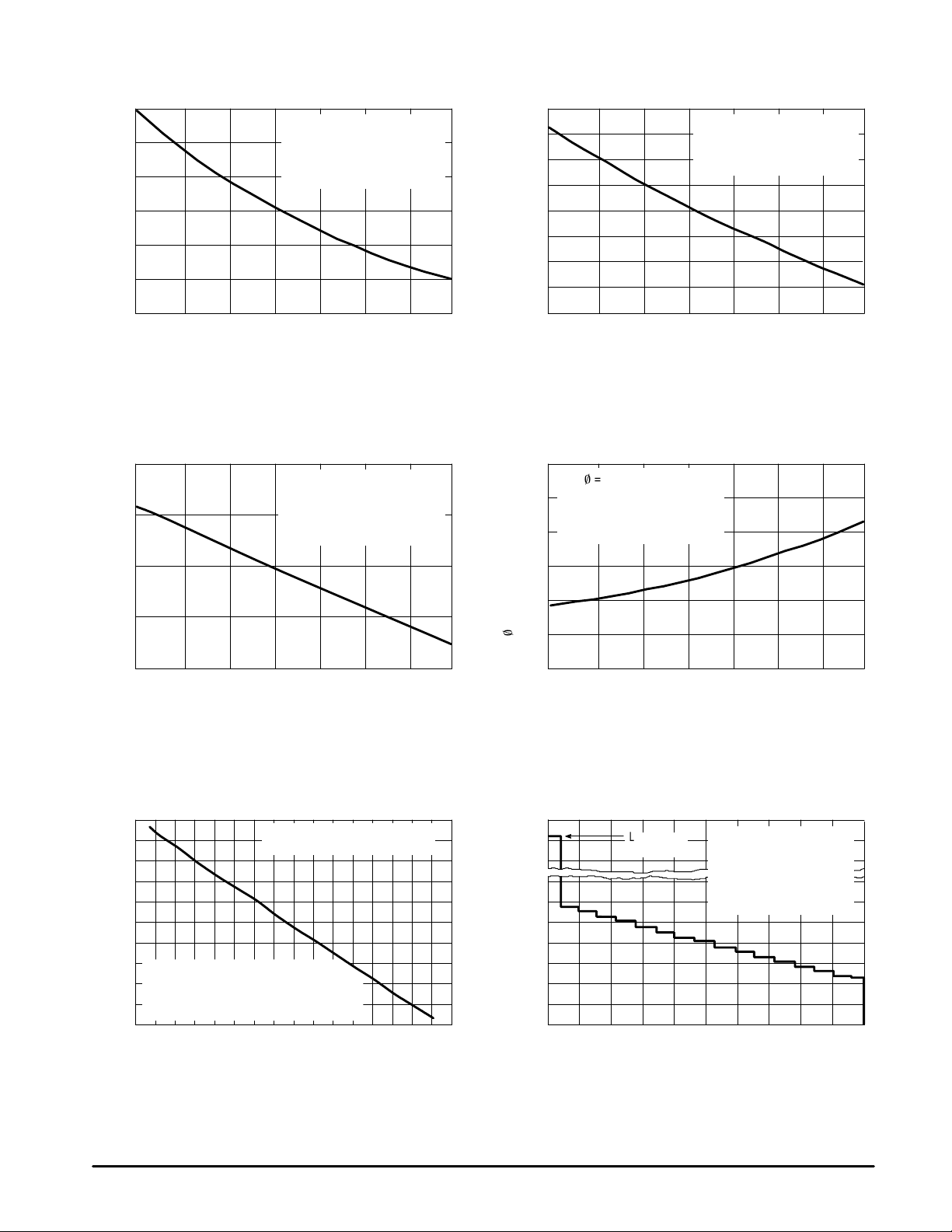
Figure 2. Standby Current versus T emperature Figure 3. T urn–On Voltage versus Temperature
0.8
0.7
0.6
0.5
0.4
, STANDBY CURRENT (mA)
SB
0.3
I
0.2
– 55 – 25 0 25 50 75 100 125
TA, AMBIENT TEMPERATURE (°C)
ISB = Current from VCC Supply
VCC = 12.8 V (see Figure 8)
VC1 = 0.5 V (Ignition OFF)
V
= V
= V
Pin 12
Pin 11
= 1.5 V
= V
Pin 19
Pin 2
V
Pin 10
Figure 4. Reference V oltage versus Temperature
2.2
V
= Voltage at Pin 20
ref
VCC = 12.8 V (see Figure 8)
2.1
VC1 = 0.5 V (Ignition OFF)
V
Pin 2
V
Pin 10
= V
= V
Pin 12
Pin 11
= 1.5 V
= V
Pin 19
= 0 V
= 0 V
1.8
1.7
1.6
1.5
1.4
1.3
, TURN-ON VOLTAGE (V)
1.2
On
1.1
1.0
– 55 – 25 0 25 50 75 100 125
TA, AMBIENT TEMPERATURE (°C)
VON = Voltage at Pin 3
VCC = 12.8 V (see Figure 8)
V
= V
Pin 2
Pin 10
= V
Pin 12
Pin 11
V
Figure 5. 0TC Reference V oltage
versus T emperature
1.26
V
O
= Voltage at Pin 8
ref
VCC = 12.8 V (see Figure 8)
1.25
VC2 = 6.0 V (S1 Closed)
V
1.24
Pin 2
V
Pin 10
= V
= V
Pin 12
Pin 11
= 1.5 V
= V
Pin 19
= 0 V
= 1.5 V
= V
Pin 19
= 0 V
2.0
1.9
, REFERENCE VOLTAGE (V)
ref
V
1.8
– 55 – 25 0 25 50 75 100 125
TA, AMBIENT TEMPERATURE (°C)
Figure 6. Oscillator Frequency
versus Timing Resistor
110
100
Ω
90
80
, RESISTANCE (k )
T
VCC = 14.8 V (see Figure 8)
R
VC2 = 6.0 V (S1 Closed)
70
V
= V
Pin 2
Pin 10
= 0 V
Pin 11
220 240 260 280 300 320 340 360 10 20 30 40 50 60 70 80 90 100
60
V
200
R = Resistance from Pin 7 to Ground
f = Frequency at Pin 9
= V
Pin 12 = VPin 19
f, FREQUENCY (kHz)
= 1.5 V
1.23
1.22
O
1.21
ref
V , 0TC REFERENCE VOLTAGE (V)V
1.20
– 55 – 25 0 25 50 75 100 125
°
TA, AMBIENT TEMPERATURE (
C)
Figure 7. Input V oltage versus Output Duty Cycle
3.0
Vin = Voltage at Pin 2 or 12
Duty Cycle taken at Pin 17
VCC = 14.8 V (see Figure 8)
VC2 = 6.0 V (S1 Closed)
V
= 1.5 V @ > 309 Hz
Pin 10
V
Pin 11
= 0 V; V
Pin 19
= 1.5 V
, INPUT VOLTAGE (V) V
Input
2.5
2.0
1.96
1.95
1.94
1.93
Load Dump
Protection
0
DC, DUTY CYCLE (%)
4
MOTOROLA ANALOG IC DEVICE DATA
 Loading...