Device
Operating
Temperature Range
Package
SEMICONDUCTOR
TECHNICAL DATA
HIGH–SIDE
TMOS DRIVER
ORDERING INFORMATION
MC33091AD
MC33091AP
TA = – 40° to +125°C
SO–8
Plastic DIP
PIN CONNECTIONS
Order this document by MC33091A/D
D SUFFIX
PLASTIC PACKAGE
CASE 751
(SO–8)
8
1
8
1
P SUFFIX
PLASTIC PACKAGE
CASE 626
1
SRC
Gnd
V
T
Input
Fault
V
CC
2
3
4
8
7
6
5
DRN
Gate
(Top View)
1
MOTOROLA ANALOG IC DEVICE DATA
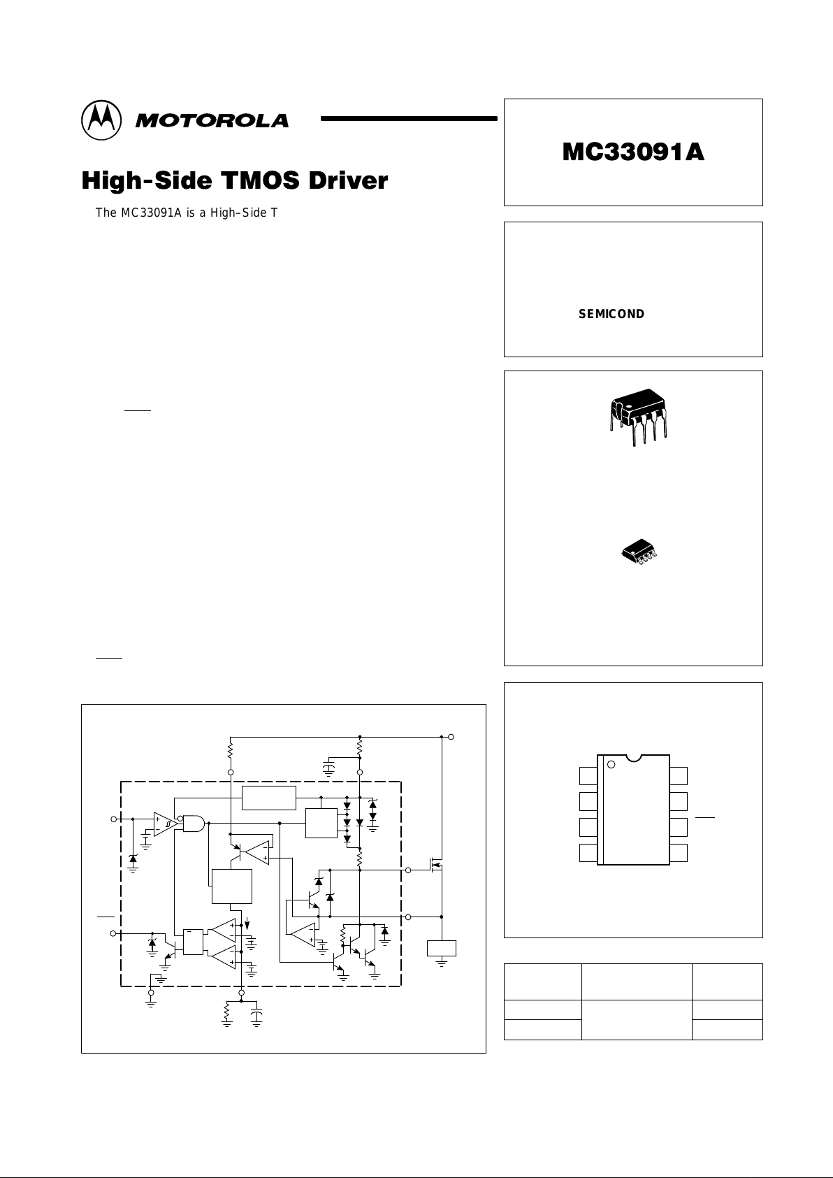
The MC33091A is a High–Side TMOS Driver designed for use in harsh
automotive switching applications requiring the capability of handling high
voltages attributed to load and field dump transients, as well as reverse and
double battery conditions. Few external components are required to drive a
wide variety of N–Channel TMOS devices. The MC33091A, driving an
appropriate TMOS device, offers economical system solutions for high–side
switching large currents. The MC33091A has CMOS compatible input
control, charge pump to drive the TMOS power transistor, basic fault
detection circuit, VDS monitoring circuit used to detect a shorted TMOS load,
and overcurrent protection timer with associated current squaring circuitry.
Short circuit protection is made possible by having a unique VDS voltage
to current converter drive an externally programmable integrator circuit. This
circuit affords fast detection of a shorted load while allowing difficult loads,
such as lamps having high in–rush currents, additional time to turn on.
The Fault
output is comprised of an open collector NPN transistor
requiring a single pull–up resistor for operation. A fault is reported whenever
the MOSFET on–current exceeds an externally programmed set level.
The MC33091A is available in the plastic 8–Pin DIP package as well as
the plastic 8–Pin surface mount package.
• Designed for Automotive High–Side Driver Applications
• Works with a Wide Variety of N–Channel Power MOSFETs
• Drives Inductive Loads with No External Clamp Circuitry Required
• CMOS Logic Compatible Input Control
• On–Board Charge Pump with No External Components Required
• Shorted Load Detection and Protection
• Forward Overvoltage and Reverse Battery Protection
• Load and Field Dump Protection
• Extended Operating Temperature Range
• Fault Output to Report a MOSFET Overcurrent Condition
SQ
+
+
I
SQ
Fault
Overvoltage
Shutdown
R
X
R
S
DRN2
C
S
VCC5
+V
S
Input
7
6
+
QR
Current
Squaring
Circuit
+
Gnd3V
T
8
C
T
R
T
Charge
Pump
Gate
4
SRC
1
Load
MC33091A
Simplified Block Diagram
This device contains 54 active transistors.
Motorola, Inc. 1996 Rev 0

MC33091A
2
MOTOROLA ANALOG IC DEVICE DATA
MAXIMUM RATINGS
Rating Symbol Value Unit
Supply Voltage (Pin 5) (Note 1) V
CC
–0.7 to 28 V
Continuous (Without Activating Clamp) 7.0 to 28
Continuous Supply Clamp Current (Pin 5) I
C
mA
DIP Package (Case 626) 10
SO–8 Package (Case 751) 1.0
Input Control Voltage Range (Pin 7) V
in
V
Continuous –0.7 to 28
Fault Pull–Up Voltage Range (Pin 6) V
out
V
Continuous –0.7 to 28
Minimum ESD Voltage Capability (Note 2) ESD 2000 V
Operating Junction Temperature T
J
150 °C
Storage Temperature T
stg
–65 to +150 °C
Operating Ambient Temperature Range T
A
–40 to +125 °C
Thermal Resistance, Junction–to–Ambient R
θJA
°C/W
DIP Package (Case 626) 100
SO–8 Package (Case 751) 145
NOTES: 1. An internal zener diode is incorporated to protect the device from overvoltage transients in excess
of 30 V.
2.ESD testing performed in accordance with Human Body Model (C = 100 pF, R = 1500 Ω).
SQ
+
+
I
SQ
Fault
Overvoltage
Shutdown
RX = 75 k
RS = 200
DRN2
0.1
V
CC
5
+V
S
Input
7
6
+
QR
Current
Squaring
Circuit
+
Gnd3V
T
8
C
T
R
T
Charge
Pump
Gate
4
SRC
1
Load
MC33091A
9.1 k
2.6 V
40 V
40 V
V
TH
4.3 V
V
TL
0.95 V
14 V
1.0 V
R
30 V
1.0 k
Figure 1. Typical Application
+5.0 V

MC33091A
3
MOTOROLA ANALOG IC DEVICE DATA
ELECTRICAL CHARACTERISTICS (Values are noted under conditions of 7.0 V ≤ V
CC
≤ 24 V, –40°C ≤ TA ≤ +125°C, unless otherwise
noted. Typical values reflect approximate mean at TA = 25°C at time of device characterization.)
Characteristics Symbol Min Typ Max Unit
Supply Current (Note 1) I
CC
Vin = 0 V – 160 300 µA
Vin = 5.0 V (RX = 100 k) – 2.5 6.0 mA
Supply Clamp Voltage (Note 2) V
Z
29 – 35 V
Gate–to–Source Voltage Range (Pin 4) V
GS
8.0 12 15 V
Gate Current (Pin 4) I
G
µA
VG = V
CC
30 – 400
Gate Saturation Voltage (IG = 10 µA) V
G(sat)
0 1.2 1.4 V
Short Circuit Gate Voltage (Note 4) I
GC
6.4 7.0 7.7 V
Input Control Threshold Voltage (Pin 7) V
V
IL
– 2.7 1.5
V
IH
3.5 2.7 –
Input Control Current (Pin 7) (Vin = 5.0 V) I
in
– 100 250 µA
Timer Current Constant (Pin 8) K µA/V
2
(RX = 100 k, VT = 0, VDS = 1.0 V) (Note 3) 0.7 1.1 1.5
Timer (Pin 8) V
Lower Threshold Voltage V
TL
0.4 0.95 1.2
Upper Threshold Voltage V
TH
4.3 4.6 5.2
Fault Sink Current (Pin 6)
VF = 5.0 V I
OL
500 – – µA
VF = 0 I
OH
– 2.0 100 nA
Fault Saturation Voltage (Pin 6) (IF = 500 µA) V
OL
– 0.2 0.8 V
NOTES: 1. The total supply current into Pin 2 and Pin 5 with RX = 100 k (from Pin 2 to supply) and 45 k pull–up resistor from Pin 6 to supply.
2.An internal zener clamp is provided to protect the device from overvoltage transients on the supply line.
3.The timer current constant is the proportionality constant of the voltage to current converter used to monitor the VDS voltage developed across the
FET (from Pin 1 to the supply).
4.The gate voltage will be clamped at approximately 7.0 V above the source voltage whenever the source voltage is less than approximately 1.0 V
above ground.
I
CC
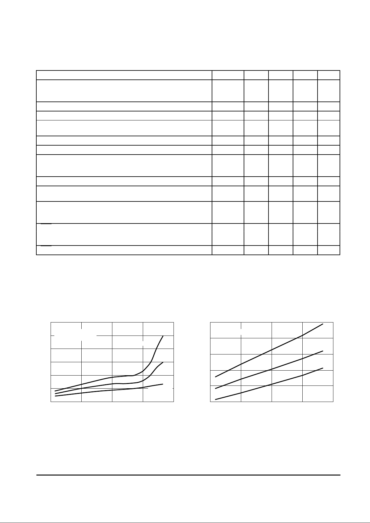
Figure 2. Supply Current versus Supply Voltage
600
500
400
300
200
100
0
, SUPPLY CURRENT ( A)
Figure 3. Operating Current versus Supply Voltage
6.0
2.0
1.0
I
CC
TA = –40°C
TA = 25°C
TA = 125°C
Vin = 0 V (Gate “off”)
VDS = 2.0 V
5.0
4.0
3.0
, OPERATING CURRENT (mA)
VCC, SUPPLY VOLTAGE (V)
6.0 12 18 24 30
VCC, SUPPLY VOLTAGE (V)
6.0 12 18 24 30
TA = –40°C
TA = 25°C
TA = 125°C
Vin = 5.0 V (Gate “on”)
µ

MC33091A
4
MOTOROLA ANALOG IC DEVICE DATA
600
0.1
500
400
100
0.1
350
, TIMER CURRENT (I
SQ
250
200
150
100
50
µ
VCC = 14 V
Vin = 5.0 V
RX = 75 k
300
200
VCC = 14 V
Vin = 5.0 V
TA = 25
°
C
RX = 50 k
RX = 100 k
RX = 75 k
V
DS
2
, DRAIN–TO–SOURCE VOL TAGE SQUARED (V2)
0 50 100 150 200
V
DS
2
, DRAIN–TO–SOURCE VOL TAGE SQUARED (V2)
0.1 50 100 150 200
A)
200
0
180
160
140
100
80
60
120
, INPUT CONTROL CURRENT (I
in
100
80
60
40
20
µ
VCC = 14 V
TA = 25
°
C
120
Vin = 5.0 V
TA = 125°C
TA = 25°C
TA = –40°C
Vin, INPUT CONTROL VOLTAGE (V)
6.0 12 18 24 30
VCC, SUPPLY VOLTAGE (V)
0 1.0 2.0 3.0 4.0 5.0 6.0
A)
1.30
, CURRENT SQUARING CONSTANT ( A/V )K
0
1.25
1.20
1.05
1.00
0.95
1.4
, FAULT VOLTAGE (V)V
Fault
1.0
0.8
0.6
0.4
0.2
VCC = 14 V
TA = 25
°
C
µ
2
1.15
1.10
RX = 100 k
VDS = 2.0 V
TA = 125°C
TA = 25°C
TA = –40°C
I
Fault
, FAULT
SINK CURRENT (mA)
6.0 12 18 24 30
VCC, SUPPLY VOLTAGE (V)
0 1.0 2.0 3.0 4.0 5.0
160
140
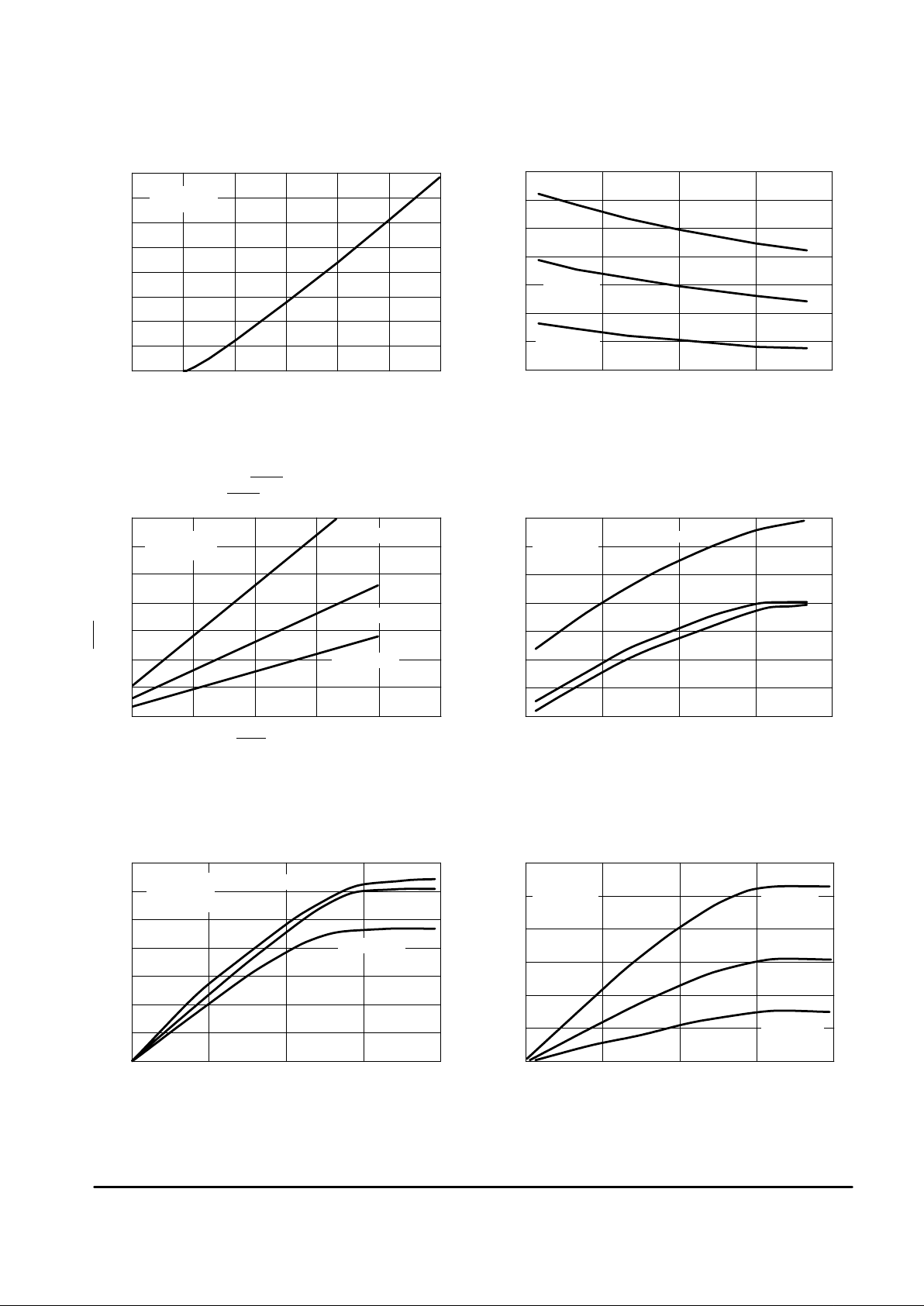
Figure 4. Input Control Current
versus Input Control Voltage
Figure 5. Input Control Current
versus Supply Voltage
Figure 6. Fault
Voltage versus
Fault
Sink Current
Figure 7. Squaring Constant “K”
versus Supply Voltage
Figure 8. Timer Current versus
Drain–to–Source Voltage Squared
Figure 9. Timer Current versus
Drain–to–Source Voltage Squared
, INPUT CONTROL CURRENT (I
in
µ
A)
TA = –40°C
TA = 25°C
TA = 125°C
TA = 125°C
TA = 25°C
TA = –40°C
300
, TIMER CURRENT (I
SQ
µ
A)
1.2

MC33091A
5
MOTOROLA ANALOG IC DEVICE DATA
, TIMER LOWER THRESHOLD VOLTAGE (V)V
TL
, TIMER LOWER THRESHOLD VOLTAGE (V)V
TL
, TIMER UPPER THRESHOLD VOL TAGE (V)V
TH
TA, AMBIENT TEMPERATUE (°C)
45
4.52
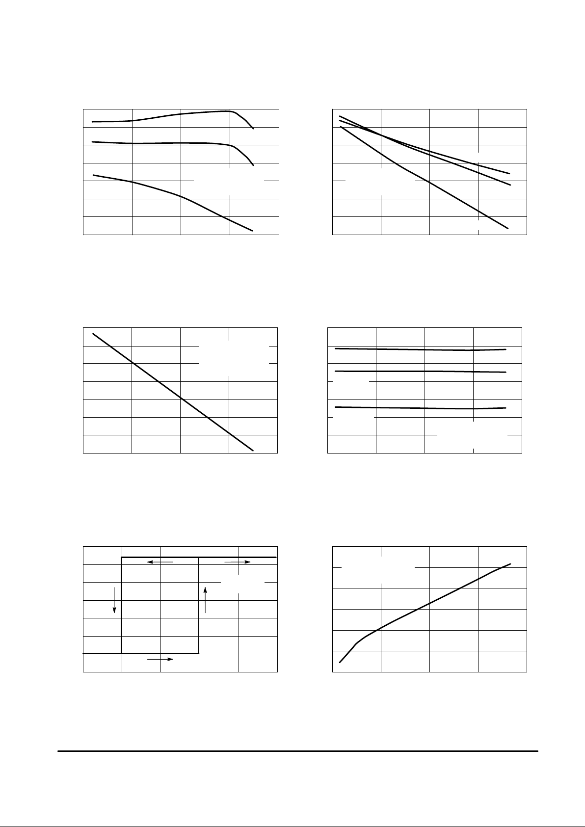
Figure 10. Timer Upper Threshold Voltage
versus Temperature
4.64
4.62
4.60
4.58
4.56
4.54
4.50
Figure 11. Timer Upper Threshold Voltage
versus Supply Voltage
4.64
4.62
4.60
4.58
4.50
Figure 12. Timer Lower Threshold Voltage
versus Temperature
1.10
1.05
1.00
0.95
0.85
0.80
0.75
Figure 13. Timer Lower Threshold Voltage
versus Supply Voltage
1.2
1.1
1.0
0.9
0.8
0.5
Figure 14. Gate Voltage versus
Input Control Voltage
–5.0
Figure 15. Gate Voltage versus
Supply Voltage
40
35
20
15
30
, TIMER UPPER THRESHOLD VOL TAGE (V)V
TH
4.52
4.56
4.54
0.7
0.6
, GATE VOLTAGE (V)V
G
25
20
15
10
5.0
30
25
–50 0 50 150
6.0
VCC, SUPPLY VOLTAGE (V)
12 18 24
–50 0 50 100 150
TA, AMBIENT TEMPERATUE (
°
C)
6.0 12 18 24 30
VCC, SUPPLY VOLTAGE (V)
Vin, INPUT CONTROL VOLTAGE (V)
6.0 12 18 24 30
VCC, SUPPLY VOLTAGE (V)
2.0 2.2 2.4 2.6 2.8 3.0
30
100
, GATE VOLTAGE (V)V
G
Vin = 5.0 V
VTH = Increasing V
T
causing Gate turn–off
VCC = 7.0 V
VCC = 14 V
VCC = 28 V
TA = –40°C
TA = 125°C
TA = 25°C
Vin = 5.0 V
VTH = Increasing V
T
causing Gate turn–off
0.90
7.0 V ≤ VCC ≤ 28 V
Vin = 5.0 V
VTL = Decreasing V
T
causing Gate turn–on
TA = –40°C
TA = 25°C
TA = 125°C
Vin = 5.0 V
VTL = Decreasing V
T
causing Gate turn–on
VCC = 14 V
TA = 25
°
C
–40°C ≤ TA ≤ 125°C
Vin = 5.0 V (Gate “on”)
IG
≤
5.0 µA
0
 Loading...