

Order this document by MC34067/D
The MC34067/MC33067 are high performance zero voltage switch
resonant mode controllers designed for off–line and dc–to–dc converter
applications that utilize frequency modulated constant off–time or constant
deadtime control. These integrated circuits feature a variable frequency
oscillator, a precise retriggerable one–shot timer, temperature compensated
reference, high gain wide bandwidth error amplifier, steering flip–flop, and
dual high current totem pole outputs ideally suited for driving power
MOSFETs.
Also included are protective features consisting of a high speed fault
comparator, programmable soft–start circuitry, input undervoltage lockout
with selectable thresholds, and reference undervoltage lockout.
These devices are available in dual–in–line and surface mount packages.
• Zero Voltage Switch Resonant Mode Operation
• Variable Frequency Oscillator with a Control Range Exceeding 1000:1
• Precision One–Shot Timer for Controlled Of f–Time
• Internally Trimmed Bandgap Reference
• 4.0 MHz Error Amplifier
• Dual High Current Totem Pole Outputs
• Selectable Undervoltage Lockout Thresholds with Hysteresis
• Enable Input
• Programmable Soft–Start Circuitry
• Low Startup Current for Off–Line Operation
HIGH PERFORMANCE
ZERO VOLTAGE SWITCH
RESONANT MODE
CONTROLLERS
SEMICONDUCTOR
TECHNICAL DATA
P SUFFIX
PLASTIC PACKAGE
CASE 648
DW SUFFIX
PLASTIC PACKAGE
CASE 751G
(SO–16L)
16
1
16
1
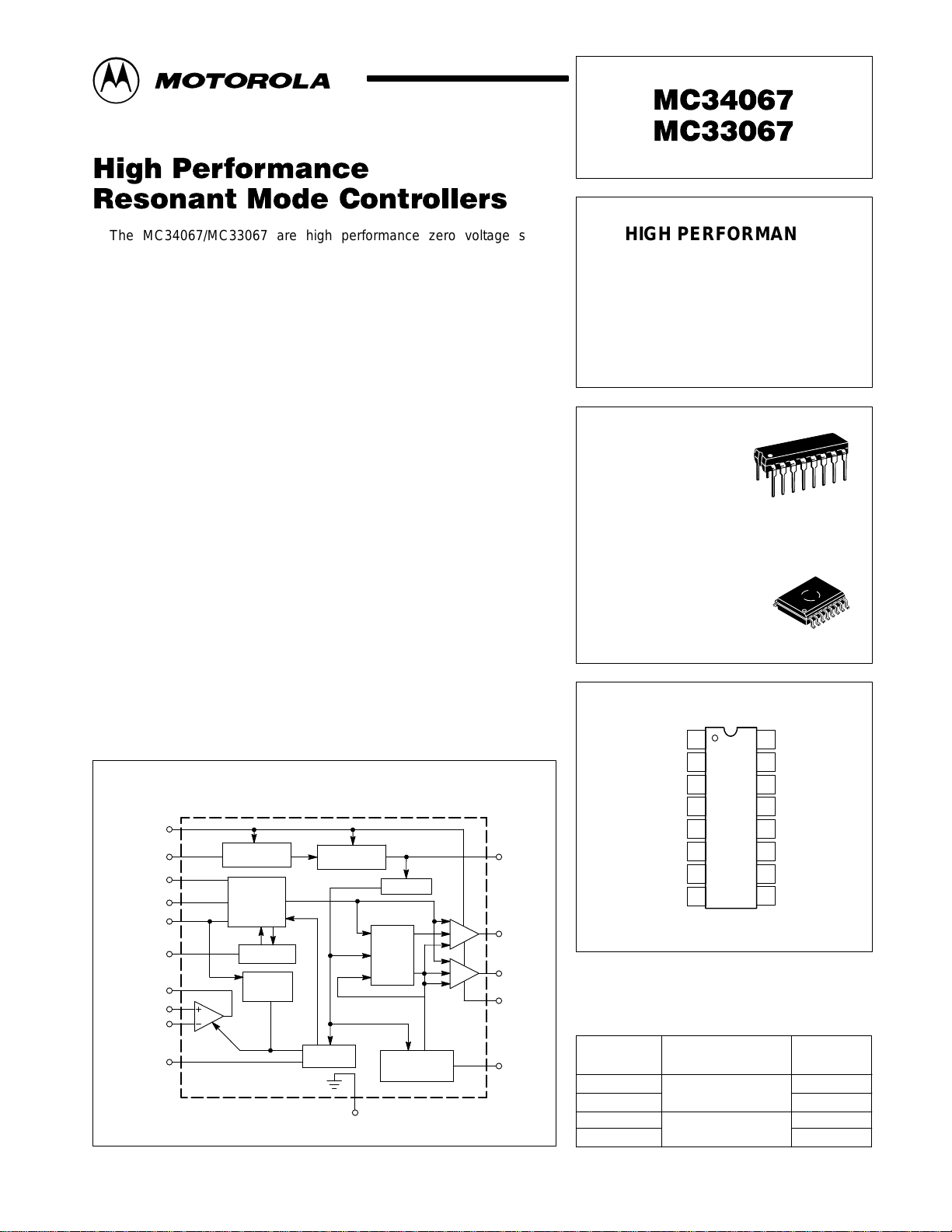
Simplified Block Diagram
15
V
CC
Enable /
UVLO Adjust
Osc Charge
Osc RC
Oscillator
Control Current
One–Shot
Error Amp
Output
Noninverting
Input
Inverting Input
Soft–Start
9
1
2
3
16
6
8
7
11
Error
Amp
V
UVLO /
CC
Enable
Variable
Frequency
Oscillator
One–Shot
2.5 V
Clamp
5.0 V
Reference
Soft–Start
MOTOROLA ANALOG IC DEVICE DATA
V
Steering
Flip–Flop
Fault Detector
Ground4
UVLO
ref
5
V
ref
14
Output A
12
Output B
13
Pwr Gnd
10
Fault Input
PIN CONNECTIONS
Osc Charge
Osc RC
Osc Control Current
Gnd
V
ref
Error Amp Out
Inverting Input
Noninverting Input
1
2
3
4
5
6
7
8
(Top View)
One–Shot RC
16
V
15
CC
Drive Output A
14
Power Gnd
13
Drive Output B
12
C
11
Soft–Start
Fault Input
10
Enable/UVLO
9
Adjust
ORDERING INFORMATION
Operating
Device
MC34067DW SO–16L
MC34067P Plastic DIP
MC33067DW SO–16L
MC33067P Plastic DIP
Motorola, Inc. 1999 Rev 1, 05/99
Temperature Range
TA = 0 to + 70°C
TA = – 40° to + 85°C
Package
1
MC34067 MC33067
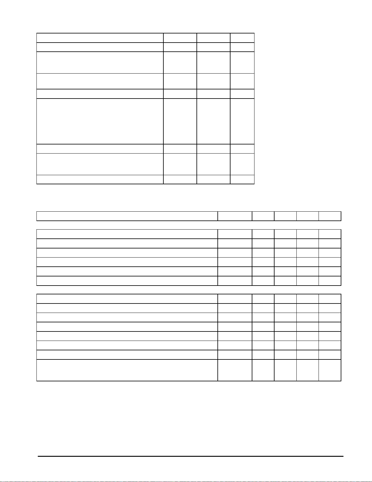
MAXIMUM RATINGS
Rating Symbol Value Unit
Power Supply Voltage V
Drive Output Current, Source or Sink (Note 1)
Continuous
Pulsed (0.5 µs, 25% Duty Cycle
Error Amplifier, Fault, One–Shot, Oscillator and
Soft–Start Inputs
UVLO Adjust Input V
Power Dissipation and Thermal Characteristics
DW Suffix, Plastic Package, Case 751G
TA = 25°C
Thermal Resistance, Junction–to–Air
P Suffix, Plastic Package, Case 648
TA = 25°C
Thermal Resistance, Junction–to–Air
Operating Junction Temperature T
Operating Ambient Temperature
MC34067
MC33067
Storage Temperature T
CC
I
O
V
in
in(UVLO)
P
D
R
θJA
P
D
R
θJA
J
T
A
stg
20 V
0.3
1.5
– 1.0 to + 6.0 V
– 1.0 to V
862
145
1.25
100
CC
mW
°C/W
W
°C/W
+ 150 °C
°C
0 to + 70
– 40 to + 85
– 55 to + 150 °C
A
V
ELECTRICAL CHARACTERISTICS (V
= 12 V [Note 2], R
CC
OSC
= 18.2 k, R
VFO
= 2940, C
= 300 pF, RT = 2370 k, CT = 300 pF,
OSC
CL = 1.0 nF. For typical values TA = 25°C, for min/max values TA is the operating ambient temperature range that applies [Note 3], unless
otherwise noted.)
Characteristic
Symbol Min Typ Max Unit
REFERENCE SECTION
Reference Output Voltage (IO = 0 mA, TJ = 25°C) V
Line Regulation (VCC = 10 TO 18 V) Reg
Load Regulation (IO = 0 mA to 10 mA) Reg
Total Output Variation Over Line, Load, and Temperature V
Output Short Circuit Current I
Reference Undervoltage Lockout Threshold V
ref
line
load
ref
O
th
5.0 5.1 5.2 V
– 1.0 20 mV
– 1.0 20 mV
4.9 – 5.3 V
25 100 190 mA
3.8 4.3 4.8 V
ERROR AMPLIFIER
Input Offset Voltage (VCM = 1.5 V) V
Input Bias Current (VCM = 1.5 V) I
Input Offset Current (VCM = 1.5 V) I
Open Loop Voltage Gain (VCM = 1.5 V, VO = 2.0 V) A
IO
IB
IO
VOL
– 1.0 10 mV
– 0.2 1.0 µA
– 0 0.5 µA
70 100 – dB
Gain Bandwidth Product (f = 100 kHz) GBW 3.0 5.0 – MHz
Input Common Mode Rejection Ratio (VCM = 1.5 to 5.0 V) CMR 70 95 – dB
Power Supply Rejection Ratio (VCC = 10 to 18 V, f = 120 Hz) PSR 80 100 – dB
Output Voltage Swing
High State
Low State
NOTES: 1. Maximum package power dissipation limits must be observed.
2.Adjust VCC above the Startup threshold before setting to 12 V.
3.Low duty cycle pulse techniques are used during test to maintain junction temperature as close to ambient as possible.
T
=0°C for the MC34067 T
low
=–40°C for the MC33067 T
= + 70°C for MC34067
high
= + 85°C for MC33067
high
V
OH
V
OL
2.8
–
3.2
0.6
–
0.8
V
2
MOTOROLA ANALOG IC DEVICE DATA
MC34067 MC33067
ELECTRICAL CHARACTERISTICS (V
= 12 V [Note 2], R
CC
OSC
= 18.2 k, R
VFO
= 2940, C
= 300 pF, RT = 2370 k, CT = 300 pF,
OSC
CL = 1.0 nF. For typical values TA = 25°C, for min/max values TA is the operating ambient temperature range that applies [Note 3], unless
otherwise noted.)
Characteristic
Symbol Min Typ Max Unit
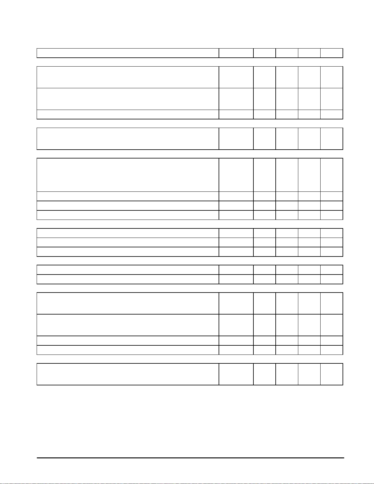
OSCILLAT OR
Frequency (Error Amp Output Low)
TA = 25°C
Total Variation (VCC = 10 to 18 V, TA = T
Low
to T
High
f
OSC(low)
Frequency (Error Amp Output High)
TA = 25°C
Total Variation (VCC = 10 to 18 V, TA = T
Low
to T
High
f
OSC(high)
Oscillator Control Input Voltage, Pin 3 @ 25°C V
500
490
1900
1850
in
– 2.5 – V
525
–
540
550
2050–2150
2200
kHz
kHz
ONE–SHOT
Drive Output Off–Time
TA = 25°C
Total Variation (VCC = 10 to 18 V, TA = T
Low
to T
High
t
Blank
235
225
250
–
270
280
ns
DRIVE OUTPUTS
Output Voltage
Low State (I
Low State (I
High State (I
High State (I
Output Voltage with UVLO Activated (VCC = 6.0 V, I
= 20 mA)
Sink
= 200 mA)
Sink
Source
Source
= 20 mA)
= 200 mA)
= 1.0 mA) V
Sink
V
V
OL(UVLO)
Output Voltage Rise T ime (CL = 1.0 nF) t
Output Voltage Fall T ime (CL = 1.0 nF) t
OL
OH
r
f
–
–
9.5
9.0
0.8
1.5
10.3
9.7
1.2
2.0
–
–
– 0.8 1.2 V
– 20 50 ns
– 15 50 ns
V
FAULT COMP ARATOR
Input Threshold V
Input Bias Current (V
Propagation Delay to Drive Outputs (100 mV Overdrive) t
= 0 V) I
Pin 10
PLH(In/Out)
th
IB
0.93 1.0 1.07 V
– –2.0 –10 µA
– 60 100 ns
SOFT–START
Capacitor Charge Current (V
Capacitor Discharge Current (V
= 2.5 V) I
Pin 11
= 2.5 V) I
Pin 11
chg
dischg
4.5 9.0 14 µA
3.0 8.0 – mA
UNDERVOLTAGE LOCKOUT
Startup Threshold, VCC Increasing
Enable/UVLO Adjust Pin Open
Enable/UVLO Adjust Pin Connected to V
CC
Minimum Operating Voltage After Turn–On
Enable/UVLO Adjust Pin Open
Enable/UVLO Adjust Pin Connected to V
CC
Enable/UVLO Adjust Shutdown Threshold Voltage V
Enable/UVLO Adjust Input Current (Pin 9 = 0 V) I
V
th(UVLO)
V
CC(min)
th(Enable)
in(Enable)
14.8
8.0
8.0
7.6
16
9.0
9.0
8.6
17.2
10
10
9.6
6.0 7.0 – V
– –0.2 –1.0 mA
V
V
TOTAL DEVICE
Power Supply Current (Enable/UVLO Adjust Pin Open)
Startup (VCC = 13.5 V)
Operating (f
NOTES: 1. Maximum package power dissipation limits must be observed.
2.Adjust VCC above the Startup threshold before setting to 12 V.
3.Low duty cycle pulse techniques are used during test to maintain junction temperature as close to ambient as possible.
T
low
= 500 kHz) (Note 2)
OSC
=0°C for the MC34067 T
=–40°C for the MC33067 T
= + 70°C for MC34067
high
= + 85°C for MC33067
high
I
CC
–
–
0.5
27
0.8
35
mA
MOTOROLA ANALOG IC DEVICE DATA
3
MC34067 MC33067
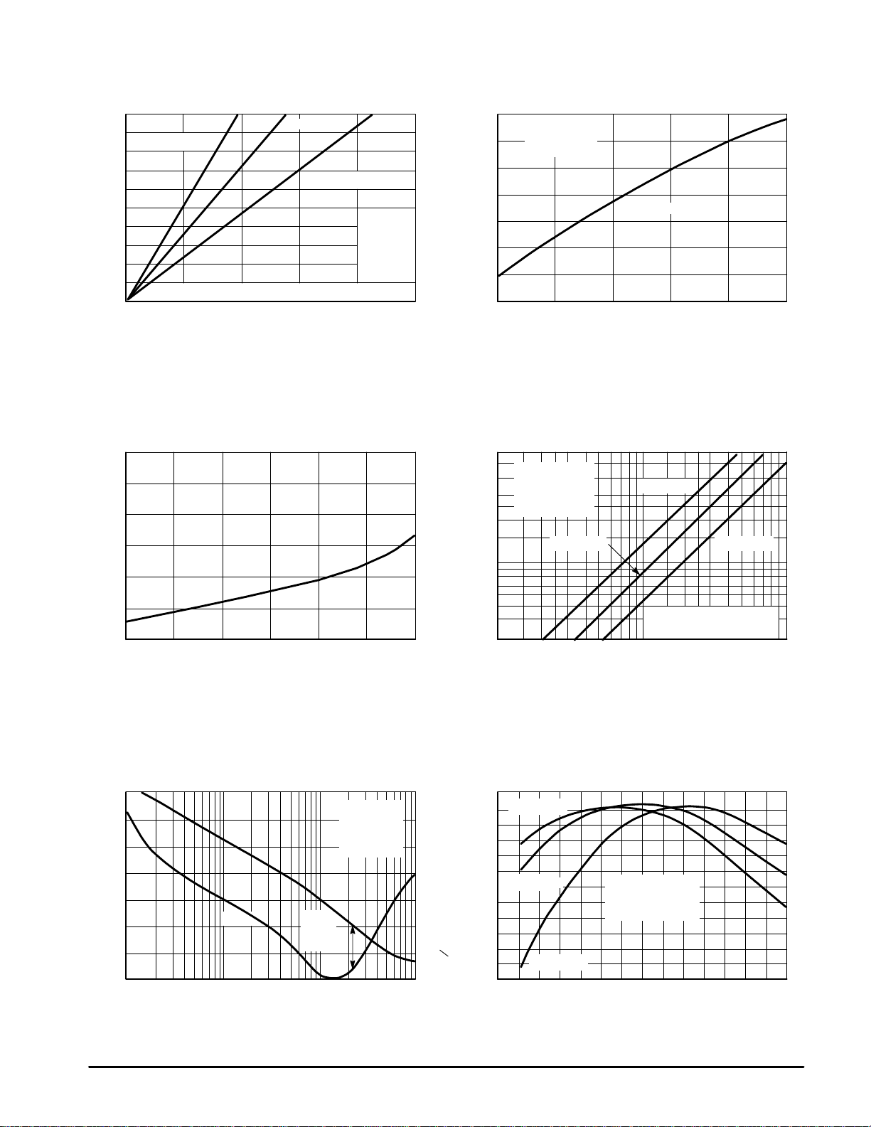
Figure 1. Oscillator Timing Resistor
versus Discharge Time
500
Ω
400
300
200
100
, OSCILLAT OR TIMING RESIST OR (k )
OSC
R
C
= 300 pF
OSC
C
= 200 pF
OSC
C
= 500 pF
OSC
VCC = 12 V
∞
R
=
VFO
RT =
∞
CT = 500 pF
°
C
TA = 25
0
Oscillator Discharge Time is Measured at the Drive Outputs.
t
, OSCILLAT OR DISCHARGE TIME (µs)
dischg
3500
3000
2500
2000
1500
1000
, OSCILLAT OR FREQUENCY (kHz)
500
OSC
f
Figure 3. Error Amp Output Saturation
V oltage versus Oscillator Control Current
0.35
0.30
0.25
0.20
0.15
0.10
, OUTPUT SA TURATION VOLTAGE (V)
sat
V
0.05
0 0.5 1.0 1.5 2.0 2.5 3.0 0.1 0.3 0.6 1.0 3.0 6.0 10
I
, OSCILLAT OR CONTROL CURRENT (mA) tOS, ONE–SHOT PERIOD (
OSC
60
30
Ω
20
10
, TIMING RESISTOR (k )
400
T
R
3.0
Figure 2. Oscillator Frequency versus
Oscillator Control Current
VCC = 12 V
°
C
TA = 25
R
= 18.2 k
OSC
C
= 300 pF
OSC
0
0 400 800 1200 1600 20000 20406080100
I
, OSCILLAT OR CONTROL CURRENT (mA)
OSC
Figure 4. One–Shot Timing Resistor
versus Period
VCC = 12 V
C
= 500 pF
OSC
R
= 100 k
OSC
°
C
TA = 25
CT = 300 pF CT = 500 pF
CT = 200 pF
One–Shot Period is Measured
at the Drive Outputs.
µ
s)
Figure 5. Open Loop V oltage Gain and Phase
versus Frequency
50
Phase
Margin
°
= 64
VCC = 12 V
VO = 2.0 V
RL = 100 k
TA = 25
40
30
20
10
0
, OPEN LOOP VOL TAGE GAIN (dB)
–10
VOL
A
–20
10 k 100 k 1.0M 10M – 55 – 25 0 25 50 75 125100
Gain
Phase
f, FREQUENCY (Hz)
50
60
70
°
C
80
90
100
0, EXCESS PHASE (DEGREES)
110
120
, REFERENCE OUTPUT VOLTAGE CHANGE (mV)
∇
V
4
Figure 6. Reference Output V oltage Change
versus T emperature
*V
= 5.0 V
ref
0
–10
–20
*V
= 5.0 V
–30
–40
–50
ref
ref
*V
= 5.0 V
ref
TA, AMBIENT TEMPERATURE (°C)
VCC = 12 V
∞
RL =
*V
ref at TA
= 25°C
MOTOROLA ANALOG IC DEVICE DATA
MC34067 MC33067
Figure 7. Reference V oltage Change
0
–10
–20
–30
–40
–50
, REFERENCE OUTPUT VOLTAGE CHANGE (mV)
ref
V
∇
VCC = 12 V
Figure 9. Drive Output Waveform
90%
versus Source Current
TA = – 40°C
TA = – 20°C
TA = –125°C
I
, REFERENCE SOURCE CURRENT (mA)
ref
CL = 1.0 nF
TA = 25
Figure 8. Drive Output Saturation Voltage
versus Load Current
, OUTPUT SA TURATION VOLTAGE (V)
V
sat
–1.0
– 2.0
– 3.0
3.0
2.0
1.0
0
V
CC
TA = 25°C
TA = – 40°C
0
0 0.2 0.4 0.6 0.8 1.00 20 40 60 80 100
Source Saturation
(Load to Ground)
TA = – 40°C
TA = 25°C
Source Saturation
(Load to VCC)
IO, OUTPUT LOAD CURRENT (A)
80
VCC = 12 V
µ
s Pulsed Load
120 Hz Rate
Gnd
Figure 10. Soft–Start Saturation Voltage
versus Capacitor Discharge Current
3.2
°
C
2.4
10%
2000
1600
1200
800
f, FREQUENCY (kHz)
400
20 ns/DIV
Figure 11. Operating Frequency
versus Supply Current
VCC = 12 V
CL = 1.0 nF
°
C
TA = 25
1.6
0.8
OL
0
V , SOFT–START SATURATION VOLTAGE (V)
0 2.0 4.0 6.0 8.0 10
I
, CAPACITOR DISCHARGE CURRENT (mA)
dchg
VCC = 12 V
Pin 10 = V
TA = 25 °C
Figure 12. Supply Current versus Supply V oltage
24
TA = 25 °C
20
Enable/UVLO
Adjust Pin
Open
CC
I , SUPPLY CURRENT (mA)
16
12
8.0
4.0
Enable/UVLO
Adjust Pin
to V
CC
ref
0
30 40 50 60 70 80 90 0 4.0 8.0 12 16 20
ICC, INPUT SUPPLY CURRENT (mA)
0
VCC, SUPPLY VOLTAGE (V)
MOTOROLA ANALOG IC DEVICE DATA
5

C
R
T
OSC
C
OSC
R
T
Error Amp Output
Noninverting Input
V
CC
Enable /
UVLO Adjust
OSC Charge
OSC RC
One–Shot RC
Oscillator
Control Current
I
OSO
Inverting Input
R
VFO
Soft–Start
15
16
11
9
1
2
3
6
8
7
7.0k
Error Amp
MC34067 MC33067
Figure 13. MC34067 Representative Block Diagram
50k 7.0k
V
50k
I
OSC
8.0V
Q1
One–Shot
3.1V
Error Amp
Clamp
9.0
µ
VCC UVLO
V
D1
Oscillator
4.9V/3.6V
4.9V/3.6V
A
5.1V
Reference
ref
Q2
V
ref
ref
UVLO
Steering
Flip–Flop
T
Q
Q
R
4.2/4.0V
Fault Comparator
1.0V
V
ref
5
Output A
14
Power Ground
13
Output B
12
Fault Input
10
C
OSC
One–Shot
Output A
Output B
5.1 V
3. 6 V
5.1 V
3.6 V
Timing Diagram
t
OS
Error Amp output high, minimum I
occurring at minimum input voltage, maximum load.
t
OS
OSC
current
t
OS
Ground4
t
OS
Error Amp output low, maximum I
occurring at maximum input voltage, minimum load.
t
OS
t
OS
OSC
current
6
MOTOROLA ANALOG IC DEVICE DATA

MC34067 MC33067
OPERA TING DESCRIPTION
Introduction
As power supply designers have strived to increase power
conversion efficiency and reduce passive component size,
high frequency resonant mode power converters have
emerged as attractive alternatives to conventional
pulse–width modulated control. When compared to
pulse–width modulated converters, resonant mode control
offers several benefits including lower switching losses,
higher efficiency, lower EMI emission, and smaller size. A
new integrated circuit has been developed to support this
trend in power supply design. The MC34067 Resonant Mode
Controller is a high performance bipolar IC dedicated to
variable frequency power control at frequencies exceeding
1.0 MHz. This integrated circuit provides the features and
performance specifically for zero voltage switching resonant
mode power supply applications.
The primary purpose of the control chip is to provide a
fixed off–time to the gates of external power MOSFETs at a
repetition rate regulated by a feedback control loop.
Additional features of the IC ensure that system startup and
fault conditions are administered in a safe, controlled manner.
A simplified block diagram of the IC is shown on the front
page, which identifies the main functional blocks and the
block–to–block interconnects. Figure 13 is a detailed
functional diagram which accurately represents the internal
circuitry. The various functions can be divided into two
sections. The first section includes the primary control path
which produces precise output pulses at the desired
frequency. Included in this section are a variable frequency
Oscillator, a One–Shot, a pulse Steering Flip–Flop, a pair of
power MOSFET Drivers, and a wide bandwidth Error
Amplifier. The second section provides several peripheral
support functions including a voltage reference, undervoltage
lockout, Soft–Start circuit, and a fault detector.
Primary Control Path
The output pulse width and repetition rate are regulated
through the interaction of the variable frequency Oscillator,
One–Shot timer and Error Amplifier. The Oscillator triggers
the One–Shot which generates a pulse that is alternately
steered to a pair of totem pole output drivers by a toggle
Flip–Flop. The Error Amplifier monitors the output of the
regulator and modulates the frequency of the Oscillator. High
speed Schottky logic is used throughout the primary
control channel to minimize delays and enhance high
frequency characteristics.
Oscillator
The characteristics of the variable frequency Oscillator are
crucial for precise controller performance at high operating
frequencies. In addition to triggering the One–Shot timer and
initiating the output deadtime, the oscillator also determines
the initial voltage for the one–shot capacitor. The Oscillator is
designed to operate at frequencies exceeding 1.0 MHz. The
Error Amplifier can control the oscillator frequency over a
1000:1 frequency range, and both the minimum and
maximum frequencies are easily and accurately
programmed by the proper selection of external components.
The functional diagram of the Oscillator and One–Shot
timer is shown in Figure 14. The oscillator capacitor (C
initially charged by transistor Q1. When C
exceeds the
OSC
OSC
) is
4.9 V upper threshold of the oscillator comparator, the base
of Q1 is pulled low allowing C
external resistor, (R
(I
). When the voltage on C
OSC
and the oscillator control current,
OSC),
to discharge through the
OSC
falls below the
OSC
comparator’s 3.6 V lower threshold, Q1 turns on and again
charges C
C
OSC
high slew rate of C
.
OSC
charges from 3.6 V to 5.1 V in less than 50 ns. The
and the propagation delay of the
OSC
comparator make it difficult to control the peak voltage. This
accuracy issue is overcome by clamping the base of Q1
through a diode to a voltage reference. The peak voltage of
the oscillator waveform is thereby precisely set at 5.1 V.
Figure 14. Oscillator and One–Shot Timer
V
ref
D1
Oscillator
4.9V/3.6V
4.9V/3.6V
+
V
OE
V
+
OE
OSC Charge
1
R
OSC
C
OSC
CT
R
T
OSC RC
One–Shot RC
Oscillator
Control Current
I
OSO
R
VFO
Error Amp Output
2
10
3
6
I
OSC
Error Amp
Charge
Q1
One–Shot
3.1V
The frequency of the Oscillator is modulated by varying
the current flowing out of the Oscillator Control Current (I
pin. The I
pin is the output of a voltage regulator. The
OSC
OSC
input of the voltage regulator is tied to the variable frequency
oscillator. The discharge current of the Oscillator increases
by increasing the current out of the I
pin. Resistor R
OSC
VFO
used in conjunction with the Error Amp output to change the
I
current. Maximum frequency occurs when the Error
OSC
Amplifier output is at its low state with a saturation voltage of
0.1 V at 1.0 mA.
The minimum oscillator frequency will result when the
I
current is zero, and C
OSC
external resistor (R
OSC
is discharged through the
OSC
). This occurs when the Error
Amplifier output is at its high state of 2.5 V . The minimum and
maximum oscillator frequencies are programmed by the
proper selection of resistor R
frequency is programmed by R
1
t
–
PD
ȏ
nC
ǒǓ
R
OSC
ƒ
(min)
=
OSC
5.1
3.6
and R
OSC
using Equation 1:
OSC
t
(max)
=
0.348
. The minimum
VFO
–
70 ns
C
OSC
(1)
where tPD is the internal propagation delay .
)
is
MOTOROLA ANALOG IC DEVICE DATA
7

MC34067 MC33067
The maximum oscillator frequency is set by the current
through resistor R
C
at the maximum oscillator frequency can be calculated
OSC
. The current required to discharge
VFO
by Equation 2:
I
(max)
C
=
OSC
5.1 – 3.6
1
ƒ
(max)
The discharge current through R
1.5C
=
must also be known
OSC
OSC
ƒ
(max)
(2)
and can be calculated by Equation 3:
1
ƒ
(min)
ǒǓ
–
C
R
OSC
R
OSC
Resistor R
5.1 – 3.6
=
R
OSC
1.5
=
R
OSC
can now be calculated by Equation 4:
VFO
2.5 – V
R=
VFO
I
(max)IR
OSC
εI
ƒ
(min)
R
1
OSC
C
OSC
ǒǓ
–
ε
EAsat
–
OSC
(3)
(4)
One–Shot Timer
The One–Shot is designed to disable both outputs
simultaneously providing a deadtime before either output is
enabled. The One–Shot capacitor (CT) is charged
concurrently with the oscillator capacitor by transistor Q1, as
shown in Figure 14. The one–shot period begins when the
oscillator comparator turns off Q1, allowing CT to discharge.
The period ends when resistor RT discharges CT to the
threshold of the One–Shot comparator. The lower threshold
of the One–Shot is 3.6 V. By choosing CT, RT can by solved
by Equation 5:
t
C
ȏ
T
OS
5.1
n
ǒǓ
3.6
R
=
T
t
=
OS
0.348
C
T
(5)
Errors in the threshold voltage and propagation delays
through the output drivers will affect the One–Shot period. To
guarantee accuracy, the output pulse of the control chip is
trimmed to within 5% of 250 ns with nominal values of RT and
CT.
The outputs of the Oscillator and One–Shot comparators
are OR’d together to produce the pulse tOS, which drives the
Flip–Flop and output drivers. The output pulse (tOS) is
initiated by the Oscillator and terminated by the One–Shot
comparator. With zero–voltage resonant mode converters,
the oscillator discharge time should never be set less than
the one–shot period.
Figure 15. Error Amplifier and Clamp
Oscillator
Control Current
3
I
OSC
Error Amp Output
Noninverting Input
Inverting Input
R
VFO
6
8
7
Error
Amp
When the Error Amplifier output is coupled to the I
by R
Control Current, I
, as illustrated in Figure 15, it provides the Oscillator
VFO
. The output swing of the Error Amplifier
OSC
3.1V
Error Amp
Charge
OSC
pin
is restricted by a clamp circuit to improve its transient
recovery time.
Output Section
The pulse(tOS), generated by the Oscillator and One–Shot
timer is gated to dual totem–pole output drives by the
Steering Flip–Flop shown in Figure 16. Positive transitions of
tOS toggle the Flip–Flop, which causes the pulses to alternate
between Output A and Output B. The flip–flop is reset by the
undervoltage lockout circuit during startup to guarantee that
the first pulse appears at Output A.
Figure 16. Steering Flip–Flop and Output Drivers
V
OE
±
Steering
Flip–Flop
Q
T
Q
R
Pwr
Gnd
Pwr
Gnd
V
OE
±
Output A
14
Power Ground
13
Output B
12
Error Amplifier
A fully accessible high performance Error Amplifier is
provided for feedback control of the power supply system.
The Error Amplifier is internally compensated and features dc
open loop gain greater than 70 dB, input offset voltage of less
than 10 mV and a guaranteed minimum gain–bandwidth
product of 2.5 MHz. The input common mode range extends
from 1.5 V to 5.1 V, which includes the reference voltage.
8
The totem–pole output drivers are ideally suited for driving
power MOSFETs and are capable of sourcing and sinking
1.5 A. Rise and fall times are typically 20 ns when driving a
1.0 nF load. High source/sink capability in a totem–pole
driver normally increases the risk of high cross conduction
current during output transitions. The MC34067 utilizes a
unique design that virtually eliminates cross conduction, thus
controlling the chip power dissipation at high frequencies. A
separate power ground pin is provided to isolate the sensitive
analog circuitry from large transient currents.
MOTOROLA ANALOG IC DEVICE DATA

MC34067 MC33067
Figure 17. Undervoltage Lockout and Reference
V
CC
15
7.0k
8.0V
VCC UVLO
Enable /
UVLO Adjust
50k
7.0k
9
50k
PERIPHERAL SUPPORT FUNCTIONS
The MC34067 Resonant Controller provides a number of
support and protection functions including a precision voltage
reference, undervoltage lockout comparators, soft–start
circuitry, and a fault detector. These peripheral circuits
ensure that the power supply can be turned on and off in a
controlled manner and that the system will be quickly
disabled when a fault condition occurs.
Undervoltage Lockout and V oltage Reference
Separate undervoltage lockout comparators sense the
input VCC voltage and the regulated reference voltage as
illustrated in Figure 17. When VCC increases to the upper
threshold voltage, the VCC UVLO comparator enables the
Reference Regulator. After the V
Regulator rises to 4.2 V , the V
the UVLO signal to a logic zero state enabling the primary
control path. Reducing VCC to the lower threshold voltage
causes the VCC UVLO comparator to disable the Reference
Regulator. The V
UVLO comparator then switches the
ref
UVLO output to a logic one state disabling the controller.
The Enable/UVLO Adjust pin allows the power supply
designer to select the VCC UVLO threshold voltages. When
this pin is open, the comparator switches the controller on at
16 V and off at 9.0 V. If this pin is connected to the V
terminal, the upper and lower thresholds are reduced to
9.0 V and 8.6 V, respectively. Forcing the Enable/UVLO
Adjust pin low will pull the VCC UVLO comparator input low
(through an internal diode) turning off the controller.
The Reference Regulator provides a precise 5.1 V
reference to internal circuitry and can deliver up to 10 mA to
external loads. The reference is trimmed to better than 2%
initial accuracy and includes active short circuit protection.
Fault Detector
The high speed Fault Comparator illustrated in Figure 18
can protect a power supply from destruction under fault
conditions. The Fault Input pin connects to the input of the
Fault Comparator. The Fault Comparator output connects to
the output drivers. This direct path reduces the propagation
output of the Reference
ref
UVLO comparator switches
ref
CC
V
V
ref
ref
UVLO
4.2/4.0V
V
ref
5
5.1V
Reference
UVLO
delay from the Fault Input to the A and B outputs to typically
70 ns. The Fault Comparator output is also OR’d with the
UVLO output from the V
UVLO comparator to produce the
ref
logic output labeled “UVLO+Fault”. This signal disables the
Oscillator and One–Shot by forcing both the C
OSC
and C
capacitors to be continually charged.
Figure 18. Fault Detector and Soft–Start
UVLO
6 Ground
Fault
Comparator
1.0V
Fault
Input
10
C
Soft–Start
11
9.0
Ea Clamp
Soft–Start
Buffer
UVLO + Fault
µ
A
Soft–Start Circuit
The Soft–Start circuit shown in Figure 18 forces the
variable frequency Oscillator to start at the maximum
frequency and ramp downward until regulated by the
feedback control loop. The external capacitor at the
C
Soft–Start
terminal is initially discharged by the UVLO+Fault
signal. The low voltage on the capacitor passes through the
Soft–Start Buffer to hold the Error Amplifier output low. After
UVLO+Fault switches to a logic zero, the soft–start
capacitor is charged by a 9.0 µA current source. The buffer
allows the Error Amplifier output to follow the soft–start
capacitor until it is regulated by the Error Amplifier inputs. The
soft–start function is generally applicable to controllers
operating below resonance and can be disabled by simply
opening the C
Soft–Start
terminal.
T
MOTOROLA ANALOG IC DEVICE DATA
9

MC34067 MC33067
APPLICATIONS INFORMATION
The MC34067 is specifically designed for zero voltage
switching (ZVS) quasi–resonant converter (QRC)
applications. The IC is optimized for double–ended push–pull
or bridge type converters operating in continuous conduction
mode. Operation of this type of ZVS with resonant properties
is similar to standard push–pull or bridge circuits in that the
energy is transferred during the transistor on–time. The
difference is that a series resonant tank is usually introduced
to shape the voltage across the power transistor prior to
turn–on. The resonant tank in this topology is not used to
deliver energy to the output as is the case with zero current
switch topologies. When the power transistor is enabled the
voltage across it should already be zero, yielding minimal
switching loss. Figure 19 shows a timing diagram for a
half–bridge ZVS QRC. An application circuit is shown in
Figure 20. The circuit built is a dc to dc half–bridge converter
delivering 75 W to the output from a 48 V source.
When building a zero voltage switch (ZVS) circuit, the
objective is to waveshape the power transistor’s voltage
waveform so that the voltage across the transistor is zero
when the device is turned on. The purpose of the control IC is
to allow a resonant tank to waveshape the voltage across the
power transistor while still maintaining regulation. This is
accomplished by maintaining a fixed deadtime and by
varying the frequency; thus the effective duty cycle is
changed.
Primary side resonance can be used with ZVS circuits. In
the application circuit, the elements that make the resonant
tank are the primary leakage inductance of the transformer
(LL) and the average output capacitance (C
MOSFET (CR). The desired resonant frequency for the
application circuit is calculated by Equation 6:
=
ƒ
r
1
LL2C
π2
R
) of a power
OSS
(6)
In the application circuit, the operating voltage is low and
the value of C
the C
of the CR is approximated as the average C
MOSFET . For the application circuit the average C
calculated by Equation 7:
achieve the desired resonant frequency .
than the leakage inductance. Figure 19 shows the primary
current ramping toward its peak value during the resonant
transition. During this time, there is circulating current
flowing through the secondary inductance, which effectively
makes the primary inductance appear shorted. Therefore,
the current through the primary will ramp to its peak value at
a rate controlled by the leakage inductance and the applied
voltage. Energy is not transferred to the secondary during
this stage, because the primary current has not overcome the
circulating current in the secondary. The larger the leakage
inductance, the longer it takes for the primary current to slew.
The practical effect of this is to lower the duty cycle, thus
reducing the operating range.
inductance, not by the MC34067. The One–Shot in the
MC34067 only assures that the power switch is turned on
under a zero voltage condition. Adjust the one–shot period so
that the output switch is activated while the primary current is
slewing but before the current changes polarity . The resonant
stage should then be designed to be as long as the time for
the primary current to go to zero amps.
of a MOSFET changes with drain voltage, the value
OSS
C
R
The MOSFET chosen fixes CR and that LL is adjusted to
However, the desired resonant frequency is less critical
The maximum duty cycle is controlled by the leakage
versus Drain Voltage is known. Because
OSS
=
2 * C
measured at
OSS
1
V
2
OSS
OSS
in
of the
can be
(7)
10
MOTOROLA ANALOG IC DEVICE DATA

5.1 V
C
OSC
3.6 V
MC34067 MC33067
Figure 19. Application Timing Diagram
One–Shot
Output A
Output B
+ I
5.1 V
3.6 V
V
in
1/2 V
in
0 V
primary
0 A
– I
primary
Vin/Turns Ratio
Output Diode
Voltage
MOTOROLA ANALOG IC DEVICE DATA
11

MC34067 MC33067
= 5.0V
out
V
230
L2 =
100ns
FB
V
µ
L1 =
1.8
= 36 – 56V
in
V
51, 0.5W
500pF
1.0
100
5
CTL
MBR2535
1.0
MTP33N10E
T2
1N5819
T3
1.0k
1N5819 x 4
100
1.0k
14
13
3.9k
470
Secondary: 6 turns center tapped #48 A WG (1300 strands litz wire)
Core: Philips 3F3 4312 020 4124
Bobbin: Philips 4322 021 3525
Primary Leakage Inductance = 1.0 Hµ
Core: Philips 3F3 EP7–3F3
Bobbin: Philips EP7PCB1–6
12
470pF
10
T1 = Primary: 12 turns #48 AWG (1300 strands litz wire)
T2 = All windings: 8 turns #36 AWG
Core: Philips 3F3 EP10–3F3
L1 = 2 turns #48 AWG (1300 strands litz wire)
T3 = Coilcraft D1870 (100 turns)
″ diameter air code
Bobbin: Philips EP10PCB1–8
Core: 0.5
Inductance = 100 nH
Inductance = 1.8 Hµ
MC34067–5803
L2 = 5 turns #48 AWG (1300 strands litz wire)
Insulators = Berquist Sil–Pad 1500
Heatsinks = AAVID Engineering Inc. 533402B02552 with clip
±0.198%
p–p
20 mV =
4.0 mV = ±0.039%
25 mV
83.5%
4
84.2%
Figure 20. Application Circuit
CC
V
Reference
15
10
Regulator
9
= 1.0 MHz
= 1.7 MHz
= 1.0 MHz
switch
switch
=15 A
switch
O
= 10 A to 15 A
O
= 40 V to 56 V, I
= 48 V, I
= 48 V, I = 15 A, f
= 48 V, I = 10 A, f
in
in
V
1
18k
330pF
2
3
6
8
10
1.1k
10k
2.7k
330pF
1.6k
FB
100pF
V
220pF
1500pF
16k
7
11
0.01
Test Conditions Results
V
Line Regulation
Load Regulation
= 48 V, I = 15 A, f
in O
in O
in O
V
V
V
Output Ripple
Efficiency
12
MOTOROLA ANALOG IC DEVICE DATA

MC34067 MC33067
Figure 21. Printed Circuit Board and Component Layout
3.875
″
5.0
″
(Bottom View)
MOTOROLA ANALOG IC DEVICE DATA
(Top View)
13

MC34067 MC33067
OUTLINE DIMENSIONS
PLASTIC PACKAGE
–A–
916
B
18
H
G
16 9
M
B
H8X
M
0.25
0.25 B
14X
F
D
16 PL
0.25 (0.010) T
D
B16X
M
S
A
T
e
C
S
SEATING
–T–
PLANE
K
M
M
A
PLASTIC PACKAGE
CASE 751G–03
A
E
81
B
S
A
SEATING
PLANE
A1
T
P SUFFIX
CASE 648–08
ISSUE R
J
DW SUFFIX
(SO–16L)
ISSUE B
_
h X 45
C
NOTES:
1. DIMENSIONING AND TOLERANCING PER ANSI
Y14.5M, 1982.
2. CONTROLLING DIMENSION: INCH.
3. DIMENSION L TO CENTER OF LEADS WHEN
FORMED PARALLEL.
4. DIMENSION B DOES NOT INCLUDE MOLD FLASH.
5. ROUNDED CORNERS OPTIONAL.
DIM MIN MAX MIN MAX
L
M
q
L
A 0.740 0.770 18.80 19.55
B 0.250 0.270 6.35 6.85
C 0.145 0.175 3.69 4.44
D 0.015 0.021 0.39 0.53
F 0.040 0.70 1.02 1.77
G 0.100 BSC 2.54 BSC
H 0.050 BSC 1.27 BSC
J 0.008 0.015 0.21 0.38
K 0.110 0.130 2.80 3.30
L 0.295 0.305 7.50 7.74
M 0 10 0 10
S 0.020 0.040 0.51 1.01
NOTES:
1. DIMENSIONS ARE IN MILLIMETERS.
2. INTERPRET DIMENSIONS AND TOLERANCES
PER ASME Y14.5M, 1994.
3. DIMENSIONS D AND E DO NOT INLCUDE MOLD
PROTRUSION.
4. MAXIMUM MOLD PROTRUSION 0.15 PER SIDE.
5. DIMENSION B DOES NOT INCLUDE DAMBAR
PROTRUSION. ALLOWABLE DAMBAR
PROTRUSION SHALL BE 0.13 TOTAL IN EXCESS
OF THE B DIMENSION AT MAXIMUM MATERIAL
CONDITION.
MILLIMETERS
DIM MIN MAX
A 2.35 2.65
A1 0.10 0.25
B 0.35 0.49
C 0.23 0.32
D 10.15 10.45
E 7.40 7.60
e 1.27 BSC
H 10.05 10.55
h 0.25 0.75
L 0.50 0.90
q
0 7
MILLIMETERSINCHES
____
__
14
MOTOROLA ANALOG IC DEVICE DATA

MC34067 MC33067
Motorola reserves the right to make changes without further notice to any products herein. Motorola makes no warranty , representation or guarantee regarding
the suitability of its products for any particular purpose, nor does Motorola assume any liability arising out of the application or use of any product or circuit, and
specifically disclaims any and all liability, including without limitation consequential or incidental damages. “T ypical” parameters which may be provided in Motorola
data sheets and/or specifications can and do vary in different applications and actual performance may vary over time. All operating parameters, including “Typicals”
must be validated for each customer application by customer’s technical experts. Motorola does not convey any license under its patent rights nor the rights of
others. Motorola products are not designed, intended, or authorized for use as components in systems intended for surgical implant into the body, or other
applications intended to support or sustain life, or for any other application in which the failure of the Motorola product could create a situation where personal injury
or death may occur. Should Buyer purchase or use Motorola products for any such unintended or unauthorized application, Buyer shall indemnify and hold Motorola
and its officers, employees, subsidiaries, affiliates, and distributors harmless against all claims, costs, damages, and expenses, and reasonable attorney fees
arising out of, directly or indirectly, any claim of personal injury or death associated with such unintended or unauthorized use, even if such claim alleges that
Motorola was negligent regarding the design or manufacture of the part. Motorola and are registered trademarks of Motorola, Inc. Motorola, Inc. is an Equal
Opportunity/Affirmative Action Employer.
MOTOROLA ANALOG IC DEVICE DATA
15

MC34067 MC33067
How to reach us:
USA/EUROPE /Locations Not Listed: Motorola Literature Distribution; JAP AN: Motorola Japan Ltd.; SPD, Strategic Planning Office, 141,
P.O. Box 5405, Denver, Colorado 80217. 1–303–675–2140 or 1–800–441–2447 4–32–1 Nishi–Gotanda, Shinagawa–ku, Tokyo, Japan. 81–3–5487–8488
Customer Focus Center: 1–800–521–6274
Mfax: RMFAX0@email.sps.mot.com – TOUCHTONE 1–602–244–6609 ASIA /PACIFIC: Motorola Semiconductors H.K. Ltd.; Silicon Harbour Centre,
Motorola Fax Back System – US & Canada ONLY 1–800–774–1848 2, Dai King Street, Tai Po Industrial Estate, Tai Po, N.T., Hong Kong.
HOME PAGE: http://motorola.com/sps/
16
– http://sps.motorola.com/mfax/ 852–26668334
◊
MOTOROLA ANALOG IC DEVICE DATA
Mfax is a trademark of Motorola, Inc.
MC34067/D
 Loading...