

Motorola MC33035DW, MC33035P Datasheet
T
40° t
85°C
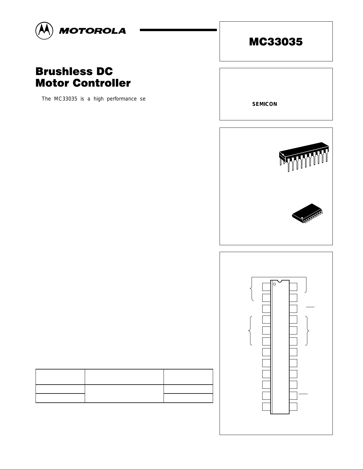
The MC33035 is a high performance second generation monolithic
brushless DC motor controller containing all of the active functions required
to implement a full featured open loop, three or four phase motor control
system. This device consists of a rotor position decoder for proper
commutation sequencing, temperature compensated reference capable of
supplying sensor power, frequency programmable sawtooth oscillator, three
open collector top drivers, and three high current totem pole bottom drivers
ideally suited for driving power MOSFETs.
Also included are protective features consisting of undervoltage lockout,
cycle–by–cycle current limiting with a selectable time delayed latched
shutdown mode, internal thermal shutdown, and a unique fault output that
can be interfaced into microprocessor controlled systems.
Typical motor control functions include open loop speed, forward or
reverse direction, run enable, and dynamic braking. The MC33035 is
designed to operate with electrical sensor phasings of 60°/300° or
120°/240°, and can also efficiently control brush DC motors.
• 10 to 30 V Operation
• Undervoltage Lockout
• 6.25 V Reference Capable of Supplying Sensor Power
• Fully Accessible Error Amplifier for Closed Loop Servo Applications
• High Current Drivers Can Control External 3–Phase MOSFET Bridge
• Cycle–By–Cycle Current Limiting
• Pinned–Out Current Sense Reference
• Internal Thermal Shutdown
• Selectable 60°/300° or 120°/240° Sensor Phasings
• Can Efficiently Control Brush DC Motors with External MOSFET
H–Bridge
ORDERING INFORMATION
Operating
Device
MC33035DW
MC33035P
Temperature Range
°
A
= –
o +
°
Package
SO–24L
Plastic DIP
Order this document by MC33035/D
BRUSHLESS DC
MOTOR CONTROLLER
SEMICONDUCTOR
TECHNICAL DATA
P SUFFIX
PLASTIC PACKAGE
CASE 724
DW SUFFIX
PLASTIC PACKAGE
CASE 751E
(SO–24L)
PIN CONNECTIONS
Top Drive
Output
Sensor
Inputs
Output Enable
Reference Output
Current Sense
Noninverting Input
Noninverting Input
Inverting Input
B
A
S
A
S
B
S
C
Oscillator
Error Amp
Error Amp
T
T
24
1
24
1
2
3
4
5
6
7
8
9
10
11
1
C
24
T
23
Brake
22
60°/120°SelectFwd/Rev
A
21
B
20
B
B
19
C
B
18
V
C
17
V
CC
Gnd
16
Current Sense
15
Inverting Input
14
Output
Fault
Error Amp Out/
1312
PWM Input
Bottom
Drive
Outputs
(Top View)
MOTOROLA ANALOG IC DEVICE DATA
Motorola, Inc. 1996 Rev 2
1
Fwd/Rev
60°/120
Enable
V
R
T
C
T
°
in
Speed
Set
Faster
17
18
11
12
13
10
4
5
6
3
2
7
8
Reference
Regulator
Error Amp
Oscillator
Undervoltage
Lockout
PWM
MC33035
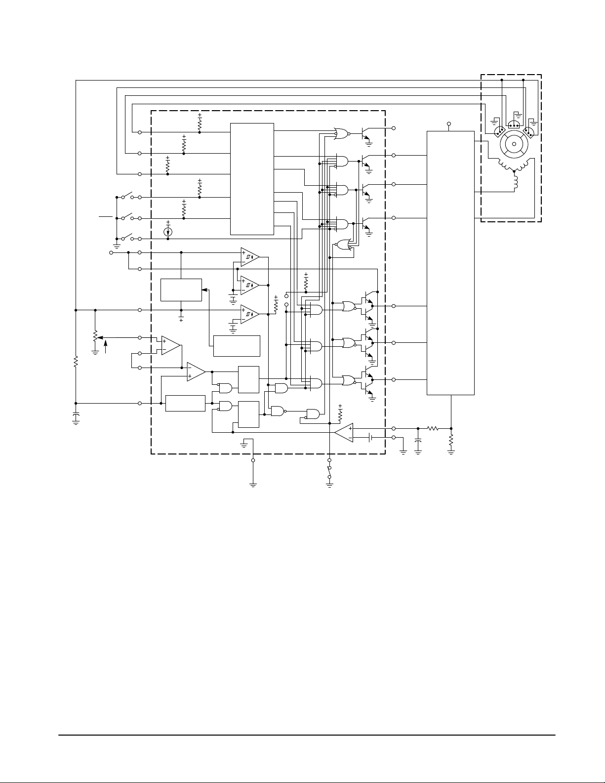
Representative Schematic Diagram
Rotor
Position
Decoder
Thermal
Shutdown
R
Q
S
S
Q
R
14
24
21
20
19
2
1
9
Fault
V
M
Output
Buffers
N
SS
N
Motor
2316
Brake
This device contains 285 active transistors.
15
Current Sense
Reference
2
MOTOROLA ANALOG IC DEVICE DATA
MC33035
MAXIMUM RATINGS
Rating Symbol Value Unit
Power Supply Voltage V
Digital Inputs (Pins 3, 4, 5, 6, 22, 23) – V
Oscillator Input Current (Source or Sink) I
Error Amp Input Voltage Range
(Pins 11, 12, Note 1)
Error Amp Output Current
(Source or Sink, Note 2)
Current Sense Input Voltage Range (Pins 9, 15) V
Fault Output Voltage V
Fault Output Sink Current I
Top Drive Voltage (Pins 1, 2, 24) V
Top Drive Sink Current (Pins 1, 2, 24) I
Bottom Drive Supply Voltage (Pin 18) V
Bottom Drive Output Current I
(Source or Sink, Pins 19, 20, 21)
Power Dissipation and Thermal Characteristics
P Suffix, Dual In Line, Case 724
Maximum Power Dissipation @ TA = 85°C P
Thermal Resistance, Junction–to–Air R
DW Suffix, Surface Mount, Case 751E
Maximum Power Dissipation @ TA = 85°C P
Thermal Resistance, Junction–to–Air R
Operating Junction Temperature T
Operating Ambient Temperature Range T
Storage Temperature Range T
CC
OSC
V
IR
I
Out
Sense
CE(Fault)
Sink(Fault)
CE(top)
Sink(top)
C
DRV
D
θ
JA
D
θ
JA
J
A
stg
–0.3 to V
–0.3 to 5.0 V
–40 to +85 °C
–65 to +150 °C
40 V
ref
V
30 mA
V
ref
10 mA
20 V
20 mA
40 V
50 mA
30 V
100 mA
867 mW
75 °C/W
650 mW
100 °C/W
150 °C
ELECTRICAL CHARACTERISTICS (V
Characteristic
= VC = 20 V, RT = 4.7 k, CT = 10 nF, TA = 25°C, unless otherwise noted.)
CC
Symbol Min Typ Max Unit
REFERENCE SECTION
Reference Output Voltage (I
T
= 25°C
A
T
= –40° to +85°C
A
Line Regulation (VCC = 10 to 30 V, I
Load Regulation (I
= 1.0 to 20 mA) Reg
ref
Output Short Circuit Current (Note 3) I
Reference Under Voltage Lockout Threshold V
= 1.0 mA)
ref
= 1.0 mA) Reg
ref
V
ref
line
load
SC
th
5.9
5.82
6.24
–
6.5
6.57
– 1.5 30 mV
– 16 30 mV
40 75 – mA
4.0 4.5 5.0 V
ERROR AMPLIFIER
Input Offset Voltage (T
Input Offset Current (T
Input Bias Current (T
Input Common Mode Voltage Range V
Open Loop Voltage Gain (VO = 3.0 V, RL = 15 k) A
= –40° to +85°C) V
A
= –40° to +85°C) I
A
= –40° to +85°C) I
A
IO
IO
IB
ICR
VOL
– 0.4 10 mV
– 8.0 500 nA
– –46 –1000 nA
(0 V to V
) V
ref
70 80 – dB
Input Common Mode Rejection Ratio CMRR 55 86 – dB
Power Supply Rejection Ratio (VCC = VC = 10 to 30 V) PSRR 65 105 – dB
NOTES: 1. The input common mode voltage or input signal voltage should not be allowed to go negative by more than 0.3 V.
2.The compliance voltage must not exceed the range of –0.3 to V
3.Maximum package power dissipation limits must be observed.
.
ref
V
MOTOROLA ANALOG IC DEVICE DATA
3

MC33035
Output Enable
µA
gp (IH)
IH
Bottom Drive Output Voltage
V
g(
CC C source
)
OH
(
CC
)
(
CC
)
Power Supply Current
mA
Pin 17 (VCC VC 20 V)
I
CC
121416
(
CC
0,C30 )
0
(
CC C
)
C
ELECTRICAL CHARACTERISTICS (continued) (V
Characteristic
= VC = 20 V, RT = 4.7 k, CT = 10 nF, TA = 25°C, unless otherwise noted.)
CC
Symbol Min Typ Max Unit
ERROR AMPLIFIER
Output Voltage Swing
High State (RL = 15 k to Gnd)
Low State (R
= 15 k to V
L
ref
)
V
OH
V
OL
4.6
–
0.5
5.3
–
1.0
OSCILLATOR SECTION
Oscillator Frequency f
Frequency Change with Voltage (VCC = 10 to 30 V) ∆f
Sawtooth Peak Voltage V
Sawtooth Valley Voltage V
OSC
/∆V – 0.01 5.0 %
OSC
OSC(P)
OSC(V)
22 25 28 kHz
– 4.1 4.5 V
1.2 1.5 – V
LOGIC INPUTS
Input Threshold Voltage (Pins 3, 4, 5, 6, 7, 22, 23)
High State
Low State
V
IH
V
IL
3.0
–
1.7
2.2
–
0.8
Sensor Inputs (Pins 4, 5, 6)
High State Input Current (VIH = 5.0 V)
Low State Input Current (V
= 0 V)
IL
I
IH
I
IL
–150
–600
–70
–337
–20
–150
Forward/Reverse, 60°/120° Select (Pins 3, 22, 23)
High State Input Current (V
Low State Input Current (V
= 5.0 V)
IH
= 0 V)
IL
I
IH
I
IL
–75
–300
–36
–175
–10
–75
Output Enable µA
High State Input Current (VIH = 5.0 V)
Low State Input Current (VIL = 0 V)
I
IH
I
IL
–60
–29
–10
–60 –29 –10
CURRENT–LIMIT COMPARATOR
Threshold Voltage V
Input Common Mode Voltage Range V
Input Bias Current I
th
ICR
IB
85 101 115 mV
– 3.0 – V
– –0.9 –5.0 µA
OUTPUTS AND POWER SECTIONS
Top Drive Output Sink Saturation (I
Top Drive Output Off–State Leakage (VCE = 30 V) I
= 25 mA) V
sink
CE(sat)
DRV(leak)
– 0.5 1.5 V
– 0.06 100 µA
Top Drive Output Switching Time (CL = 47 pF, RL = 1.0 k) ns
Rise Time t
Fall Time t
r
f
– 107 300
– 26 300
Bottom Drive Output Voltage V
High State (VCC = 20 V, VC = 30 V, I
Low State (VCC = 20 V, VC = 30 V, I
source
= 50 mA)
sink
= 50 mA)
V
OH
V
OL
(V
CC
–2.0) (V
–
–1.1)
CC
1.5 2.0
–
Bottom Drive Output Switching Time (CL = 1000 pF) ns
Rise Time t
Fall Time t
Fault Output Sink Saturation (I
= 16 mA) V
sink
Fault Output Off–State Leakage (VCE = 20 V) I
r
f
CE(sat)
FLT(leak)
– 38 200
– 30 200
– 225 500 mV
– 1.0 100 µA
Under Voltage Lockout V
Drive Output Enabled (VCC or V
Hysteresis V
Increasing) V
C
th(on)
H
8.2 8.9 10
0.1 0.2 0.3
Power Supply Current mA
Pin 17 (VCC = VC = 20 V) I
Pin 17 (VCC = 20 V, VC = 30 V)
Pin 18 (VCC = VC = 20 V) I
Pin 18 (VCC = 20 V, VC = 30 V)
CC
C
– 12 16
–
– 3.5
20
6.0
– 5.0 10
V
V
µA
µA
4
MOTOROLA ANALOG IC DEVICE DATA
MC33035
Figure 1. Oscillator Frequency versus
100
10
OSCILLA TOR FREQUENCY (kHz)
CT = 100 nF
,
OSC
f
0
1.0
Figure 3. Error Amp Open Loop Gain and
56
48
40
32
24
16
0
1.0 k
VCC = 20 V
= 20 V
V
C
= 3.0 V
V
O
= 15 k
R
L
= 100 pF
C
L
= 25°C
T
A
8.0
–8.0
, OPEN LOOP VOL TAGE GAIN (dB)
–16
VOL
A
–24
Timing Resistor
CT = 10 nF
, TIMING RESISTOR (kΩ)
R
T
CT = 1.0 nF
Phase versus Frequency
Phase
Gain
f, FREQUENCY (Hz)
VCC = 20 V
= 20 V
V
C
= 25°C
T
A
4.0
2.0
0
–2.0
OSCILLA T OR FREQUENCY CHANGE (%)
,
OSC
–4.0
f
100010010
40
∆
–55
0
60
80
– 0.8
100
120
–1.6
140
160
1.6
180
EXCESS PHASE (DEGREES)
,
200
φ
220
240
10 M1.0 M100 k10 k
, OUTPUT SA TURATION VOLTAGE (V)
V
sat
0.8
0
Figure 2. Oscillator Frequency Change
versus T emperature
VCC = 20 V
= 20 V
V
C
= 4.7 k
R
T
= 10 nF
C
T
TA, AMBIENT TEMPERATURE (°C)
Figure 4. Error Amp Output Saturation
V oltage versus Load Current
V
ref
Source Saturation
(Load to Ground)
Sink Saturation
Gnd
(Load to V
1.0 2.0
IO, OUTPUT LOAD CURRENT (mA)
)
ref
1007550250–25
VCC = 20 V
= 20 V
V
C
= 25°C
T
A
125
5.04.03.00
Figure 5. Error Amp Small–Signal
Transient Response
3.05
3.0
, OUTPUT VOL TAGE (V)
O
V
2.95
µ
s/DIV
1.0
MOTOROLA ANALOG IC DEVICE DATA
AV = +1.0
No Load
= 25°C
T
A
, OUTPUT VOL TAGE (V)
V
4.5
3.0
O
1.5
Figure 6. Error Amp Large–Signal
Transient Response
AV = +1.0
No Load
T
A
5.0 µs/DIV
= 25°C
5
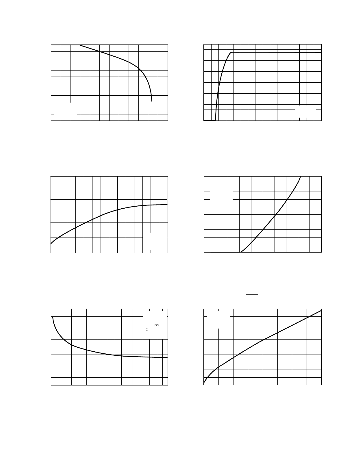
MC33035
Figure 7. Reference Output V oltage Change
versus Output Source Current
0
–4.0
–8.0
– 12
– 16
VCC = 20 V
–20
, REFERENCE OUTPUT VOLTAGE CHANGE (mV)
–24
ref
V
∆
= 20 V
V
C
= 25°C
T
A
0
, REFERENCE OUTPUT SOURCE CURRENT (mA)
I
ref
Figure 9. Reference Output Voltage
versus T emperature
40
20
0
–20
–40
, NORMALIZED REFERENCE VOLTAGE CHANGE (mV)
ref
V
∆
–25
–55 0
T
A
, AMBIENT TEMPERATURE (°C)
= 20 V
V
CC
= 20 V
V
C
No Load
Figure 8. Reference Output Voltage
versus Supply V oltage
7.0
6.0
5.0
4.0
3.0
2.0
1.0
, REFERENCE OUTPUT VOLTAGE (V)
ref
V
0
605040302010
0
V
, SUPPLY VOLT AGE (V)
CC
No Load
= 25°C
T
A
40302010
Figure 10. Output Duty Cycle versus
PWM Input Voltage
100
VCC = 20 V
= 20 V
V
C
= 4.7 k
R
80
60
40
20
OUTPUT DUTY CYCLE (%)
125100755025
T
= 10 nF
C
T
= 25°C
T
A
0
0
5.04.03.02.01.0
PWM INPUT VOLTAGE (V)
Figure 11. Bottom Drive Response T ime versus
Current Sense Input Voltage
250
200
150
100
50
, BOTTOM DRIVE RESPONSE TIME (ns)
HL
t
0
1.0 2.0 3.0 4.0 5.0 7.0 8.0 10
CURRENT SENSE INPUT VOLTAGE (NORMALIZED TO V
VCC = 20 V
V
R
CL = 1.0 nF
T
6.0 9.0
6
= 20 V
C
=
1
L
= 25°C
A
Figure 12. Fault
Output Saturation
versus Sink Current
0.25
VCC = 20 V
= 20 V
V
C
0.2
= 25°C
T
A
0.15
0.1
0.05
, OUTPUT SA TURATION VOLTAGE (V)V
sat
0
016128.04.0
)
th
, SINK CURRENT (mA)
I
Sink
MOTOROLA ANALOG IC DEVICE DATA
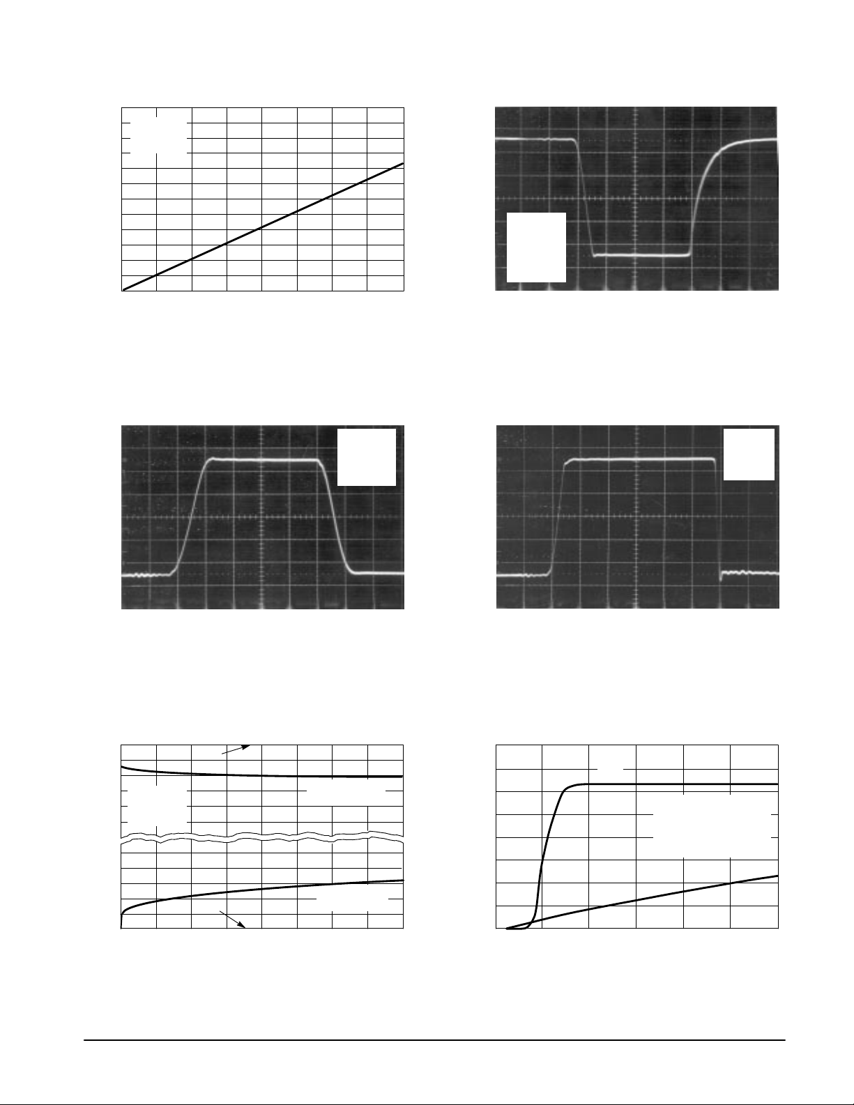
1.2
0.8
Figure 13. Top Drive Output Saturation
V oltage versus Sink Current
VCC = 20 V
= 20 V
V
C
= 25°C
T
A
MC33035
Figure 14. Top Drive Output Waveform
100
, OUTPUT SA TURATION VOLTAGE (V)
sat
V
OUTPUT VOLTAGE (%)
0
VCC = 20 V
= 20 V
V
C
= 1.0 k
R
L
= 15 pF
C
L
= 25°C
T
A
100 ns/DIV
0.4
0
0
10 30 40
I
Sink
20
, SINK CURRENT (mA)
Figure 15. Bottom Drive Output Waveform Figure 16. Bottom Drive Output Waveform
VCC = 20 V
= 20 V
V
100
C
= 1.0 nF
C
L
= 25°C
T
A
0
100
OUTPUT VOLTAGE (%) OUTPUT VOLTAGE (%)
0
VCC = 20 V
= 20 V
V
C
= 15 pF
C
L
= 25°C
T
A
, OUTPUT SA TURATION VOLTAGE (V)
V
50 ns/DIV
Figure 17. Bottom Drive Output Saturation
V oltage versus Load Current
–1.0
–2.0
2.0
1.0
sat
0
0
0
VCC = 20 V
= 20 V
V
C
= 25°C
T
A
V
C
Gnd
40
I
, OUTPUT LOAD CURRENT (mA)
O
Source Saturation
(Load to Ground)
Sink Saturation
(Load to V
)
C
50 ns/DIV
Figure 18. Power and Bottom Drive Supply
Current versus Supply Voltage
16
14
12
10
8.0
6.0
4.0
, POWER SUPPLY CURRENT (mA)
2.0
CC
, I
C
I
806020
0
0 5.0 10 15 20 25 30
I
CC
I
C
V
, SUPPLY VOLT AGE (V)
CC
RT = 4.7 k
= 10 nF
C
T
Pins 3–6, 9, 15, 23 = Gnd
Pins 7, 22 = Open
= 25°C
T
A
MOTOROLA ANALOG IC DEVICE DATA
7

MC33035
PIN FUNCTION DESCRIPTION
Pin Symbol Description
1, 2, 24 BT, AT, C
3 Fwd/Rev The Forward/Reverse Input is used to change the direction of motor rotation.
4, 5, 6 SA, SB, S
7 Output Enable A logic high at this input causes the motor to run, while a low causes it to coast.
8 Reference Output This output provides charging current for the oscillator timing capacitor CT and a
9 Current Sense Noninverting Input A 100 mV signal, with respect to Pin 15, at this input terminates output switch
10 Oscillator The Oscillator frequency is programmed by the values selected for the timing
11 Error Amp Noninverting Input This input is normally connected to the speed set potentiometer .
12 Error Amp Inverting Input This input is normally connected to the Error Amp Output in open loop applications.
13 Error Amp Out/PWM Input This pin is available for compensation in closed loop applications.
14 Fault Output This open collector output is active low during one or more of the following
15 Current Sense Inverting Input Reference pin for internal 100 mV threshold. This pin is normally connected to the
16 Gnd This pin supplies a ground for the control circuit and should be referenced back to
17 V
18 V
19, 20, 21 CB, BB, A
22 60°/120° Select The electrical state of this pin configures the control circuit operation for either 60°
23 Brake A logic low state at this input allows the motor to run, while a high state does not
T
C
CC
C
B
These three open collector Top Drive outputs are designed to drive the external
upper power switch transistors.
These three Sensor Inputs control the commutation sequence.
reference for the error amplifier. It may also serve to furnish sensor power.
conduction during a given oscillator cycle. This pin normally connects to the top
side of the current sense resistor.
components, R
conditions: Invalid Sensor Input code, Enable Input at logic 0, Current Sense Input
greater than 100 mV (Pin 9 with respect to Pin 15), Undervoltage Lockout
activation, and Thermal Shutdown.
bottom side of the current sense resistor.
the power source ground.
This pin is the positive supply of the control IC. The controller is functional over a
minimum V
The high state (VOH) of the Bottom Drive Outputs is set by the voltage applied to
this pin. The controller is operational over a minimum V
These three totem pole Bottom Drive Outputs are designed for direct drive of the
external bottom power switch transistors.
(high state) or 120° (low state) sensor electrical phasing inputs.
allow motor operation and if operating causes rapid deceleration.
and CT.
T
range of 10 to 30 V.
CC
range of 10 to 30 V.
C
INTRODUCTION
The MC33035 is one of a series of high performance
monolithic DC brushless motor controllers produced by
Motorola. It contains all of the functions required to
implement a full–featured, open loop, three or four phase
motor control system. In addition, the controller can be made
to operate DC brush motors. Constructed with Bipolar Analog
technology, it offers a high degree of performance and
ruggedness in hostile industrial environments. The MC33035
contains a rotor position decoder for proper commutation
sequencing, a temperature compensated reference capable
of supplying a sensor power, a frequency programmable
sawtooth oscillator, a fully accessible error amplifier, a pulse
width modulator comparator, three open collector top drive
outputs, and three high current totem pole bottom driver
outputs ideally suited for driving power MOSFETs.
Included in the MC33035 are protective features
consisting of undervoltage lockout, cycle–by–cycle current
limiting with a selectable time delayed latched shutdown
mode, internal thermal shutdown, and a unique fault output
that can easily be interfaced to a microprocessor controller.
Typical motor control functions include open loop speed
control, forward or reverse rotation, run enable, and dynamic
braking. In addition, the MC33035 has a 60°/120
which configures the rotor position decoder for either 60° or
120° sensor electrical phasing inputs.
° select pin
FUNCTIONAL DESCRIPTION
A representative internal block diagram is shown in
Figure 19 with various applications shown in Figures 36, 38,
39, 43, 45, and 46. A discussion of the features and function
of each of the internal blocks given below is referenced to
Figures 19 and 36.
Rotor Position Decoder
An internal rotor position decoder monitors the three
sensor inputs (Pins 4, 5, 6) to provide the proper sequencing
of the top and bottom drive outputs. The sensor inputs are
designed to interface directly with open collector type Hall
Effect switches or opto slotted couplers. Internal pull–up
resistors are included to minimize the required number of
external components. The inputs are TTL compatible, with
their thresholds typically at 2.2 V. The MC33035 series is
designed to control three phase motors and operate with four
of the most common conventions of sensor phasing. A
60°/120
the MC33035 to configure itself to control motors having
either 60°, 120°, 240° or 300° electrical sensor phasing. With
three sensor inputs there are eight possible input code
combinations, six of which are valid rotor positions. The
remaining two codes are invalid and are usually caused by an
open or shorted sensor line. With six valid input codes, the
° Select (Pin 22) is conveniently provided and affords
8
MOTOROLA ANALOG IC DEVICE DATA
 Loading...