

Motorola MC33033DWR2, MC33033P, MC33033DW Datasheet
T
40° t
85°C
The MC33033 is a high performance second generation, limited feature,
monolithic brushless dc motor controller which has evolved from Motorola′s
full featured MC33034 and MC33035 controllers. It contains all of the active
functions required for the implementation of open loop, three or four phase
motor control. The device consists of a rotor position decoder for proper
commutation sequencing, temperature compensated reference capable of
supplying sensor power, frequency programmable sawtooth oscillator, fully
accessible error amplifier, pulse width modulator comparator, three open
collector top drivers, and three high current totem pole bottom drivers ideally
suited for driving power MOSFETs. Unlike its predessors, it does not feature
separate drive circuit supply and ground pins, brake input, or fault output
signal.
Included in the MC33033 are protective features consisting of
undervoltage lockout, cycle–by–cycle current limiting with a selectable time
delayed latched shutdown mode, and internal thermal shutdown.
Typical motor control functions include open loop speed, forward or
reverse direction, and run enable.The MC33033 is designed to operate
brushless motors with electrical sensor phasings of 60°/300° or 120°/240°,
and can also efficiently control brush dc motors.
Order this document by MC33033/D
BRUSHLESS DC
MOTOR CONTROLLER
SEMICONDUCTOR
TECHNICAL DATA
20
1
P SUFFIX
PLASTIC PACKAGE
CASE 738
• 10 to 30 V Operation
• Undervoltage Lockout
• 6.25 V Reference Capable of Supplying Sensor Power
• Fully Accessible Error Amplifier for Closed Loop Servo Applications
• High Current Drivers Can Control External 3–Phase MOSFET Bridge
• Cycle–By–Cycle Current Limiting
• Internal Thermal Shutdown
• Selectable 60°/300° or 120°/240° Sensor Phasings
• Also Efficiently Control Brush DC Motors with External MOSFET
H–Bridge
ORDERING INFORMATION
Operating
Device
MC33033DW
MC33033P
Temperature Range
°
A
= –
o +
°
Package
SO–20L
Plastic DIP
20
PLASTIC PACKAGE
PIN CONNECTIONS
Top Drive
Output
Sensor
Inputs
Reference Output
Non Inverting Input
Inverting Input
B
T
A
T
S
A
S
B
S
C
Oscillator
Error Amp
Error Amp
1
DW SUFFIX
CASE 751D
(SO–20L)
1
2
3
4
5
6
7
8
9
10
20
C
T
19
Output Enable
18
°
/120°SelectFwd/Rev
60
A
17
B
16
15
14
13
12
11
Bottom
B
Drive
B
Outputs
C
B
V
CC
Gnd
Current Sense
Non Inverting Input
Error Amp Out/
PWM Input
(Top View)
Motorola, Inc. 1996 Rev 3
MOTOROLA ANALOG IC DEVICE DATA
1
FWR/REV
60°/120
Enable
Speed
Set
R
T
C
T
°
V
Faster
CC
Reference
Regulator
Error Amp
Oscillator
PWM
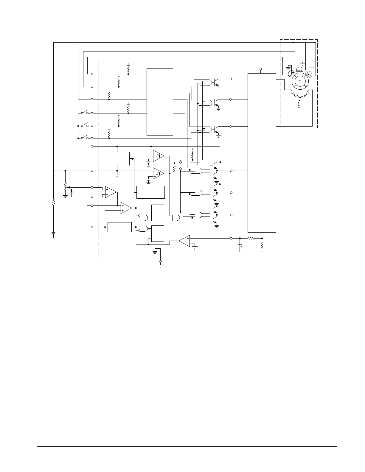
MC33033
Representative Schematic Diagram
Rotor
Position
Decoder
Undervoltage
Lockout
Thermal
Shutdown
R
Q
S
S
Q
R
V
M
Output
Buffers
N
SS
N
Motor
This device contains 266 active transistors.
Current Sense
2
MOTOROLA ANALOG IC DEVICE DATA
MC33033
MAXIMUM RATINGS
Rating Symbol Value Unit
Power Supply Voltage V
Digital Inputs (Pins 3, 4, 5, 6, 18, 19) – V
Oscillator Input Current (Source or Sink) I
Error Amp Input Voltage Range
(Pins 9, 10, Note 1)
Error Amp Output Current
(Source or Sink, Note 2)
Current Sense Input Voltage Range V
Top Drive V oltage (Pins 1, 2, 20) V
Top Drive Sink Current (Pins 1, 2, 20) I
Bottom Drive Output Current
(Source or Sink, Pins 15,16, 17)
Power Dissipation and Thermal Characteristics
P Suffix, Dual–In–Line, Case 738
Maximum Power Dissipation @ TA = 85°C P
Thermal Resistance, Junction–to–Air R
DW Suffix, Surface Mount, Case 751D
Maximum Power Dissipation @ TA = 85°C P
Thermal Resistance, Junction–to–Air R
Operating Junction Temperature T
Operating Ambient Temperature Range T
Storage Temperature Range T
CC
OSC
V
IR
I
Out
Sense
CE(top)
Sink(top)
I
DRV
D
θJA
D
θJA
J
A
stg
–0.3 to V
–0.3 to 5.0 V
–40 to +85 °C
–65 to +150 °C
30 V
ref
30 mA
ref
10 mA
40 V
50 mA
100 mA
867 mW
75 °C/W
619 mW
105 °C/W
150 °C
V
V
ELECTRICAL CHARACTERISTICS (V
Characteristic
REFERENCE SECTION
Reference Output Voltage (I
TA = 25°C
TA = –40° to + 85°C
Line Regulation (VCC = 10 V to 30 V, I
Load Regulation (I
Output Short–Circuit Current (Note 3) I
Reference Under Voltage Lockout Threshold V
ERROR AMPLIFIER
Input Offset Voltage (TA = –40° to + 85°C) V
Input Offset Current (TA = –40° to + 85°C) I
Input Bias Current (TA = –40° to + 85°C) I
Input Common Mode Voltage Range V
Open Loop Voltage Gain (VO = 3.0 V, RL = 15 k) A
Input Common Mode Rejection Ratio CMRR 55 86 – dB
Power Supply Rejection Ratio (VCC = 10 V to 30 V) PSRR 65 105 – dB
Output Voltage Swing
High State (RL = 15 k to Gnd)
Low State (RL = 17 k to V
NOTES: 1. The input common mode voltage or input signal voltage should not be allowed to go negative by more than 0.3 V.
2.The compliance voltage must not exceed the range of –0.3 to V
3.Maximum package power dissipation limits must be observed.
= 1.0 mA to 20 mA) Reg
ref
= 1.0 mA)
ref
)
ref
= 20 V, RT = 4.7 k, CT = 10 nF, TA = 25°C, unless otherwise noted.)
CC
Symbol Min Typ Max Unit
V
= 1.0 mA) Reg
ref
ref
ref
line
load
SC
th
IO
IO
IB
ICR
VOL
V
OH
V
OL
.
5.9
5.82
– 1.5 30 mV
– 16 30 mV
40 75 – mA
4.0 4.5 5.0 V
– 0.4 10 mV
– 8.0 500 nA
– –46 –1000 nA
70 80 – dB
4.6
–
6.24
–
(0 V to V
5.3
0.5
6.5
6.57
ref)
–
1.0
V
V
V
MOTOROLA ANALOG IC DEVICE DATA
3

MC33033
ELECTRICAL CHARACTERISTICS
Characteristic
OSCILLATOR SECTION
Oscillator Frequency f
Frequency Change with Voltage (VCC = 10 V to 30 V) ∆f
Sawtooth Peak Voltage V
Sawtooth Valley Voltage V
LOGIC INPUTS
Input Threshold Voltage (Pins 3, 4, 5, 6, 18, 19)
High State
Low State
Sensor Inputs (Pins 4, 5, 6)
High State Input Current (VIH = 5.0 V)
Low State Input Current (VIL = 0 V)
Forward/Reverse, 60°/120° Select and Output Enable
(Pins 3, 18, 19)
High State Input Current (VIH = 5.0 V)
Low State Input Current (VIL = 0 V)
CURRENT–LIMIT COMPARATOR
Threshold Voltage V
Input Common Mode Voltage Range V
Input Bias Current I
OUTPUTS AND POWER SECTIONS
Top Drive Output Sink Saturation (I
Top Drive Output Off–State Leakage (VCE = 30 V) I
Top Drive Output Switching Time (CL = 47 pF, RL = 1.0 k)
Rise Time
Fall Time
Bottom Drive Output Voltage
High State (VCC = 30 V, I
Low State (VCC = 30 V, I
Bottom Drive Output Switching Time (CL = 1000 pF)
Rise Time
Fall Time
Under Voltage Lockout
Drive Output Enabled (VCC Increasing)
Hysteresis
Power Supply Current I
source
sink
= 50 mA)
(continued) (VCC = 20 V, RT = 4.7 k, CT = 10 nF, TA = 25°C, unless otherwise noted.)
= 25 mA) V
Sink
DRV(leak)
= 50 mA)
Symbol Min Typ Max Unit
OSC
/∆V – 0.01 5.0 %
OSC
OSC(P)
OSC(V)
V
IH
V
IL
I
IH
I
IL
I
IH
I
IL
th
ICR
IB
CE(sat)
t
r
t
f
V
OH
V
OL
t
r
t
f
V
th(on)
V
H
CC
22 25 28 kHz
– 4.1 4.5 V
1.2 1.5 – V
3.0
–
–150
–600
–75
–300
85 101 115 mV
– 3.0 – V
– –0.9 –5.0 µA
– 0.5 1.5 V
– 0.06 100 µA
–
–
(VCC – 2.0)–(VCC – 1.1)
–
–
8.2
0.1
– 15 22 mA
2.2
1.7
–70
–337
–36
–175
107
26
1.5
38
30
8.9
0.2
–
0.8
–20
–150
–10
–75
300
300
–
2.0
200
200
10
0.3
V
µA
µA
ns
V
ns
V
4
MOTOROLA ANALOG IC DEVICE DATA
MC33033
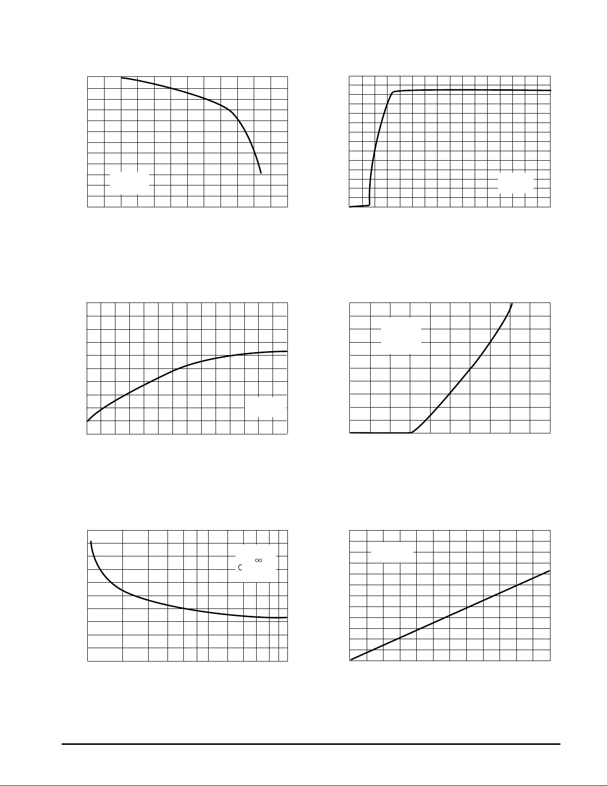
Figure 1. Oscillator Frequency versus
100
10
OSCILLA TOR FREQUENCY (kHz)
CT = 100 nF
,
OSC
f
0
1.0
Figure 3. Error Amp Open Loop Gain and
56
48
40
32
24
16
VCC = 20 V
8.0
VO = 3.0 V
RL = 15 k
0
CL = 100 pF
–8.0
, OPEN–LOOP VOLTAGE GAIN (dB)
TA = 25
–16
VOL
A
–24
1.0 k
Timing Resistor
CT = 10 nF
RT, TIMING RESISTOR (kΩ)
Phase versus Frequency
Gain
°
C
f, FREQUENCY (Hz)
VCC = 20 V
TA = 25
CT = 1.0 nF
Phase
Figure 2. Oscillator Frequency Change
versus T emperature
4.0
°
C
100010010
2.0
0
–2.0
OSCILLA T OR FREQUENCY CHANGE (%)
,
OSC
–4.0
f
∆
–55
VCC = 20 V
RT = 4.7 k
CT = 10 nF
TA, AMBIENT TEMPERATURE (°C)
125
1007550250–25
Figure 4. Error Amp Output Saturation
V oltage versus Load Current
40
60
80
100
120
140
160
180
EXCESS PHASE (DEGREES)
,
200
φ
220
240
10M1.0 M100 k10 k
– 0.8
–1.6
, OUTPUT SA TURATION VOLTAGE (V)
sat
V
1.6
0.8
0
0
V
ref
Source Saturation
(Load to Ground)
Sink Saturation
Gnd
1.0 2.0
IO, OUTPUT LOAD CURRENT (mA)
(Load to V
ref
VCC = 20 V
TA = 25
)
°
C
5.04.03.00
Figure 5. Error Amp Small–Signal
Transient Response
3.05
3.0
, OUTPUT VOL TAGE (V)
O
V
2.95
µ
s/DIV
1.0
MOTOROLA ANALOG IC DEVICE DATA
AV = +1.0
No Load
°
TA = 25
Figure 6. Error Amp Large–Signal
Transient Response
AV = +1.0
No Load
TA = 25
°
C
, OUTPUT VOL TAGE (V)
V
O
4.5
3.0
1.5
5.0 µs/DIV
C
5
MC33033
Figure 7. Reference Output V oltage Change
versus Output Source Current
0
–4.0
–8.0
– 12
– 16
0
VCC = 20 V
°
C
TA = 25
I
, REFERENCE OUTPUT SOURCE CURRENT (mA)
ref
–20
REFERENCE OUTPUT VOL TAGE CHANGE (mV)
–24
ref,
V
∆
Figure 9. Reference Output Voltage
versus T emperature
40
20
0
–20
–40
NORMALIZED REFERENCE VOLTAGE CHANGE (mV)
ref,
V
∆
–25
–55 0
TA, AMBIENT TEMPERATURE (
°
C)
VCC = 20 V
No Load
Figure 8. Reference Output V oltage versus
Supply V oltage
7.0
6.0
5.0
4.0
3.0
2.0
REFERENCE OUTPUT VOLTAGE (V)
1.0
ref,
V
0
605040302010
0
VCC, SUPPLY VOLTAGE (V)
No Load
TA = 25
°
C
40302010
Figure 10. Output Duty Cycle versus
PWM Input Voltage
100
80
60
40
20
OUTPUT DUTY CYCLE (%)
125100755025
0
0
VCC = 20 V
RT = 4.7 k
CT = 10 nF
°
C
TA = 25
PWM INPUT VOLTAGE (V)
5.04.03.02.01.0
Figure 11. Bottom Drive Response T ime versus
Current Sense Input Voltage
250
200
150
100
50
, BOTTOM DRIVE RESPONSE TIME (ns)
HL
t
0
1.0 2.0 3.0 4.0 5.0 7.0 8.0 10
V
, CURRENT SENSE INPUT VOLTAGE (NORMALIZED TO Vth)
Sense
VCC = 20 V
RL =
CL = 1.0 nF
TA = 25
6.0 9.0
6
Figure 12. Top Drive Output Saturation Voltage
versus Sink Current
1.2
VCC = 20 V
°
C
1
, OUTPUT SA TURATION VOLTAGE (V)V
sat
0.8
0.4
0
°
C
TA = 25
040302010
I
, SINK CURRENT (mA)
Sink
MOTOROLA ANALOG IC DEVICE DATA
MC33033
OUTPUT VOLTAGE (%)
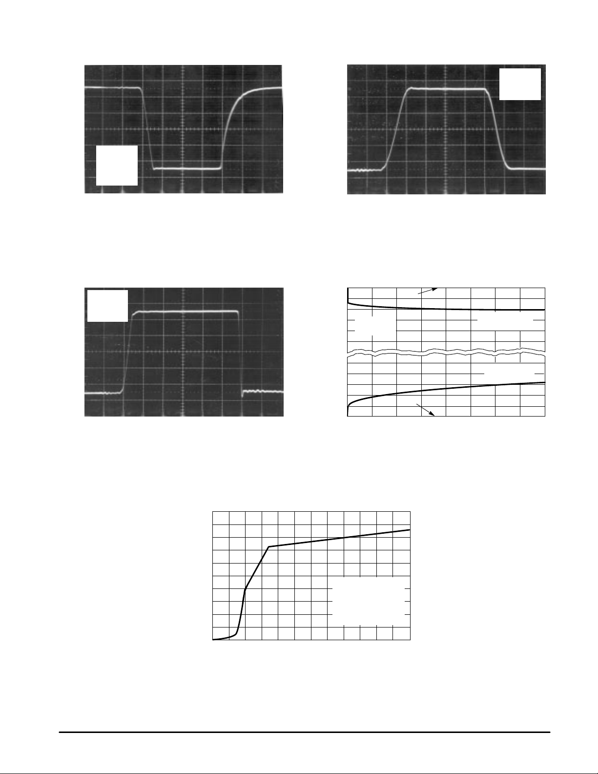
Figure 13. Top Drive Output Waveform
100
VCC = 20 V
RL = 1.0 k
0
CL = 15 pF
°
C
TA = 25
50 ns/DIV
Figure 15. Bottom Drive Output Waveform
VCC = 20 V
CL = 15 pF
°
C
TA = 25
100
OUTPUT VOLTAGE (%)
Figure 14. Bottom Drive Output Waveform
100
0
50 ns/DIV
Figure 16. Bottom Drive Output Saturation
V oltage versus Load Current
–1.0
–2.0
0
VCC = 20 V
TA = 25
V
CC
°
C
VCC = 20 V
CL = 1.0 nF
°
C
TA = 25
Source Saturation
(Load to Ground)
OUTPUT VOLTAGE (%)
2.0
0
50 ns/DIV
, OUTPUT SA TURATION VOLTAGE (V)
V
sat
1.0
Gnd
0
0
IO, OUTPUT LOAD CURRENT (mA)
40
Sink Saturation
(Load to VCC)
806020
Figure 17. Supply Current versus V oltage
20
18
16
14
12
8.0
6.0
4.0
, POWER SUPPLY CURRENT (mA)
CC
2.0
I
10
0
0
VCC, SUPPLY VOLTAGE (V)
RT = 4.7 k
CT = 10 nF
Pins 3–6, 12, 13 = Gnd
Pins 18, 19 = Open
°
C
TA = 25
30252015105.0
MOTOROLA ANALOG IC DEVICE DATA
7

MC33033
PIN FUNCTION DESCRIPTION
Pin Symbol Description
1, 2, 20 BT, AT, C
3 Fwd//Rev The Forward/Reverse Input is used to change the direction of motor rotation.
4, 5, 6 SA, SB, S
7 Reference Output This output provides charging current for the oscillator timing capacitor CT and a
8 Oscillator The Oscillator frequency is programmed by the values selected for the timing
9 Error Amp Noninverting Input This input is normally connected to the speed set potentiometer.
10 Error Amp Inverting Input This input is normally connected to the Error Amp Output in open loop applications.
11 Error Amp Out/PWM Input This pin is available for compensation in closed loop applications.
12 Current Sense Noninverting Input A 100 mV signal, with respect to Pin 13, at this input terminates output switch conduction
13 Gnd This pin supplies a separate ground return for the control circuit and should be
14 V
15, 16, 17 CB, BB, A
18 60°/120° Select The electrical state of this pin configures the control circuit operation for either 60°
19 Output Enable A logic high at this input causes the motor to run, while a low causes it to coast.
T
C
CC
B
These three open collector Top Drive Outputs are designed to drive the external upper
power switch transistors.
These three Sensor Inputs control the commutation sequence.
reference for the Error Amplifier . It may also serve to furnish sensor power.
components, RT and CT.
during a given oscillator cycle. This pin normally connects to the top side of the current
sense resistor.
referenced back to the power source ground.
This pin is the positive supply of the control IC. The controller is functional over a V
range of 10 to 30 V .
These three totem pole Bottom Drive Outputs are designed for direct drive of the external
bottom power switch transistors.
(high state) or 120° (low state) sensor electrical phasing inputs.
CC
8
MOTOROLA ANALOG IC DEVICE DATA
 Loading...